 Open Access Article
Helical SiNW design with a dual-peak response for broadband scattering in translucent solar cells†
Zhongliang
Gao
 a,
Qi
Geng
b,
Zhe
Wang
a,
Ting
Gao
b,
Yingfeng
Li
a,
Qi
Geng
b,
Zhe
Wang
a,
Ting
Gao
b,
Yingfeng
Li
 a,
Lei
Chen
b and
Meicheng
Li
 *a
*a
aState Key Laboratory of Alternate Electrical Power System with Renewable Energy Sources, School of New Energy, North China Electric Power University, Beijing, 102206, China
bSchool of Mathematics and Physics, North China Electric Power University, Beijing, 102206, China. E-mail: mcli@ncepu.edu.cn
First published on 13th December 2021
Abstract
Nanowires are widely used in optics, optoelectronics, photocatalysis, and photovoltaics because of their special optical properties. However, the narrow response spectrum of silicon nanowires (SiNWs) reduces the advantages of applications in photovoltaics. In this work, we designed a helical SiNW with an adjustable ultra-wide scattering spectrum for improving the light absorption of translucent solar cells by a simulation method combining optical and electrical dual physical fields. It is found that the helical SiNWs have three independent controllable characteristic scales to produce a dual-peak response in the scattering spectrum. Moreover, the position of the first peak can be accurately adjusted according to the comprehensive equation, and the radius and radial distance of the helix can adjust the position of the second peak. In addition, the distance between the two peaks can be flexibly adjusted to achieve a wide response spectrum, which realizes basically coverage of the optical gap absorption range of Si materials. Finally, the helical SiNWs are applied to a translucent SiNW array solar cell, and the light absorption increased to 40.86%, and the power conversion efficiency (PCE) increased to 5.85%, which is 40.03% and 50.39% higher than that of the cylindrical SiNW array solar cell, respectively.
1. Introduction
Nanowires have excellent optical and electrical properties to be widely used in photovoltaics, photoelectric, sensors, biology, and other fields.1–7 Silicon nanowire (SiNW) is a typical semiconductor nanowire, which combines the semiconductor properties of Si materials and nano-scale optical effects.8–10 It is applied in photoelectric conversion and energy storage devices.11,12 A single SiNW has excellent optical focusing performance, and it can achieve light absorption several times its own area and scattering dozens of times its own area.13–16 The light scattering and absorption generated by a single SiNW are coupled in the SiNW array to achieve a good light trapping effect on the Si surface.10,17,18 The new generation of Si-based solar cells prepared using SiNWs as the active layer is expected to break through the limitations of traditional solar cells, such as no toughness, no light transmission, bulky volume, and so on.19,20 However, the light absorption of this translucent solar cell without Si substrate depends more on the optical properties of a single SiNW.The peak in the response spectra of a single SiNW is usually only one, with strong intensity and narrow width.14–16,21 The intensity of the peak depends on the height of the SiNW, and the position of the peak can be adjusted by the diameter of the SiNW, but the width of the peak is difficult to adjust. According to the phenomenon that different scales of a single SiNW correspond to different peaks, researchers designed SiNWs with multiple scales, such as trilobal SiNWs, conical SiNWs, funnel-shaped SiNWs, etc.22–25 In our previous research study, we proposed a comprehensive equation of SiNWs according to these laws to quantitatively establish the relationship between the scale and the peak of SiNWs.26 In addition, according to the leaky mode theory of waveguide, the shape of SiNWs is designed for more modes, and the response spectrum width of SiNW is improved by more peaks.27,28 However, the range difference of different scales is small, the position of the peak is close, and the expansion of the peak width is very limited. Moreover, there is a strong correlation between the positions of the peaks in the SiNWs that broaden the spectrum by increasing the number of peaks. Therefore, it is difficult to realize the independent regulation of multiple peaks, which reduces the ability of response spectrum regulation.
In this work, a helical SiNW with a three-dimensional scale was designed, which has two peaks in the response spectrum, and each peak can be adjusted independently. The cylindrical radius can accurately adjust the position of the first peak, and the helical radius and radial distance can adjust the position of the second peak. The distance of the two peaks can be adjusted in the range of 200 to 900 nm, more importantly, the width of the two peaks almost covers the optical band gap absorption range of the Si material. When helical SiNWs are applied to translucent SiNW array solar cells, it increases the width of the light absorption spectrum, especially at the wavelength of 400 nm. Finally, the light absorption of translucent solar cells with helical SiNW array is increased by 40.02% and the power conversion efficiency (PCE) is increased by 50.39%.
2. Methods
All optical calculations are performed by the finite element method (FEM) and all electrical calculations by the finite volume method (FVM) through the software COMSOL Multiphysics 5.6a. The refractive index of all materials is derived from the online database refractiveindex.inf. The three-dimensional models of SiNWs, SiNW arrays, and electrical models of SiNW arrays are built in the software with their own CAD tools. Different SiNWs have the same volume or the same height. The geometric parameters of each SiNW used in the calculation are listed in the ESI† in detail. All calculations have been verified in the previous work to ensure the accuracy of the calculation.20,29The model of light scattering, absorption, and extinction of a single SiNW is set as the cube space as the calculation domain, and a perfect matching layer (PML) with a thickness greater than half a wavelength is set outside the calculation domain to simulate the absorption of scattered light. The detailed geometric parameters of the model are in the ESI.† The maximum value of the finite element mesh is set to be less than one-sixth of the wavelength in the medium to ensure the accuracy of the calculation. The reflectivity, absorptivity, and transmissivity of SiNW arrays are set as the calculation domain with periodic boundary conditions, and the perfect matching layers with a thickness greater than half the wavelength are set at the upper and lower ends to simulate the light absorption at infinity. The detailed geometric parameters of the model are in the ESI.† The maximum value of the finite element mesh is set to be less than one-sixth of the wavelength in the medium to ensure the accuracy of the calculation. The electrical model of the nanowire array solar cell is a three-dimensional model, which is calculated by FVM. The optical absorption used in the electrical calculation is the optical absorption obtained in the SiNW array. The two ends of the model are set as metal contact, PEDOT:PSS is the heterojunction contact with Si, the impurity concentration of Si material is 1016 cm−3, and the scanning voltage range is 0 to 0.7 V.
3. Design and optical properties of helical SiNWs
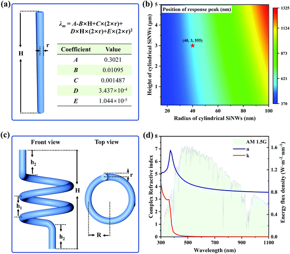
According to the research experience of SiNWs, we proposed a comprehensive equation in our previous research, which can effectively predict the relationship between the response peak of SiNWs and geometric parameters, as shown in Fig. 1a.26 The comprehensive equation is as follows,| λ = A – B × H + C × (2 × r) + D × H × (2 × r) + E × (2 × r)2 | (1) |
Through the comprehensive equation of cylindrical SiNWs, we designed helical SiNWs, and the structural diagram is shown in Fig. 1c. The radius r of the cylindrical SiNW is the first scale, the helical radius R is the second scale, and the helical radial distance h1 is the third scale. The scale of the cylinder is quite different from that of the helix, and the corresponding peaks should be far away. Compared with the previously designed SiNWs, it has a wider response spectrum. In the comprehensive equation, it can be concluded that the different heights of cylindrical SiNWs have a negligible effect on the position of the peak, so the position of h1 first peak has little effect. When the volume, cylindrical radius, and helical radius remain unchanged, the radial distance h2 increases, which will make the helical SiNWs closer to the cylindrical SiNWs. The second peak weakens and gradually disappears with the increase in radial distance h2. The refractive index of the Si material and AM1.5G spectral data are shown in Fig. 1d. When the wavelength is greater than 500 nm, the imaginary part in the complex refractive index of the Si material is very small, which indicates that the light absorption of Si becomes very weak. At this time, the corresponding light intensity is at the maximum position. Therefore, in order to improve the light absorption of Si in this wavelength range, we selected a radius of 40 nm and a height of 3 μm cylindrical SiNWs as a control, and then helical SiNWs were designed. The cylindrical radius of helical SiNWs is set to 40 nm, and the position of the corresponding first peak should also correspond to about 500 nm. The position regulation of the first peak is relatively clear, and the position of the second peak should be the focus of the exploration of the helical SiNWs.
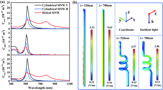
The scattering, absorption, and extinction spectra of cylindrical and helical SiNWs are calculated by FEM, as shown in Fig. 2a. The relationship between the three can be expressed by the following formula,
| Cext = Cabs + Csca | (2) |
In contrast, cylindrical SiNWs have only one peak in the scattering, absorption, and extinction spectra, as shown in Fig. 2a. The volume of cylindrical SiNW V is the same as that of helical SiNW, and the height of cylindrical SiNW H is the same as that of helical SiNW. Fig. 2b is the electric field distribution diagram of cylindrical SiNW V. When the incident light wavelength is 520 nm, the electric field intensity of cylindrical SiNWs is large, and the maximum electric field intensity is 5.23 V m−1, which is 0.66 V m−1 higher than the maximum electric field intensity of helical SiNWs of 4.57 V m−1. When the wavelength of incident light is 780 nm, the maximum electric field intensity of cylindrical SiNWs is 0.63 V m−1, which is much lower than that of helical SiNWs. It is proved that the helical SiNWs have two peaks due to two different structures. In helical SiNWs, the position of the first peak can be adjusted by the cylindrical radius, which is basically consistent with the variation law of cylindrical SiNWs and conforms to the law expressed by the comprehensive equation of cylindrical SiNWs. The position of the second peak is determined by the helix. The relationship between the two characteristic scales of the helix, radial distance and helix radius, and the position of the second peak is uncertain.
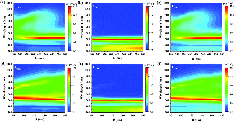
The relationship between the helical radial distance and helical radius of helical SiNWs and the response spectrum is explored, and the results are shown in Fig. 3. The response spectrum corresponding to the helical radial distance ranging from 160 to 800 nm is shown in Fig. 3a–c. With the increase in radial distance, the position of the second peak undergoes a redshift. When the radial distance increases to 400 nm, the intensity of the second peak increases to the maximum and gradually weakens and disappears. The position of the first peak hardly changes, but the intensity increases with the increase in radial distance. This is because on the premise of keeping the volume unchanged, with the increase in radial distance, the number of helical rings gradually decreases and becomes closer to the shape of cylindrical SiNWs. When the radial distance increases to 800 nm, it is consistent with the response spectral characteristics of cylindrical SiNWs. The response spectrum corresponding to the helical radius range of 80 to 180 nm is shown in Fig. 3d–f.
With the increase in helical radius, the position of the second response peak gradually redshifts. Compared with the regulation of radial distance, the adjustable range of the position of the second peak is larger. Therefore, the position of the second peak can be adjusted by a combination of helical radial distance and radius. The position of the first peak will also blue shift with the increase in helical radius, but the moving range is small. It can be considered that the geometric parameters of the helix have little effect on the position of the first peak.
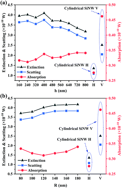
The purpose of broadening the response spectrum range of SiNWs is to obtain more light absorption as much as possible in photovoltaic applications. Combined with the solar spectrum AM1.5G, the total energy of extinction, scattering, and absorption of SiNWs under different geometric parameters are calculated by the following formula,
 | (3) |
With the increase in helical radius, the extinction and scattering energy increase gradually. This is because the width of the response spectrum increase of the helical radius, and the scattering and extinction energy increases with the increase of the response spectrum width. Light absorption showed a downward trend first and then an upward trend. It can be found from Fig. 3e that with the increase in the radius of the helix, the position of the peak of the absorption spectrum basically does not change, but the light absorption intensity in the wavelength range of 300 to 400 nm gradually increases, which makes the total light absorption also show an increasing trend. In contrast, the light absorption of a single cylindrical SiNW is much greater than that of helical SiNWs, and the scattering and extinction ability is much lower than that of helical SiNWs. In SiNW array solar cells, due to the limitation of light absorption of Si materials, scattered light energy is more important for long-band light absorption.
4. Optical and electrical properties of helical SiNW array solar cells
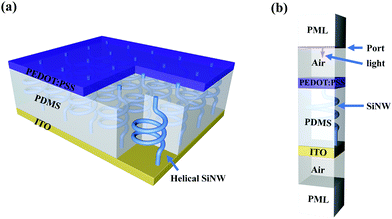
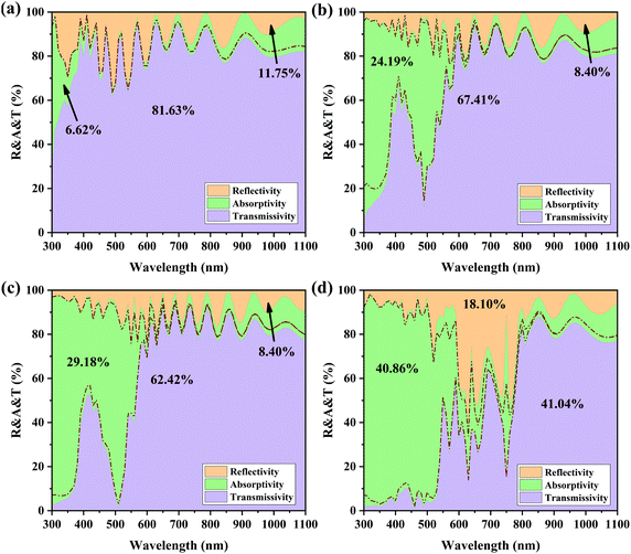
Helical SiNWs with wide spectral scattering are applied to translucent SiNW array solar cells. The solar cell structure is shown in Fig. 5a. This type of solar cell with cylindrical SiNWs has been prepared in experiments. Using Si micron wires, a PCE of nearly 9% can be obtained.19 The helical SiNWs and helical nanowires of other materials can also be prepared in the experiment.30–34 Therefore, it is possible to prepare translucent helical SiNW array solar cells in the experiment. The PEDOT:PSS film forms a heterojunction on the top of SiNWs. Light is incident from one side of PEDOT:PSS film and transmitted from the ITO side. The model used in the optical calculation of SiNW array solar cells is shown in Fig. 5b. The calculation details can be found in the ESI.†The reflectivity, absorptivity, and transmissivity of different SiNW array solar cells are shown in Fig. 6. The area of the dotted line and transmittance curve is the light absorption generated by the ITO film, and the area surrounded by the dotted line and reflectivity curve is the light absorption of the PEDOT:PSS film. These two parts of light absorption cannot produce carriers, which is called parasitic light absorption of the functional layer. Fig. 6a shows the reflectivity, absorptivity, and transmissivity spectra of solar cells without a SiNW array. At this time, the light absorption is parasitic light absorption, and there is less absorption without SiNWs. In the shortwave range, ITO films absorb more light, and with the increase in wavelength, the light absorption of PEDOT:PSS films increases gradually, and the total light absorption is 6.62%. Taking this as a reference, it can be found that the light absorption of translucent solar cells with SiNW arrays increases significantly, and the parasitic absorption generated by PEDOT:PSS films and ITO films decreases significantly. Fig. 6b shows the reflectivity, absorptivity, and transmissivity spectra of the cylindrical SiNW H array transparent solar cell. The light absorption of the SiNW array has an obvious absorption peak at the wavelength of 500 nm, which corresponds to the peak of a single SiNW here. With the increase in the height of SiNWs, the position of the peak has some redshift, and the intensity of the peak increases, but the overall characteristics have not changed. This is consistent with the optical properties of a single SiNW. When the SiNW array is a helical SiNW, the light absorption is very strong in the range of wavelength less than 550 nm, which is much higher than that of the SiNW array, as shown in Fig. 6d. When the wavelength is greater than 550 nm and less than 800 nm, there is partial light absorption, which widens the absorption spectrum compared with the cylindrical SiNW array. Finally, the light absorption of helical SiNWs is 40.86%, which is 40.02% higher than that of the cylindrical SiNW V array. This proved that the width response spectrum of a single SiNW can improve the light absorption of SiNW array solar cells. However, the period calculated here is 400 nm, which seems to be unfavourable to cylindrical SiNW arrays even at the same volume ratio. Therefore, we added four sets of calculations, which are the reflectivity, absorptivity, and transmissivity of cylindrical SiNW H and SiNW V arrays at the period of 200 and 300 nm. The results show that the light absorption of all cylindrical SiNW arrays is less than that of helical SiNW arrays, which is shown in the ESI.†
Using the optical results calculated in Fig. 6 and ESI,† the electrical model of a three-dimensional translucent SiNW array solar cell is established, which is a calculation form of a weak coupling of optical and electrical dual physical fields. The details of the model are in the ESI.† The current density–voltage curves of the three SiNW array solar cells are shown in Fig. 7, and the detailed electrical information parameters are shown in Table 1. Among them, 1, 2, and 3 of SiNW H and SiNW V are SiNW arrays with periods of 400 nm, 300 nm, and 200 nm, respectively. The period of the helical SiNW array is set to 400 nm. Fig. 7a is the current density–voltage curve of cylindrical and helical SiNW array solar cells, and the short-circuit current density (JSC), filling factor (FF), and open circuit voltage (VOC) obtained by the calculation are shown in Fig. 7b and c. The JSC of the two kinds of cylindrical SiNW array solar cells will increase with the reduction of the period, but the maximum value does not exceed that of the helical SiNW array solar cell. With the increase of period, the FF and VOC of cylindrical SiNW array solar cells decrease, and the maximum value is less than that of helical SiNW array solar cells. This is because SiNWs have different light capture capabilities. The VOC can be analysed by the following formula,
 | (4) |
| Solar cells | J SC (mA cm−2) | V OC (V) | FF (%) | η (%) | |
|---|---|---|---|---|---|
| SiNW H | 1 | 5.17 | 0.672 | 84.29 | 2.93 |
| 2 | 6.42 | 0.663 | 84.09 | 3.58 | |
| 3 | 7.77 | 0.647 | 83.79 | 4.21 | |
| SiNW V | 1 | 6.80 | 0.678 | 84.42 | 3.89 |
| 2 | 7.95 | 0.668 | 84.20 | 4.47 | |
| 3 | 9.43 | 0.652 | 83.88 | 5.16 | |
| Helical SiNW | 10.06 | 0.688 | 84.58 | 5.85 |
Detailed electrical output parameters of different SiNW array solar cells are shown in Table 1. With the shortening of the period, the PCE of cylindrical SiNW array solar cells increases gradually, which is mainly due to the enhancement of JSC. Even if the period length is reduced, the maximum PCE of cylindrical SiNW array solar cells is 5.16%, which is less than that of helical SiNW array solar cells. Although the photoelectric performance of cylindrical SiNW array solar cells with a small period has been calculated and better performance has been obtained, in order to fairly measure the performance improvement of helical SiNW array solar cells, the same period needs to be used for comparison. Cylindrical SiNW V 1 and helical SiNW adopt a period length of 400 nm for comparison. The JSC of helical SiNW array solar cell is 10.06 mA cm−2, which is 47.94% higher than that of SiNW V array solar cell of 6.80 mA cm−2. The increase in JSC is more obvious than that of light absorption. The VOC is 0.688 V, which is higher than the open circuit voltage of 0.678 V of cylindrical SiNW V, which is due to the gap caused by the light absorption of SiNWs. The PCE of the helical SiNW array solar cell is 5.85%, which is 50.38% higher than that of the SiNW V array solar cell, which is 3.89%. Due to the enhanced light absorption brought by the helical SiNW array, the current density is increased, and then the PCE is improved. Compared with cylindrical SiNWs, helical SiNWs are more suitable for translucent SiNW array solar cells.
Helical SiNWs have broadband extinction and scattering spectra. Compared with cylindrical SiNWs, the direct light absorption is reduced, but the light absorption in SiNW arrays is greatly improved. The light absorption of helical SiNWs at 500 nm can be further improved to be comparable to those of cylindrical SiNW. This requires further solutions and cannot be accomplished by simply increasing the length of SiNWs to improve the light absorption at this wavelength. According to this characteristic, it can be used not only in translucent SiNW array solar cells, but also in other flexible solar cells, or as antireflection films. Helical SiNWs can also be designed as axial or radial junction solar cells, which can give full play to the electrical advantages of SiNWs and be used as micro power supply in electrical components.35,36 In addition, in the calculation process of this work, it is also found that helical SiNWs have the selectivity of polarized light, which is similar to other helical nanowire structures and can be used in optical devices.
5. Conclusions
In this work, we designed a helical SiNW with an ultra-wide response spectrum and applied it to translucent SiNW array solar cells to improve light absorption. The photon management equation is used to design SiNWs to obtain a single helical SiNW with dual-peak in response spectrum. The positions of the two peaks can be controlled by the characteristic scale of helical SiNWs, which basically realizes the full coverage of the band gap of the Si material in the wavelength range of light absorption. The optical properties of helical SiNWs in the AM1.5G solar spectrum are analysed. Compared with cylindrical SiNWs, although the light absorption is reduced by 32.6%, the scattering and extinction are increased by 80.6% and 59.8%, respectively. This property makes helical SiNWs more suitable for improving light absorption in SiNW arrays. Finally, the helical SiNWs were applied to the translucent SiNW array solar cells, and the photoelectric properties of cylindrical SiNW array solar cells with different period lengths are studied. It has been proved that helical SiNW array solar cells have more advantages, and the light absorption was improved by 40.03% and the PCE was improved by 50.39%.Author contributions
Z. Gao contributed the idea of the work and all the calculation work. Q. Geng, Z. Wang, and T. Gao wrote the manuscript and checked the data. Y. Li, L. Chen, and M. Li revised the manuscript. All authors contributed to scientific discussions. M. Li provided the research platform and financial support.Conflicts of interest
There are no conflicts to declare.Acknowledgements
This work was supported by the National Natural Science Foundation of China (Grant no. 51772096, 51972110, 52072121 and 52102245), Beijing Science and Technology Project (Z181100005118002), Par-Eu Scholars Program, Science and Technology Beijing 100 Leading Talent Training Project, Huaneng Group Headquarters Science and Technology Project, Special Project (Phase I) of Offshore Wind Power and Smart Energy System Science and Technology (HNKJ20-H88), the Fundamental Research Funds for the Central Universities (2020MS023, 2020MS028) and the NCEPU “Double First-Class” Program.References
- T. B. Olsson, L. Abariute, L. Hrachowina, E. Barrigon, D. Volpati, S. Limpert, G. Otnes, M. T. Borgstrom and C. N. Prinz, Nanoscale, 2020, 12, 14237–14244 RSC.
- D. Parlevliet and P. Jennings, J. Nanopart. Res., 2011, 13, 4431–4436 CrossRef CAS.
- K. Teker, Sens. Actuators, A, 2014, 216, 142–146 CrossRef CAS.
- X. Q. Zeng, M. L. Latimer, Z. L. Xiao, S. Panuganti, U. Welp, W. K. Kwok and T. Xu, Nano Lett., 2011, 11, 262–268 Search PubMed.
- J. Maire, R. Anufriev, T. Hori, J. Shiomi, S. Volz and M. Nomura, Sci. Rep., 2018, 8, 4452 CrossRef PubMed.
- L. Balaghi, G. Bussone, R. Grifone, R. Hubner, J. Grenzer, M. Ghorbani-Asl, A. V. Krasheninnikov, H. Schneider, M. Helm and E. Dimakis, Nat. Commun., 2019, 10, 2793 CrossRef PubMed.
- R. Vismara, N. O. Lank, R. Verre, M. Kall, O. Isabella and M. Zeman, Opt. Express, 2019, 27, A967–A980 CrossRef CAS PubMed.
- Z. Liang, M. Su, H. Wang, Y. Gong, F. Xie, L. Gong, H. Meng, P. Liu, H. Chen, W. Xie and J. Chen, ACS Appl. Mater. Interfaces, 2015, 7, 5830–5836 CrossRef CAS PubMed.
- Y. Li, W. Liu, Y. Luo, M. Cui and M. Li, Opt. Express, 2018, 26, A19–A29 CrossRef CAS PubMed.
- N. Tavakoli and E. Alarcon-Llado, Opt. Express, 2019, 27, A909–A923 CrossRef CAS PubMed.
- X. Liu, Y. Da, B. Sun and Y. Xuan, Sol. Energy, 2019, 182, 1–8 CrossRef CAS.
- J. Zhang, Y. Zhang, F. Zhang and B. Sun, Appl. Phys. Lett., 2013, 102 Search PubMed.
- P. Krogstrup, H. I. Jørgensen, M. Heiss, O. Demichel, J. V. Holm, M. Aagesen, J. Nygard and A. Fontcuberta i Morral, Nat. Photonics, 2013, 7, 306–310 CrossRef CAS.
- Y. Li, M. Li, R. Li, P. Fu, B. Jiang, D. Song, C. Shen, Y. Zhao and R. Huang, Opt. Commun., 2015, 355, 6–9 CrossRef CAS.
- Y. Li, M. Li, R. Li, P. Fu, L. Chu and D. Song, Appl. Phys. Lett., 2015, 106, 091908 CrossRef.
- L. Yu, S. Misra, J. Wang, S. Qian, M. Foldyna, J. Xu, Y. Shi, E. Johnson and P. R. Cabarrocas, Sci. Rep., 2014, 4, 4357 CrossRef PubMed.
- F. Bai, M. Li, R. Huang, Y. Yu, T. Gu, Z. Chen, H. Fan and B. Jiang, J. Nanopart. Res., 2013, 15, 1915 CrossRef.
- P. Yu, J. Wu, S. Liu, J. Xiong, C. Jagadish and Z. M. Wang, Nano Today, 2016, 11, 704–737 CrossRef CAS.
- S. B. Kang, J. H. Kim, M. H. Jeong, A. Sanger, C. U. Kim, C. M. Kim and K. J. Choi, Light: Sci. Appl., 2019, 8, 121 CrossRef CAS PubMed.
- Z. Gao, T. Gao, Y. Chen, Q. Geng, G. Lin, Y. Li, L. Chen and M. Li, J. Phys. Chem. C, 2021, 125, 3781–3792 CrossRef CAS.
- Y. Li, M. Li, D. Song, H. Liu, B. Jiang, F. Bai and L. Chu, Nano Energy, 2015, 11, 756–764 CrossRef CAS.
- Z. Gao, G. Lin, Y. Zheng, N. Sang, Y. Li, L. Chen and M. Li, Photonics Res., 2020, 8, 995–1001 CrossRef CAS.
- Y. Li, M. Li, P. Fu, R. Li, D. Song, C. Shen and Y. Zhao, Sci. Rep., 2015, 5, 11532 CrossRef CAS PubMed.
- J. Tong, M. Zhang, S. Zhang, Y. Lei, M. Li, M. Qin and Y. Li, Opt. Commun., 2020, 454, 124515 CrossRef CAS.
- M. Hussein, M. F. Hameed, N. F. Areed, A. Yahia and S. S. Obayya, Opt. Lett., 2016, 41, 1010–1013 CrossRef CAS PubMed.
- Y. Li, M. Li, R. Li, P. Fu, T. Wang, Y. Luo, J. M. Mbengue and M. Trevor, Sci. Rep., 2016, 6, 24847 CrossRef CAS PubMed.
- K. T. Fountaine, C. G. Kendall and H. A. Atwater, Opt. Express, 2014, 22(Suppl 3), A930–940 CrossRef CAS PubMed.
- R. Paniagua-Dominguez, G. Grzela, J. G. Rivas and J. A. Sanchez-Gil, Nanoscale, 2013, 5, 10582–10590 RSC.
- Z. Gao, G. Lin, Y. Chen, Y. Zheng, N. Sang, Y. Li, L. Chen and M. Li, Sol. Energy, 2020, 205, 275–281 CrossRef CAS.
- H. Ma, R. Yuan, J. Wang, Y. Shi, J. Xu, K. Chen and L. Yu, Nano Lett., 2020, 20, 5072–5080 CrossRef CAS PubMed.
- J. K. Gansel, M. Thiel, M. S. Rill, M. Decker, K. Bade, V. Saile, G. von Freymann, S. Linden and M. Wegener, Science, 2009, 325, 1513–1515 CrossRef CAS PubMed.
- M. Esposito, V. Tasco, F. Todisco, A. Benedetti, I. Tarantini, M. Cuscuna, L. Dominici, M. De Giorgi and A. Passaseo, Nanoscale, 2015, 7, 18081–18088 RSC.
- M. Nakagawa and T. Kawai, J. Am. Chem. Soc., 2018, 140, 4991–4994 CrossRef CAS PubMed.
- C.-W. Chen, H.-W. Tsai, Y.-C. Wang, T.-Y. Su, C.-H. Yang, W.-S. Lin, Z.-H. Lin, J.-S. Huang and Y.-L. Chueh, J. Mater. Chem. A, 2019, 7, 11452–11459 RSC.
- S. Zhang, T. Zhang, Z. Liu, J. Wang, L. Yu, J. Xu, K. Chen and P. Roca i Cabarrocas, Nano Energy, 2021, 86, 106121 CrossRef CAS.
- H. Zhang, Y. Lei, Q. Zhu, T. Qing, T. Zhang, W. Tian, M. Lange, M. Jiang, C. Han, J. Li, D. Koelle, R. Kleiner, W. W. Xu, Y. Wang, L. Yu, H. Wang and P. Wu, ACS Nano, 2019, 13, 10359–10365 CrossRef CAS PubMed.
Footnote |
| † Electronic supplementary information (ESI) available. See DOI: 10.1039/d1ma00988e |
| This journal is © The Royal Society of Chemistry 2022 |

