 Open Access Article
Creative Commons Attribution 3.0 Unported Licence
Enhancing corona resistance in Kapton with self-assembled two-dimensional montmorillonite nanocoatings
Ming
Ren†
a,
Yifei
Wang†
 a,
Jingjing
Liu
bc,
Chao
Wu
ad,
Zaili
Hou
bc,
Antigoni
Konstantinou
a,
Jierui
Zhou
ad,
Hiep
Nguyen
a,
Jingjing
Liu
bc,
Chao
Wu
ad,
Zaili
Hou
bc,
Antigoni
Konstantinou
a,
Jierui
Zhou
ad,
Hiep
Nguyen
 ad,
Kerry
Davis-Amendola
 a,
Luyi
Sun
 *bc and
Yang
Cao
 *ad
*ad
aElectrical Insulation Research Center, Institute of Materials Science University of Connecticut, CT 06269, USA. E-mail: yang.cao@uconn.edu
bPolymer Program, Institute of Materials Science University of Connecticut Storrs, CT 06269, USA. E-mail: luyi.sun@uconn.edu
cDepartment of Chemical and Biomolecular Engineering University of Connecticut Storrs, CT 06269, USA
dDepartment of Electrical and Computer Engineering University of Connecticut Storrs, CT 06269, USA
First published on 4th April 2022
Abstract
Polymer dielectrics have been widely used in electrical and electronic systems for capacitive energy storage and electrical insulation. However, emerging applications such as electric vehicles and hybrid electric aircraft demand improved polymer dielectrics for operation not only under high electric fields and high temperatures, but also extreme conditions, for example, low pressures at high altitudes, with largely increased likelihood of electrical partial discharges. To meet these stringent requirements of grand electrifications for payload efficiency, polymers with enhanced discharge resistance are highly desired. Here, we present a surface-engineering approach for Kapton® coated with self-assembled two-dimensional montmorillonite nanosheets. By suppressing the magnitude of the high-field partial discharges, this nanocoating endows polymers with improved discharge resistance, with satisfactory discharge endurance life of 200 hours at a high electric field of 46 kV mm−1 while maintaining the surface morphology of the polymer. Moreover, the MMT nanocoating can also improve the thermal stability of Kapton®, with significantly suppressed temperature coefficients for both the dielectric constant and dielectric loss over a wide temperature range from 25 to 205 °C. This work provides a practical method of surface nanocoating to explore high-discharge-resistant polymers for harsh condition electrification.
1. Introduction
Polymer films have been widely used as dielectric media for insulation and charge storage in electronics and power systems for many years due to their excellent electrical and chemical stabilities, as well as their great processing scalability.1–8 The reliability and efficiency of many electrical apparatus are closely associated with the performance of polymer film dielectrics. To further extend the applications of polymers to extreme conditions such as ultrahigh electric field, excessive heat, and harsh environments, including undesirable corona corrosion and moisture exposure, various approaches have been developed to modify the existing specific polymers. For example, surface modifications, such as direct fluorination, oxyfluorination, and plasma treatments were applied to the polymer films for introducing a suppression effect on charge injection and increasing the flashover voltage.9–11 Besides, micro polymeric layers, such as polycarbonate/poly(vinylidene fluoride), were co-extruded to create a multi-layered film with a high dielectric strength and a high dielectric constant.12Among all the polymer modification methods, micro- and nano-polymeric composites containing inorganic fillers have attracted extensive and increasing research interest due to their potential enhancement in terms of electrical discharge resistance, treeing resistance, and dielectric strength.13–17 Montmorillonite (MMT), an important member of the natural inorganic 2![[thin space (1/6-em)]](https://www.rsc.org/images/entities/char_2009.gif) :
:![[thin space (1/6-em)]](https://www.rsc.org/images/entities/char_2009.gif) 1 smectite clay family, consists of a nano-dimensional layered structure that is similar to those of mica and talc. It can be fully exfoliated into single-layer nanosheets with a very high aspect ratio for the formation of highly structured nanocomposites.18,19 Incorporation of MMT nanosheets in the polymer matrix with proper surface modification, dispersion, and orientation can dramatically alter its thermal, mechanical, and dielectric properties for targeted performance enhancement.20 In addition to the application of MMT in nanocomposites, fully exfoliated MMT nanosheets can be self-assembled on the surface of polymers to form a coating with hundreds of layers of highly oriented and aligned laminar nanosheets.19 Such multi-functional coatings can be applied to various substrate films due to their excellent barriers against moisture, gas, and flame retardancy.21 From a manufacturing point of view, such a nanoclay coating is inexpensive to process and can be applied to a wide range of polymers.22 Unlike the microlayered polymer films achieved by coextrusion processing, this nanoclay coating can produce extremely high-density ordered organic/inorganic interfaces composed of nanosheets with a thickness of 1 nanometer, which can efficiently enhance the insulation property and long-term stability of the coated polymer films.23
1 smectite clay family, consists of a nano-dimensional layered structure that is similar to those of mica and talc. It can be fully exfoliated into single-layer nanosheets with a very high aspect ratio for the formation of highly structured nanocomposites.18,19 Incorporation of MMT nanosheets in the polymer matrix with proper surface modification, dispersion, and orientation can dramatically alter its thermal, mechanical, and dielectric properties for targeted performance enhancement.20 In addition to the application of MMT in nanocomposites, fully exfoliated MMT nanosheets can be self-assembled on the surface of polymers to form a coating with hundreds of layers of highly oriented and aligned laminar nanosheets.19 Such multi-functional coatings can be applied to various substrate films due to their excellent barriers against moisture, gas, and flame retardancy.21 From a manufacturing point of view, such a nanoclay coating is inexpensive to process and can be applied to a wide range of polymers.22 Unlike the microlayered polymer films achieved by coextrusion processing, this nanoclay coating can produce extremely high-density ordered organic/inorganic interfaces composed of nanosheets with a thickness of 1 nanometer, which can efficiently enhance the insulation property and long-term stability of the coated polymer films.23
In this study, to assess the endurance life imparted by such coatings in terms of harsh condition electrical insulation, we fabricated MMT self-assembly coatings on the surfaces of polyimide (PI) film (Kapton® HN), which is widely used in electrical power apparatus and electronics as dielectric coatings for copper wires/conductors, motor slot-liners, flexible circuit substrates, and dielectric thin films and encapsulation layers. Specifically, we evaluated the coating resistance enhancement to the electrical corona discharge, which represents the most stringent electrical extreme with not only high electric stress, but also intense electrical discharges and the associated local overheating. It is found that the discharge endurance lifetime of Kapton® HN can be significantly extended with the MMT coating, comparing favorably against Kapton® CR, a commercial grade of Kapton® specially designed for Corona Resistance (CR). Furthermore, electrical partial-discharge (PD) measurement, optical discharge imaging, and 3D profilometry analysis of the surface damage pattern were employed to reveal the mechanism of enhanced resistance properties. Extensive comparative studies of the different aging processes suggested a unique corona discharge withstanding imparted by these 2D MMT self-assembled coatings, whereas the anisotropic electrical conduction associated with these 2D MMT nanosheets suppresses effectively the formation of more dangerous streamer discharges. The resulting more uniform glow-like discharges can be favorably withstood by the superior barriers formed with the highly ordered and nanolayered-structure. The extrinsic nature of this self-assembled coating makes it readily applicable to a broad range of dielectric substrates, and with further tailoring, could satisfy the particular requirements of many electrical applications, especially the harsh condition electrifications and (hybrid) electric transportations.
2. Methods
2.1. Materials
Poly(vinyl alcohol) (PVA) (Mowiol® 8-88, Kuraray), sodium montmorillonite (MMT) (PGN nanoclay, Minerals Technologies Inc.), glutaraldehyde (GA, 50% aqueous solution, Aldrich), and HCl (37%, Aldrich) were used for the formation of the coatings. Kapton® HN polyimide (PI) films were employed as substrates for the coating study.2.2. Nanocoating preparation
PVA was dissolved in de-ionized (DI) water with the assistance of brief heating. MMT was uniformly dispersed in DI water with the assistance of stirring followed by brief ultrasonication in an ultrasonication bath (Branson 8510R-MT, 250 W, 44 kHz). After that, the PVA solution was added to the MMT aqueous suspension to form a dispersion system containing 1.5 wt% of total solids with a 1![[thin space (1/6-em)]](https://www.rsc.org/images/entities/char_2009.gif) :
:![[thin space (1/6-em)]](https://www.rsc.org/images/entities/char_2009.gif) 1 mass ratio of MMT/PVA. The mixture was stirred for 30 min and briefly ultrasonicated to achieve uniform dispersion. A small amount of crosslinking agent GA was added to the mixture. The molar ratio of GA to the total mole number of hydroxyl groups on the PVA chains was 1
1 mass ratio of MMT/PVA. The mixture was stirred for 30 min and briefly ultrasonicated to achieve uniform dispersion. A small amount of crosslinking agent GA was added to the mixture. The molar ratio of GA to the total mole number of hydroxyl groups on the PVA chains was 1![[thin space (1/6-em)]](https://www.rsc.org/images/entities/char_2009.gif) :
:![[thin space (1/6-em)]](https://www.rsc.org/images/entities/char_2009.gif) 20. HCl was also added as a catalyst for the crosslinking reaction at an HCl to GA molar ratio of 1
20. HCl was also added as a catalyst for the crosslinking reaction at an HCl to GA molar ratio of 1![[thin space (1/6-em)]](https://www.rsc.org/images/entities/char_2009.gif) :
:![[thin space (1/6-em)]](https://www.rsc.org/images/entities/char_2009.gif) 5.
5.
The polymer films (ca. 15 × 20 cm2) were facilely coated by dipping them into the above aqueous dispersion for ca. 10 seconds, and then vertically hung in an oven to be dried and crosslinked at 60 °C. The schematics of the nanocoating preparation procedures are shown briefly in Fig. 1a.
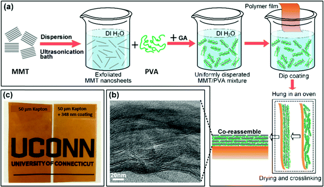 | ||
| Fig. 1 (a) Procedures of the formation of the MMT/PVA nanocoating and (b) TEM image of the cross-section of the coating layer. (c) Photo of the MMT-coated polymer film. | ||
In order to image the cross-section of the nanocoatings, the coated Kapton® HN films were embedded into epoxy and microtomed into thin slices with a thickness of ca. 100 nm on a Reichert-Jung Ultracut E ultramicrotome. The thin sections were deposited on copper grids for imaging in a JEOL JEM 1200EXII transmission electron microscope (TEM) with an accelerating voltage of 120 kV. As shown in Fig. 1b, the TEM image of the cross-section of the coating on a Kapton® HN film, the dispersed MMT nanosheets were coassembled with PVA on the substrate to form a highly ordered and oriented alternating laminate structure. It is worth mentioning that the transparency of the coated films was barely reduced even with a coating thickness of 348 nm (on both sides) due to the highly ordered nanostructure of the coating layers. The clarity of the “UCONN” logo underneath the coated film illustrates the film's transparency, as shown in Fig. 1c.
2.3. Experimental set-up
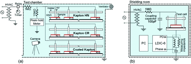
To assess the capabilities of the polymer films to withstand high electric field and corona discharge corrosion, comparative experiments regarding the corona endurance were carried out on both the blank and the MMT coated Kapton® HN films, along with a Kapton® CR baseline.3. Results
3.1. Insulation endurance under corona discharge conditions
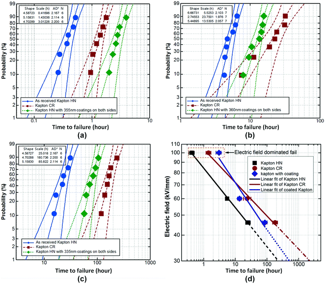
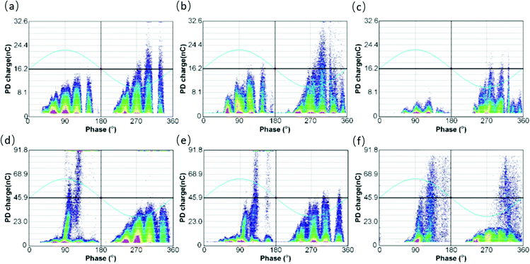
Corona resistance (or surface discharge resistance) testing is applied to assess insulating materials which are expected to be exposed to corona discharges in operation. In addition to the steady high field through the sample, a complex electrochemical aging effect is applied on the surface of the sample with the formation of surface electrical plasma discharges, involving attacks from energetic electrons and ions, and chemical damage by oxides, ozone, and water. The coating study was conducted over Kapton® HN, which is a common type of Kapton® for various applications in the physical, chemical, and electrical industries. In addition, we included also Kapton® CR as the baseline, a commercial product developed especially for working under (partial) electrical discharge environments in rail traction, industrial motors and generators, transformers, magnet wires, coils, and so on. For comparison, our coating was made on as received Kapton® HN film. Fig. 3a and c show the Weibull times to failure of the three Kapton films. Significant improvement of corona resistance has been found on the coated Kapton® HN film at the various applied voltage levels investigated. The Weibull times to failure of the coated Kapton® HN film at 6.25E0rms, 3.75E0rms, and 2.9E0rms (the corona inception field, E0rms = 16 kV mm−1, determined by PD detection) are 7.6, 3.1, and 3.5 times longer than those of the as-received blank film, respectively. Moreover, the coated Kapton® HN film can withstand the extremely intensive corona at a relatively high field (E0rms = 100 kV mm−1) for a longer time compared to the Kapton® CR film.The electrical aging of materials under corona conditions is closely related to the PD energy (pulse amplitude) released on the surface. Polymer chain scissions can take place due to the reactive impingements of the electrons, ions, and photons which have an energy higher than the binding energy. If the corona is relatively weak, a thermodynamic equilibrium can be established between the release and dissipation of discharge energy on the surface of the material; otherwise, the discharge energy is accumulated in local areas resulting in additional electrical-thermal damage. Moreover, the oxygen and the moisture in the air, and the ozone produced by discharges further accelerate the corona aging process. The corona withstanding capability is believed to be closely associated with the mode of PD energy release on the dielectric surface which can be changed by surface modification. Hence, the PD measurement can help us to understand the effect of nanocoating on the corona aging process. The phase-resolved partial discharge (PRPD) pattern, which is a powerful tool for PD analysis, was employed in this study.24 The PRPD patterns of the three Kapton films under relatively low and high fields are shown in Fig. 4. Most PDs are periodically distributed near both the positive and negative half cycles of the applied ac voltage. In the presence of the coating, the PDs are distributed in the narrower phase ranges with lower magnitudes under either relatively low field or extremely high field. A clear conclusion can be drawn from the PRPD statistics that under relatively low field, the PD events on Kapton® HN and Kapton® CR films with magnitude above 2.0 nC account for 38.2% and 35.6%, respectively, which are considerably greater than the percentage of the PDs (11.3%) on the coated Kapton® HN film with only PD with magnitude below the same level. Under extremely high field, the percentages of the PDs above 2.0 nC on the two uncoated Kapton® films (23.8% for Kapton® HN and 21.5% for Kapton® CR) are also greater than that on the coated film (9.1%). In general, with the presence of the 2D MMT coating, the PDs with great magnitude (energy) could be converted to an increased number of PDs with small magnitudes, which can be also proved by the recognizable PD emission features at various voltage conditions, as shown in Fig. 5.
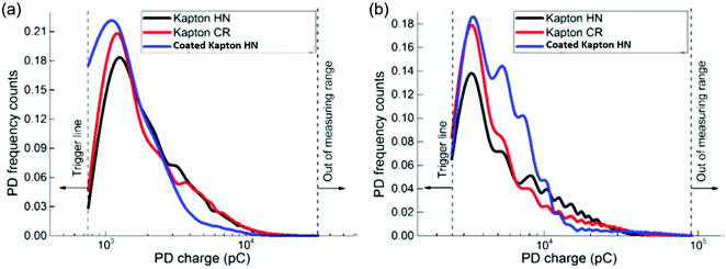 | ||
| Fig. 5 Distributions of PDs with PD charge under relatively low and high electric fields. (a) Under an electric field of 46 kV mm−1; (b) under an electric field of 100 kV mm−1. | ||
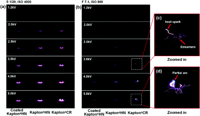
With the increase of the applied electric field, the faint avalanches in the vicinity of the electrode turn into photo ionization dominated streamers (see long exposure photo images shown in Fig. 6 with exposure settings as marked) and even thermal ionization dominated leaders (see Fig. 6c and d) which release intensive photons, charged particles and transient heat on the dielectric surface resulting in irreversible damage. In all the case studies with applied voltages ranging from 1.2 to 5.0 kV, it can be seen that the light emitted from the surface discharges on the MMT coated Kapton® films is less intensive and more uniform than those on Kapton® HN and CR films. This is attributed to the preferred anisotropic conductivity of 2D MMT, whose in-plane ionic conductivity suppresses the local field increment near the top electrode, thus leading to a reduced and more faint glow-discharge like pattern. It is interesting to reveal via the magnified images of the discharge photos of Kapton® HN and CR films that their discharge images are more branched in nature with the tendency to develop intermittently into bright spark discharges and for the case of Kapton® CR even partial arcs. As the spark discharges and particularly the arcing involve nearly fully developed thermal plasma with not only hot electrons but also hot ions, these discharges lead in general to much severe and rapid (surface) damaging of the dielectric films.
3.2. Damage patterns
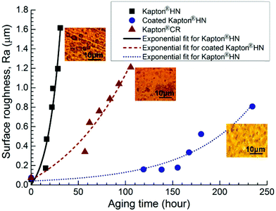
The numerous interfaces accompanied by the MMT coating layers not only help to dissipate the energy released on the dielectric surface retarding the propagation of discharge to a certain extent, but also protect the substrate film from the direct damage of the energetic particles generated from the partial discharges. The optical surface micrographs of the three types of films before and after corona aging are shown in Fig. 7. The significant differences in terms of the corrosion shape and extent can be observed between the virgin Kapton® HN and the coated Kapton® HN after corona aging for several hours. There are intensive pits and peaks formed on the surface of the Kapton® HN film after 13 hours of aging (see Fig. 7b). These pits gradually combine together and propagate into deeper (up to 6 μm) and more concentrated depressions after 20 hours of aging (see Fig. 8c). In the presence of the coating, shallow scratches instead of pits were observed on the surface of the coated Kapton® HN film after 47 h aging and 82 h aging (see Fig. 8e and f). The Kapton® CR film withstands the corona in a different way such that the damage traces are more dispersed and uniform on the surface, which is shown in its damage pattern (see Fig. 7h and i).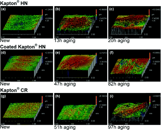 | ||
| Fig. 7 Images of corona aged zones of the three Kapton films subjected to 46 kV mm−1 field. All pictures were obtained by a 3D scanning profiler. | ||
The variations of the surface roughness of the three films with corona aging time are shown in Fig. 8. It indicates that the growth rate of the surface roughness of the coated film is significantly lower than that of the as-received one, which means that the nanoclay coating can retard the damage of the corona efficiently.
4. Discussion
Besides the damage of the continuous corona on the surface, the dielectric has to withstand the longitudinal component of the electric field through the whole dielectric, which is deemed to be a fatal factor in breakdown after a certain degree of corona corrosion. This is the reason why the corona endurance time of the coated Kapton HN film is even longer than that of the Kapton® CR film. If the applied electric field is relatively low, the longitudinal component no longer dominates the failure of the polymer film. In this case, the complex electrochemical processes are involved in corona-dominated degradation. Instead of the thermal decomposition which results in the reversion of polyimide into its monomers, the corona gives rise to the fracture and reorientation of the chemical bonds in polyimide chains. For example, the relaxed and reoriented bonds in polyimide such as C–N–C, C![[double bond, length as m-dash]](https://www.rsc.org/images/entities/char_e001.gif) O, benzene (C6Hn), ether link (C–O–C), and –OCH2–CH2 deformation have been observed by analysis of FTIR and Raman spectra after corona aging, which is attributed to the fact that the energy of the photons or electrons from the corona discharge are higher than the binding energy of the bond.25 This degradation is reflected in the changes in the surface morphology of the polymer film, e.g., the numerous crater-like pits on Kapton® HN where the electric field is concentrated. In the presence of the coating, the substrate film can be effectively protected from the direct attacks of the hot electrons and photon radiations from the discharges.
O, benzene (C6Hn), ether link (C–O–C), and –OCH2–CH2 deformation have been observed by analysis of FTIR and Raman spectra after corona aging, which is attributed to the fact that the energy of the photons or electrons from the corona discharge are higher than the binding energy of the bond.25 This degradation is reflected in the changes in the surface morphology of the polymer film, e.g., the numerous crater-like pits on Kapton® HN where the electric field is concentrated. In the presence of the coating, the substrate film can be effectively protected from the direct attacks of the hot electrons and photon radiations from the discharges.
The protection effect rendered by the nanoclay coating can be described macroscopically as the following perspectives:
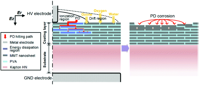
Once the initiatory effective electron is generated within the critical region of the electric field, the discharge occurs and propagates along the electric field line. MMT has relatively greater permittivity compared to the polymer, and hence the potential of the MMT nanosheet is relatively lower than that of the polymer, which makes the electric field more concentrated on the MMT nanosheet region. In this case, the PD is more inclined to be released on the MMT nanosheet, which has a stronger PD resistance compared to the polymer (PVA). The energetic electrons and photons caused by the discharges can be resisted effectively by the MMT layer owing to its very high aspect ratio. The numerous barriers extend the PD hitting path in PVA and increase the time to penetrate corrosion through the coating. In addition, the enhancement in surface conductivity due to the interface layers between the nanosheet and PI chain can shorten the decay time of charge on the dielectric surface, thus avoiding the dielectric from the more intensive discharges, such as leader and partial arc (see Fig. 9), occurring at the reversals of the applied potential from one half-cycle to the other. PDs degrade the polymer regions between the nanosheets selectively and even step aside from the nanosheets to intrude into their backsides. As the PVA interlayer is vaporized gradually by PD corrosion, MMT nanosheets are thus stacked layer by layer. Due to the high aspect ratio of the MMT nanosheet, the PD propagation path is extended dramatically along with the interfaces between the MMT layers. MMT layers, which have excellent PD resistance, release the most PD energy and protect the polymer substrate from the direct hitting of PDs.
Beyond that, the presence of oxygen and water that arises from the atmospheric moisture as well as the ozone from the corona will accelerate the degradation of polyimide with the effect of high temperature.26 Therefore, the endurance of the polymer under high electric stress can benefit from the significant gas and moisture barrier effects of the coating, which can retard the electrochemical aging process to a great extent.
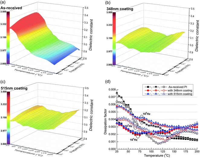
Admittedly, it has been indicated that the corona resistance of polymers can be improved by directly dispersing a certain amount of inorganic micro or nanoparticles such as TiO2,27 Al2O3,28 and MMT29 into the polymer, but this approach may give rise to more undesirable changes such as degraded breakdown strength, excessive dielectric loss, and even more internal defects. It should be noted that the dielectric response of our nanoclay coated film is also satisfactory. As shown in Fig. 10, at a frequency ranging from 20 to 106 Hz, the thermal stability in Dk was improved remarkably with the nanoclay coatings, as shown in Fig. 10a–c. Flat Dk responses were observed over the temperature range from 25 to 205 °C. For example, the maximal variation of the PI film with a 348 nm coating is 1.6% at 105 Hz while it is 13.5% for the as-received PI film at 105 Hz. No appreciable increase in DF values was observed in the PI films with 348 nm coating and 515 nm coating above 104 Hz, as shown in Fig. 10d.
5. Conclusions
In summary, we designed and demonstrated polymer films with self-assembled 2D MMT nanocoatings that possess significantly enhanced dielectric and electrical insulation properties. Suppressed partial discharges and elongated time-to-failure under high-field discharges were obtained after the MMT nanosheets were coated on the polymer surfaces. With 2D MMT self-assembly coatings, this approach endows a relatively high in-plane surface conductivity but maintains excellent insulation and blocking capabilities through the thickness direction, thus leading to less intensive surface discharge and well-preserved surface morphology. The coating layer also contributes to the enhancement in thermal stability, which can extend polymers applicable under harsh conditions. With further tailoring, this surface engineering method can be utilized in the modification of a wide range of dielectric materials for emerging harsh condition electrifications such as hybrid-electric passenger airplanes and electric cars.Author contributions
M. R. and Y. W. contributed equally to this work. L. S. and Y. C. conceived the idea. J. L. and Z. H. prepared the nanocoatings and conducted most of the characterizations of the nanocoatings. M. R., Y. W., C. W., A. K., J. Z., H. N., and K. D. carried out electrical characterizations. M. R., Y. W., Y. C., and L. S. wrote the first draft of the manuscript. All authors contributed to revising the manuscript.Conflicts of interest
There are no conflicts to declare.Acknowledgements
Y. C. acknowledges the support by the National Science Foundation (1650544), the Office of Naval Research (N00014-19-1-2306), and the Army Research Lab (W911NF-16-2-0146). L. S. acknowledges the support by the National Science Foundation (CMMI-1562907).Notes and references
- X. Zhang, X. Zhang, M. Yang, S. Yang, H. Wu, S. Guo and Y. Wang, Compos. Sci. Technol., 2016, 136, 104–110 CrossRef CAS.
- C. Wu, A. A. Deshmukh, Z. Li, L. Chen, A. Alamri, Y. Wang, R. Ramprasad, G. A. Sotzing and Y. Cao, Adv. Mater., 2020, 32, e2000499 CrossRef PubMed.
- Y. Lin, C. Sun, S. Zhan, Y. Zhang and Q. Yuan, Adv. Mater. Interfaces, 2020, 7, 2000033 CrossRef CAS.
- G. Liu, Y. Feng, T. Zhang, C. Zhang, Q. Chi, Y. Zhang, Y. Zhang and Q. Lei, J. Mater. Chem. A, 2021, 9, 16384–16394 RSC.
- Q. Li, L. Chen, M. R. Gadinski, S. Zhang, G. Zhang, U. Li, E. Iagodkine, A. Haque, L. Q. Chen, N. Jackson and Q. Wang, Nature, 2015, 523, 576–579 CrossRef CAS PubMed.
- B. Chu, X. Zhou, K. Ren, B. Neese, M. Lin, Q. Wang, F. Bauer and Q. M. Zhang, Science, 2006, 313, 334–336 CrossRef CAS PubMed.
- J. Chen, Y. Wang and W. Chen, J. Mater. Chem. C, 2021, 9, 5000–5007 RSC.
- J. Dong, R. Hu, X. Xu, J. Chen, Y. Niu, F. Wang, J. Hao, K. Wu, Q. Wang and H. Wang, Adv. Funct. Mater., 2021, 31 Search PubMed.
- A. Kharitonov, Prog. Org. Coat., 2008, 61, 192–204 CrossRef CAS.
- S. Schlögl, R. Kramer, D. Lenko, H. Schröttner, R. Schaller, A. Holzner and W. Kern, Eur. Polym. J., 2011, 47, 2321–2330 CrossRef.
- F. Kong, C. Chang, Y. Ma, C. Zhang, C. Ren and T. Shao, Appl. Surf. Sci., 2018, 459, 300–308 CrossRef CAS.
- M. Mackey, D. E. Schuele, L. Zhu, L. Flandin, M. A. Wolak, J. S. Shirk, A. Hiltner and E. Baer, Macromolecules, 2012, 45, 1954–1962 CrossRef CAS.
- D. Fabiani, G. Montanari, A. Cavallini, A. Saccani and M. Toselli, Proceedings of 2011 International Symposium on Electrical Insulating Materials, 2011, pp. 16–19 Search PubMed.
- S. Nunes and M. Shaw, IEEE Trans. Electr. Insul., 1980, 437–450 CAS.
- T. Linker, Y. Wang, A. Mishra, D. Kamal, Y. Cao, R. K. Kalia, A. Nakano, R. Ramprasad, F. Shimojo and G. Sotzing, ACS Appl. Mater. Interfaces, 2021, 13, 60393–60400 CrossRef CAS PubMed.
- Z. Pan, L. Yao, J. Zhai, X. Yao and H. Chen, Adv. Mater., 2018, 30, 1705662 CrossRef PubMed.
- Y. Zhu, Y. Zhu, X. Huang, J. Chen, Q. Li, J. He and P. Jiang, Adv. Energy Mater., 2019, 9, 1901826 CrossRef.
- Y. Wang, S. Nasreen, D. Kamal, Z. Li, C. Wu, J. Huo, L. Chen, R. Ramprasad and Y. Cao, ACS Appl. Mater. Interfaces, 2021, 13, 46142–46150 CrossRef CAS PubMed.
- S. P. Fillery, H. Koerner, L. Drummy, E. Dunkerley, M. F. Durstock, D. F. Schmidt and R. A. Vaia, ACS Appl. Mater. Interfaces, 2012, 4, 1388–1396 CrossRef CAS PubMed.
- Y. Wang, Z. Li, C. Wu and Y. Cao, Chem. Eng. J., 2020, 401, 126093 CrossRef CAS.
- F. Ding, J. Liu, S. Zeng, Y. Xia, K. M. Wells, M. P. Nieh and L. Sun, Sci. Adv., 2017, 3, e1701212 CrossRef PubMed.
- B. Zhang, J. Liu, M. Ren, C. Wu, T. J. Moran, S. Zeng, S. E. Chavez, Z. Hou, Z. Li and A. M. LaChance, Adv. Mater., 2021, 2101374 CrossRef CAS PubMed.
- D. Langhe and M. Ponting, Manufacturing and novel applications of multilayer polymer films, William Andrew, 2016 Search PubMed.
- A. Cavallini, G. Montanari, F. Puletti and A. Contin, IEEE Trans. Dielectr. Electr. Insul., 2005, 12, 203–215 CrossRef.
- Y. Yang, D. Yin, R. Xiong, J. Shi, F. Tian, X. Wang and Q. Lei, IEEE Trans. Dielectr. Electr. Insul., 2012, 19, 574–581 CAS.
- Y. Luo, G. Wu, J. Liu, J. Peng, G. Zhu and G. Gao, IEEE Trans. Dielectr. Electr. Insul., 2014, 21, 1824–1834 CAS.
- J. Zha, G. Chen, Z. Dang and Y. Yin, J. Electrost., 2011, 69, 255–260 CrossRef CAS.
- H. Li, G. Liu, B. Liu, W. Chen and S. Chen, Mater. Lett., 2007, 61, 1507–1511 CrossRef CAS.
- M. T. Jafari, M. Saraji and H. Sherafatmand, Anal. Chim. Acta, 2014, 814, 69–78 CrossRef CAS PubMed.
Footnote |
| † Theses authors contributed equally to this work. |
| This journal is © The Royal Society of Chemistry 2022 |

