 Open Access Article
Creative Commons Attribution 3.0 Unported Licence
Effect of van der Waals stacking in CdS monolayer on enhancing the hydrogen production efficiency of SiH monolayer
Francis
Opoku
 *a,
Albert
Aniagyei
 b,
Osei
Akoto
 a,
Edward Ebow
Kwaansa-Ansah
 a,
Noah Kyame
Asare-Donkor
 a and
Anthony Apeke
Adimado
 a
a
aDepartment of Chemistry, Kwame Nkrumah University of Science and Technology, Kumasi, Ghana. E-mail: ofrancis2010@gmail.com; francisopoku@knust.edu.gh
bDepartment of Basic Sciences, University of Health and Allied Sciences, Ho, Ghana
First published on 20th April 2022
Abstract
Photocatalytic water splitting for the generation of hydrogen can be achieved by utilizing highly efficient type II van der Waals (vdW) heterostructures as a novel class of materials with a highly tunable bandgap energy and band alignment. Herein, we constructed a CdS/SiH vdW heterostructure by stacking CdS on the top of SiH monolayers and investigated its potential application as a photocatalyst for water splitting using first-principles calculations. The results indicated that a stable interface with vdW interactions can be formed between the CdS and SiH monolayers based on phonon dispersion and AIMD simulations. The CdS/SiH vdW heterostructure is an indirect bandgap semiconductor with a type II band alignment, allowing the effective separation of photoexcited electron–hole pairs. In addition, the very large electrostatic potential drop (14.59 eV) across the CdS and SiH interface is expected to hinder the recombination of electron–hole pairs, and hence promote efficient photocatalytic activity. Besides, compared with the isolated CdS and SiH monolayers, the CdS/SiH vdW heterostructure has a broad absorption edge in the high-energy visible light region. Furthermore, the bandgap energy and band alignment of this heterostructure could be modified by applying biaxial strain and an external electric field. Thus, our study showed that the CdS/SiH heterostructure with vdW interactions has excellent optical and electronic properties with great potential as a high-performance solar-driven photocatalyst for the water splitting reaction and nanoelectronic and optoelectronic devices.
I. Introduction
It is well known that petroleum is the most frequently used energy source globally. However, the environmental problems caused by fuel exhaust gas are becoming more serious.1,2 Exhaust gases produced by the combustion of sulphur- and nitrogen-containing compounds in petrochemical fuels are comprised of photochemical smog, air pollutants, and acid rain components, which all have serious effects on the ecosystem and human health.3 Catalytic hydrogenation is commonly used to remove nitrogen-containing molecules from gasoline.4 However, traditional techniques of fuel denitrification have certain limitations, such as catalytic hydrogenation denitrification, which demands extremely high pressure and temperature, together with high energy costs and expensive manufacturing equipment.4 Hydrogen gas (H2), with its zero CO2 emissions and high energy density (∼122 kJ g−1), has received significant attention as a viable replacement to fossil fuels.5 However, H2 is mainly produced by refinery operations from the hydrocracking of fossil fuels, which is an environmentally unsustainable and energy-intensive method.6 Accordingly, the use of solar energy to produce hydrogen and oxygen via photocatalytic water splitting is one of the most promising ways to produce renewable and clean energy to meet future energy demands.7,8 Photocatalysis technology is one of the most promising routes to address environmental problems,9 which has several benefits compared to other solutions, such as high efficiency, environmental protection, direct use of sunlight at room temperature and good selectivity.10,11Several studies have been undertaken since the discovery of graphene to examine potential two-dimensional (2D) photocatalysts for water splitting,12–14 such as MXenes, Janus MAB (M = Mo and W; A and B = S, Se and Te), graphitic carbon nitrides (g-C6N6, g-C3N4 and C2N), group-III (IV) monochalcogenides, boron nitride, and transition-metal dichalcogenides.15–18 Due to their exceptional chemical and physical properties, as well as their great performances in a variety of applications, 2D materials have recently attracted widespread attention.19,20 Furthermore, 2D structures have a large surface area to volume ratio, allowing the creation of additional photocatalytic reaction sites and low recombination rate of charge carriers, resulting in their migration to the surface.21,22 Silicene, a 2D hexagonal lattice of silicon monolayer predicted theoretically in 2007 and synthesised in 2010,23 possesses the majority of superb electronic properties of graphene. Covalent modification of hydrogen and silicene, called silane (SiH), can result in a substantial bandgap in the Brillouin zone, analogous to that of graphene.24,25 Hydrogenation removes the conductivity of silicene and creates more stable structures, resulting in a small bandgap in the visible light region, which can be used for photocatalysis. Several studies have shown that SiH has a suitable indirect bandgap and a stable structure.26 Fully hydrogenated silicene is a good heterojunction composite material and has also been studied experimentally and theoretically.27,28 Because the highly reactive Si–H bonds may be used directly as reducing agents or reactants in chemical processes, they are of particular interest.29 Because of the distinctive electronic structures of the conduction band (CB) and valence band (VB) of silane, it is considered a viable choice as a photocatalyst.30 The use of a suitable cocatalyst is an efficient technique to improve the photocatalytic performance of materials.31 CdS is less expensive than noble metals and can absorb visible light,32 making it an excellent cocatalyst.33 CdS has been successfully synthesised through colloidal and solvothermal methods.34 CdS is a typical photocatalyst, which is widely employed in the production of H235 due to its excellent catalytic activity, good stability, sensitivity to solar-light irradiation, excellent electron transport and mobility properties.36 Solar cells based on CdS thin films have achieved an 80% fill factor, which has not been demonstrated with any other materials.37–39 Then, as a photodetector, multilayer cadmium-based devices exhibit high performances.40 Also, the CB edge of CdS is sufficiently negative compared to the redox potential of H2O/H2, making water reduction energetically viable.41
In recent years, research has focused on the use of 2D materials as viable photocatalysts for water splitting, which requires a longer photogenerated carrier lifetime.42,43 However, despite their promising chemical and physical features, monolayer 2D materials exhibit a low quantum efficiency in photocatalysis due to their short carrier lifetime induced by photogenerated charge transfer. Consequently, the search for materials with low cost, low lattice mismatch and activity to develop efficient photocatalysts has become an intriguing research topic. It has been reported that van der Waals force (vdWs) heterojunctions made of 2D materials present excellent photocatalytic water splitting performances to produce H2 because the weak vdWs force can combine various materials while maintaining the excellent inherent properties of the individual 2D monolayers.44,45 The photocatalytic efficiency can be improved using type II vdWs heterostructures46–50 to separate photogenerated electron–hole pairs into two distinct materials.51,52 Consequently, when a type II heterostructure is formed, the built-in electric field increases the spatial separation of charge carriers in the two separate 2D materials, increasing the photocatalytic quantum efficiency.53,54 To boost the photocatalytic performance of a 2D SiH layer, it was proven that SiH-based vdW type II heterostructures, such as SiH/TiO2,55 GaAs/SiH,56 InSe/SiH57 and PtSe2/SiH,15 which have been theoretically predicted to be excellent photocatalytic materials, can split water into H2 under solar irradiation. CdS-Based vdWs heterostructures exhibit super-high piezoelectricity, which have potential for the fabrication of 2D excitonic solar cells.58
Current research is focused on developing low-cost solar energy materials that are expected to produce the desired photocatalytic performance, such as compatible bandgap energies, high charge carrier lifetime and absorption of visible light energy.59 Considering the high photocatalytic activity of SiH and CdS monolayers and their high lattice matching, CdS/SiH vdWs heterostructures may be good visible-light-driven materials and outstanding photocatalysts for water splitting. Herein, a CdS/SiH vdW heterostructure was designed by vertically stacking CdS and SiH monolayers through vdW forces. The unique band edge positions of the CdS and SiH monolayers imply that a typical type II heterostructure may be formed between them. Based on first-principles calculations, we explored the charge transfer, optical absorption, electronic and structural properties, and the practicality of the CdS/SiH vdW heterostructure as an excellent photocatalyst for water splitting. The optimised structures of the CdS and SiH monolayers were initially studied. The stable structure and the vdWs force between layers were verified by calculating the phonon dispersion and electron localisation functions. The effects of biaxial strains and external electric field on the electronic and structural properties of the CdS/SiH vdW heterostructure were also thoroughly investigated. Löwdin charge population analysis and charge density difference were employed to examine the interfacial charge transfer.
II. Computational details
The PWscf code in the Quantum Espresso package60 was used to perform DFT and AIMD calculations based on the plane-wave basis set and optimised norm-conserving Vanderbilt pseudopotentials.61 The valence electron configurations of S (3s2 3p4), Cd (4d10 5s2) and Si (3s2 3p2) were considered. For electron exchange–correlation interactions, the generalised gradient approximation (GGA) established by Perdew–Burke–Ernzerhof62 was used to optimise the lattice structures. To account for the vdW interaction at the interface of the CdS/SiH heterostructure, the Grimme DFT-D3(BJ) dispersion method was used.63,64 The kinetic energy cutoff of 45 and 400 Ry was used for the plane-wave expansion and charge density, respectively. The Brillouin zone of the PWscf calculation was sampled using the Monkhorst–Pack scheme,65 where a uniform k-point mesh of 10 × 10 × 1 for the CdS monolayer and 13 × 13 × 1 for the SiH monolayer and CdS/SiH vdW heterostructure was used for the electronic property and relaxation calculations. The conjugate gradient method was used to compute the lattice convergence criterion until the energy and force were less than 10−8 Ry and 10−3 Ry bohr−1, respectively. For accurate optical and electronic property calculations, the hybrid Heyd–Scuseria–Ernzerhof functional66 was used. We ensured that a vacuum space of 20 Å along the z-direction was enough to eradicate interactions between neighbouring slabs. The dipole correction approach was used to adjust the periodic boundary condition inaccuracies in the atomic forces, electrostatic potentials and total energies.67 The amount of charge transfer was calculated using the Löwdin charge population analysis.68 The finite-displacement approach was used to determine the vibrational properties of the optimised structures using the density functional perturbation theory,69 as implemented in the Quantum Espresso package.60 AIMD simulations in the NVT ensemble at 300 K for 25 ps with a time step of 1 fs were performed to test the thermal stability of the CdS/SiH vdW heterostructure. The Nosé–Hoover thermostat was used to regulate the temperature.70III. Results and discussion
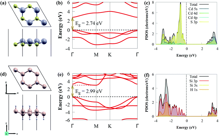
Before studying the photocatalytic properties of the CdS/SiH vdW heterostructure, we first explored the electronic properties and geometric structures of isolated CdS and SiH monolayers to test the accuracy of our calculations. The optimised structures (top and side views) of the CdS and SiH monolayers are presented in Fig. 1(a) and (d), respectively.After full structural optimisation, the lattice parameters of CdS and SiH were calculated to be 4.16 and 3.91 Å, respectively, which are highly consistent with earlier theoretical and experimental studies.57,71 The Si–H and Si–Si bond lengths are 1.50 and 2.37 Å, respectively, while the Cd–S bond length is 2.56 Å. We observed that the CdS and SiH monolayers have a direct and indirect bandgap, with values of 2.74 and 2.99 eV (Fig. 1(b) and (e)), respectively. The valence band maximum (VBM) and conduction band minimum (CBM) of the CdS monolayer are located at the Γ point, while the CBM and VBM of SiH are positioned at the Γ and M points, respectively. The partial density of states (PDOS) of the CdS monolayer shows that the VBM is dominantly composed of S 3p states, whereas the CBM is mostly dominated by the Cd 5s states (see Fig. 1(c)). The VBM mainly originates from the Si 3p states, whereas the CBM is composed of Si 3s and 3p states (Fig. 1(f)). These observations are completely in accordance with previous studies.12,29
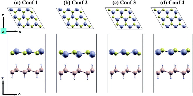
We used a unicell of CdS monolayer to match a unicell of SiH monolayer to form a highly symmetric unicell with a small lattice mismatch of −3.09%. In the unicell, the negative sign reflects the small lattice constant of the SiH monolayer with respect to the CdS monolayer. Mechanical strain can be induced on the CdS/SiH vdW heterostructure by compressing or stretching the unit cell of CdS or SiH, respectively. These 2D materials can be stacked in several ways to generate CdS/SiH vdW heterostructures. To evaluate the stability of the CdS/SiH vdW heterostructure, we looked at four different configurations, each of which is illustrated in Fig. 2.
All the configurations were fully relaxed using both force and energy convergence criteria. To determine the structural stability between the CdS and SiH monolayers, the binding energies (Eb) of the CdS/SiH vdW heterostructure in different configurations were evaluated using the following equation:
| Eb = (ECdS/SiH − ECdS − ESiH)/S, | (1) |
| Structure | a = b (Å) | E b (meV Å−2) | d (Å) | E g (eV) | Band nature |
|---|---|---|---|---|---|
| Conf1 | 4.076 | −5.88 | 3.776 | 2.78 | Direct |
| Conf2 | 4.059 | −9.75 | 3.173 | 2.07 | Indirect |
| Conf3 | 4.061 | −4.26 | 3.756 | 2.71 | Direct |
| Conf4 | 4.058 | −5.05 | 3.509 | 2.43 | Indirect |
As shown in Table 1, the binding energies and equilibrium interlayer distances in the CdS/SiH vdW heterostructure range from −4.26 to −9.75 meV Å−2 and 3.173 to 3.776 Å, respectively, indicating that van der Waals interactions occur in these four configurations. Generally, the most stable system has the shortest equilibrium interlayer distance, and only the most energetically favourable configuration is most likely to be synthesised. Stacking conf2 with the shortest interlayer distance of 3.173 Å possessed the lowest Eb, which makes it the most stable configuration among the stacking configurations. Therefore, we only considered stacking conf2 as the desired stacking pattern to further demonstrate the electronic and photocatalytic properties.
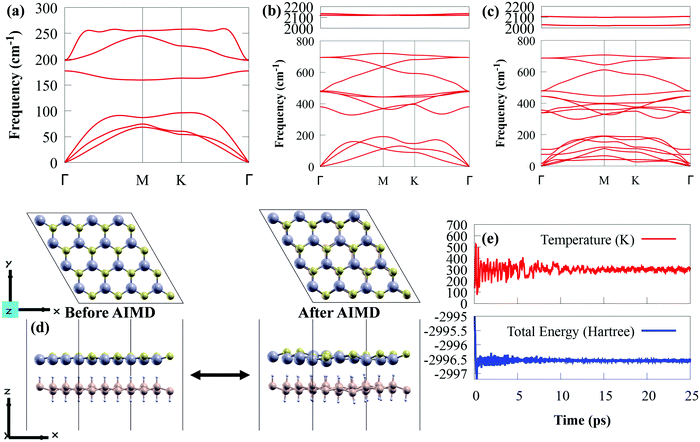
To explore the dynamic stability, the phonon spectra of SiH, CdS and CdS/SiH vdW heterostructure were obtained, as presented in Fig. 3(a)–(c), respectively. The CdS and SiH monolayers contain two and four atoms in their unit cell, respectively. Both the CdS and SiH monolayers have 3 acoustic phonon modes, and three and nine optical phonon modes, respectively. The CdS/SiH vdW heterostructure with six atoms in its unit cell has seven acoustic phonon modes and nine optical phonon modes. Clearly, the positive frequency modes throughout the Brillouin zone show that SiH, CdS and CdS/SiH vdW heterostructure maintain high thermodynamic stability at ambient temperature.
Subsequently, the thermal stability of a 4 × 4 supercell of the CdS/SiH vdW heterostructure was investigated using AIMD simulations at 300 K and the results are shown in Fig. 3(d). The CdS/SiH vdW heterostructure can keep its structure intact with no bond breaking within 25 ps, indicating that the CdS monolayer strongly interacts with the SiH monolayer. As shown in Fig. 3(e), there are no drastic variations in the ion temperature and potential energy, confirming that the CdS/SiH vdW heterostructure is thermally stable.
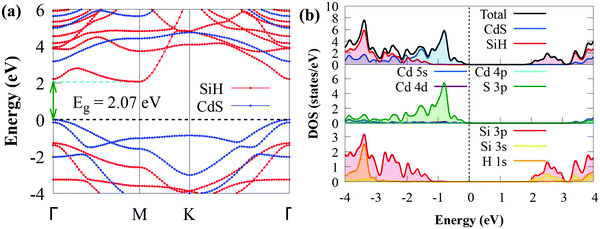
After establishing the stable configuration, we shifted our attention to the electronic properties of the CdS/SiH vdW heterostructure. The projected band structure, density of states (DOS) and PDOS were calculated using the HSE06 hybrid functional and the results are illustrated in Fig. 4.
As shown in Fig. 4(a), the CdS/SiH vdW heterostructure has an indirect bandgap of 2.07 eV, which is smaller than that of the monolayers, implying that the formation of the heterostructure can efficiently narrow the bandgap energy and electrons transfer more easily from the valence band (VB) to the conduction band (CB) of the CdS/SiH vdW heterostructure. The band structure of the heterostructure is almost an overlap of the energy bands of the two monolayers due to the comparatively weak interaction force; hence, the band distribution remained nearly unaltered. The PDOS reveals that the VBM of the CdS/SiH vdW heterostructure is dominated by S atoms in the CdS monolayer. In contrast, the CBM is dominated by Si atoms in the SiH monolayer, indicating that the VBM and CBM states are effectively separated. Under visible light irradiation, electrons are mostly transferred from the S 3p states to the Si 3p and Si 3s states during the photocatalytic process. Consequently, this indicates that CdS/SiH is a type II vdW heterostructure. Then, we may deduce that the water reduction and oxidation processes take place mostly in the SiH and CdS monolayers, respectively, which is favourable for the efficient separation of photogenerated charge carriers, improving the photocatalytic performance.
The three-dimensional and the planar averaged charge density difference in the z-direction were worth investigating to understand the binding mechanism and interfacial interactions of the CdS/SiH vdW heterostructure. A negative (positive) value represents charge depletion (accumulation). The charge density difference is considered as follows:72
| Δρ = ρCdS/SiH − ρCdS − ρSiH | (2) |
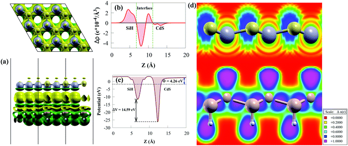
As illustrated in Fig. 5(a), we discovered that charge density redistribution and charge transfer between the SiH and CdS monolayers are possible. According to the above analysis, electrons transfer from the CdS monolayer to the SiH monolayer and accumulate on the SiH surface, while holes accumulate on the CdS surface, resulting in a built-in potential pointing from CdS to SiH at the CdS/SiH vdW heterostructure interface. We plotted the plane-averaged charge density difference to further confirm the interfacial charge, as shown in Fig. 5(b). A small charge of about 0.765 |e| can generate dipoles across the whole surface, resulting in a built-in electric field. It can be seen that the CdS monolayer has a deeper potential than the SiH monolayer due its exceptional flexibility and out-of-plane piezoelectricity,73 as depicted in Fig. 5(c). This causes electrons to transfer from the CdS monolayer to SiH monolayer, while the transfer of holes is the opposite. The charge transfer is substantial enough to provide a high potential drop (ΔV) of 14.59 eV (see Fig. 5(c)) between the SiH and CdS monolayers, resulting in a built-in electric field, thereby minimising photogenerated electron–hole pair recombination. Therefore, the large ΔV effectively enhances the separation and transfer of charge carriers.
We calculated the electron localisation function (ELF) to examine the bonding mechanism between the SiH and CdS monolayers. The magenta area (value of 1) means that electrons are highly localised in that region, while the red area (value of 0) in Fig. 5(d) indicates low electron localisation.74 It can clearly be seen that the ELF is close to zero at the interface, indicating that vdW force exists between the monolayers. This agrees with the binding energy and the layer spacing results.
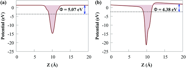
Charge transfer occurs across the interface due to the electron potential difference, which is defined by the work function (Φ) when two 2D monolayers are stacked together by vdW forces to produce a heterostructure. Consequently, Φ may depict the underlying mechanism of charge transfer between two 2D monolayers. Moreover, the work function of a photocatalyst material is a crucial variable, which is usually used as an essential reference to access the band alignment of semiconductors.75 The Φ of the CdS/SiH vdW heterostructure and SiH and CdS monolayers was calculated as follows:
| Φ = Evac − EF | (3) |
The Φ of the SiH and CdS monolayers agree with the previous study (5.147 eV for SiH).56 Because SiH has a larger Φ than CdS, the Φ difference causes electrons to transfer from the CB of CdS to the CB of SiH and holes to accumulate on the VB of SiH, which agree with the charge density difference results. Charges will continue to flow between the layers until their Fermi levels equalize. When charge builds on the monolayer surface, a built-in electric field is formed. This generates charge transfer resistance until the built-in electric field is large enough to balance the charge transfer. Moreover, the lower Φ value of the CdS/SiH vdW heterostructure than that of CdS and SiH signifies that charge transfer occurs at the interface.
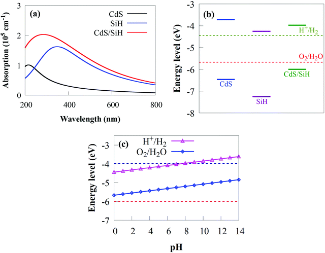
In addition to band edges and appropriate bandgaps, wide optical absorption in the visible light region is key to determine the photocatalytic performance of a material. Ideally, suitable visible light photocatalysts should have a bandgap energy between 1.9 and 2.3 eV.56 The predicted bandgap of the CdS/SiH vdW heterostructure is 2.07 eV, indicating that it can efficiently absorb visible light. To explore the combined effects of CdS and SiH, the optical absorption spectra of the CdS/SiH vdW heterostructure, CdS and SiH were calculated using hybrid HSE06 and TDDFT calculations.77,78 As shown in Fig. 7(a), the visible light absorption efficiency of the CdS monolayer is extremely low. However, the SiH monolayer outperforms the CdS monolayer. The absorption intensity and edge of the CdS/SiH vdW heterostructure in the ultraviolet and visible area are much higher than that of the SiH monolayer. The increased optical absorption intensity is generated by SiH and the reduced bandgap energy and interlayer coupling between the two monolayers. Consequently, it can be expected that the CdS/SiH vdW heterostructure with a suitable bandgap energy and good absorption edge redshift may be an outstanding candidate for application of electronic and optoelectronic devices.
Although all the foregoing investigations indicate that CdS/SiH is a staggered type II vdW heterostructure with high photocatalytic performance, its capacity to effectively split water to create H2 needs to be investigate. The water reduction potential (VH+/H2) and oxidation potential (VO2/H2O) must overlap the VBM and CBM potentials of 2D materials for them to be used as efficient photocatalysts for water splitting to create H2.79VO2/H2O and VH+/H2 are −5.67 and −4.44 eV relative to the vacuum level, respectively.79 The absolute energy positions of the VBM and CBM with regard to the vacuum level are critical to acquire the band edges of CdS, SiH and the CdS/SiH vdW heterostructure with respect to water electrode potential. DFT calculations were used to obtain the band edge potentials of the monolayers and the vdW heterostructure relative to the normal hydrogen electrode (ENHE). The absolute energy positions of the VBM and CBM were considered by shifting the vacuum level to the absolute vacuum energy scale (EAVS), as given in Fig. 7(b). The estimated EAVS is based on the following relationship: EAVS = −ENHE − 4.5. The VBM (CBM) potentials are −7.25 (−4.26), −6.46 (−3.72) and −6.05 (−3.97) eV for SiH, CdS and the CdS/SiH vdW heterostructure, respectively. The calculated CBM and VBM is 0.72 and 0.79 eV higher and lower than the water reduction and oxidation potentials, respectively, demonstrating that CdS has water splitting capacity. The VBM (CBM) of SiH is 1.58 eV (0.18 eV) lower (higher) than the water oxidation (reduction) potential, showing that although it has a larger bandgap than CdS, SiH possesses appropriate band edges for water splitting. Moreover, both the water reduction and oxidation potentials lie in the bandgap energy of the CdS/SiH vdW heterostructure. The CBM (VBM) energy is 0.47 eV (0.38 eV) greater (lower) than the water reduction (oxidation) potential, implying that the CdS/SiH vdW heterostructure favours overall photocatalytic water splitting. Consequently, we can confidently state that the hydrogen evolution reaction (HER) and oxygen evolution reaction (OER) can be performed under visible-light-driven conditions. The band edge position with respect to the water oxidation and reduction potentials at various pH values is depicted in Fig. 7(c). Because the overpotential factor may not be sufficient for reduction and oxidation reactions in strong basic and acid environments, the CdS/SiH vdW heterostructure is a promising photocatalyst for generating H2 in weak acidic and neutral pH conditions.
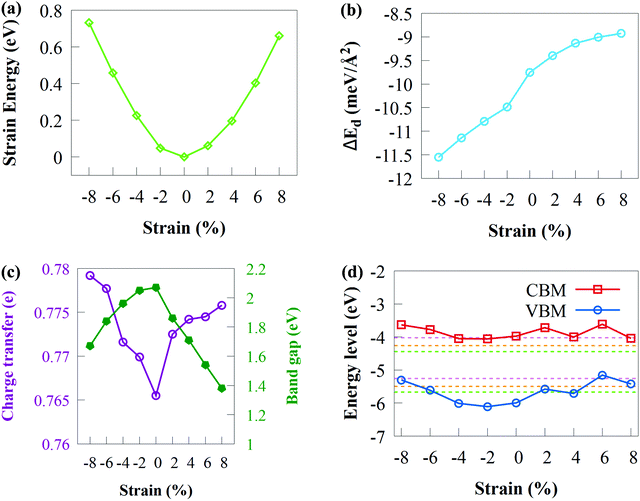
Applying strain is well recognised for its importance in altering the electronic properties of 2D materials80,81 with wide applications in the area of optoelectronic and nanoelectronic devices.82 Various in-plane biaxial strains were induced on the CdS/SiH vdW heterostructure by compressing or stretching the unit cell to gain insight into the effects of mechanical strain on 2D materials. We studied the influence of biaxial strain on the bandgap, band edge position, binding energy and charge transfer of the CdS/SiH vdW heterostructure using a biaxial strain of −8% to +8%. The degree of in-plane biaxial strain is defined according to the following formula: σ = (a − a0)/a0, where a and a0 are the strained and unstrained lattice constants, respectively. We began by investigating the variation in the strain energy of the CdS/SiH vdW heterostructure under biaxial strain and the results are shown in Fig. 8(a).
As shown in Fig. 8(a), the lowest Es was attained when ε = 0. Compressive strain has a slightly larger Es than tensile strain of ε = +8%, showing that compressive strain has a relatively stronger influence on the CdS/SiH vdW heterostructure. Under the applied strains, nearly perfect parabolic curves were formed, suggesting that strain energy is proportional to the square of the strain and elastic strains occur with the applied strain values range from −8 to +8%. Consequently, it can be inferred that the geometrical structure of the CdS/SiH vdW heterostructure remains unchanged under strain deformation, showing that the structure is not disrupted and retains the hexagonal lattice symmetry.
The Eb of the CdS/SiH vdW heterostructure against biaxial strain is shown in Fig. 8(b). Remarkably, Eb increased with an increase in the tensile biaxial strain and decreased with an increase in compressive biaxial strains. The changes in the bandgap energy and charge transfer as a function of biaxial strain are shown in Fig. 8(c). It was observed that the bandgap energy (charge transfer) decreased (increase) when biaxial tensile strain increased. According to Fig. 8(c), it can be observed that the charge transfer increased when the bandgap energy is reduced, indicating that more charge transfers from the CdS monolayer to the SiH monolayer. The bandgap follows the same pattern under compressive strain because more charge transfers at the interface between the CdS and SiH monolayers. Under applied biaxial tensile strain, the bandgap energy of the CdS/SiH vdW heterostructure decreased to 1.38 eV at +8% strain, which is suitable for water splitting. In general, a semiconductor with a narrow bandgap energy requires less energy to transfer electrons from the VB to the CB, which is advantageous for optoelectronic and solar conversion devices.
The band edge of the CdS/SiH vdW heterostructure against biaxial strain is shown in Fig. 8(d). The CBM first moved away and got somewhat close to the water reduction potential in the pH range of 0 to 7 as the biaxial tensile strain increased. In contrast, the VBM moved above the water oxidation potential with applied biaxial tensile strain. This indicates that the oxidising power of the CdS/SiH vdW heterostructure decreased, making it difficult to produce O2. Alternatively, the oxidising power increased when the compressive strain increases up to 4%. When the compressive strain surpassed 4%, the VBM increased over the O2/H2O potential, rendering the heterostructure unsuitable for the OER. The band edges continued to overlap the water reduction potential, showing that the CdS/SiH vdW heterostructure remains a promising photocatalyst for H2 production. Finally, in-plane biaxial stresses significantly altered the band edge positions and photocatalytic activity of the CdS/SiH vdW heterostructure.
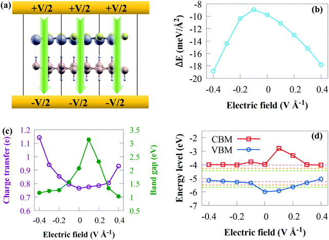
An electric field has the potential to revolutionize chemical synthesis.83 However, no scalable and widely applicable strategies for implementing electric fields have been developed to date.83 Thus, alternative approaches are currently being investigated, most of which exploit the tweezing effect in some way, such as the use of pulsed electric fields in flow-reactors, as well as alternative sources of electric fields, such as laser-induced oscillating fields, plasmonic modes in piezo-electric fields, tribo-electricity, and nanocavities. The use of an external electric field (Efield) has long been recognised as a valuable tool for modifying the electronic and structural properties of 2D materials, which are essential for high-performance electronic devices.84 Consequently, we applied an external Efield in the range of −0.4 to +0.4 V Å−1 to modify the electronic and structural properties of the CdS/SiH vdW heterostructure. Herein, we applied an external Efield and allowed the atoms in the heterostructure to relax. The positive direction is assumed to be from the CdS to SiH monolayer. A schematic model of the application of an external Efield perpendicularly along the z direction of the CdS/SiH vdW heterostructure is shown in Fig. 9(a).
The relative stability may be determined using the binding energy. Fig. 9(b) shows the binding energy of the CdS/SiH vdW heterostructure as a function of Efield. When the applied external Efield fluctuated from −0.4 to +0.4 V Å−1, Ead was always negative, indicating that the CdS/SiH vdW heterostructure always maintains a stable structure. When a positive and negative Efield were applied, Ead decreased rapidly with an increase in Efield.
Fig. 9(c) depicts the evolution of the bandgap as a function of the applied Efield. When the positive Efield of 0 < Efield < +0.2 V Å−1 was applied, the bandgap increased first, which is due to the accelerated transfer of electrons (holes) from the CB (VB) of the CdS (SiH) monolayer to the CB (VB) of the SiH (CdS) monolayer. Then, the bandgap decreased sharply with Efield becoming stronger along the positive direction, and finally became 1.03 eV at the Efield of +0.4 V Å−1. Furthermore, the bandgap energy decreased with Efield of −0.4 V Å−1 < Efield < 0. We observed that the bandgap energy of the CdS/SiH vdW heterostructure is sensitive to the Efield strength.
As illustrated in Fig. 9(c), we plotted the charge transfer versus external Efield. More electrons are transferred as the Efield intensity increases, indicating that interaction between CdS and SiH becomes stronger. It is worth noting that a positive Efield may result in greater charge transfer than a negative Efield. This shows that an external Efield may be used to efficiently tune the charge distribution and carrier concentration, resulting in a change in the band alignment.
To acquire a better understanding of the physical mechanism for the bandgap modified by Efield, we plotted the band edge as a function of the external Efield and water splitting reactions in the pH range of 0 to 7 (see Fig. 9(d)). The charge polarization in the constituent monolayers and the electrostatic potential difference across the interface change when an external Efield is applied.85 Consequently, the band edges contributed by the individual monolayers change with respect to each other, which may alter the relative alignment of the band edges of the heterostructure.85 When Efield varied from −0.1 V Å−1 to −0.4 V Å−1, the positions of both VBM gradually shift upwards, causing the CdS/SiH vdW heterostructure to satisfy the conditions of photocatalytic H2 generation only in the pH range of 0 to 7. Moreover, Efield in the range of +0.2 V Å−1 to +0.4 V Å−1 renders the band edge positions only suitable for photocatalytic H2 generation in the pH range of 0 to 7. Meanwhile, under an Efield of +0.1 V Å−1, the heterostructure may possibly be used for photocatalytic water splitting in the pH range of 0 to 7.
IV. Conclusions
In summary, we systemically studied the stability and optical, electronic and structural properties of the CdS/SiH vdW heterostructure using first-principles hybrid HSE06 functional calculations. The use of the CdS/SiH vdW heterostructure as a visible light photocatalytic water splitting system to create H2 was also investigated. External strain and its effects on the electronic and structural properties of the CdS/SiH vdW heterostructure were also explored. The CdS/SiH vdW heterostructure is energetically stable, as evidenced by the negative binding energy of its four predicted high-symmetry configurations. The computed binding energy (−9.75 meV), phonon dispersions, and AIMD simulations showed that the CdS/SiH vdW heterostructure is stable. CdS and SiH monolayers are direct and indirect semiconductors, with bandgap energies of 2.74 and 2.99 eV, respectively. The vdW interaction between the 2D CdS and SiH monolayers produce a type II heterostructure with an indirect bandgap energy of 2.07 eV bandgap, which allows the efficient spatial separation of charge carriers. The electronic band structures of the CdS and SiH monolayers are not distorted in the CdS/SiH heterostructure due to the weak vdW interactions. Notably, the CdS/SiH vdW heterostructure exhibits a wide optical absorption spectrum with a considerably enhanced absorption intensity in the ultraviolet and visible light regions compared to its isolated monolayers. Furthermore, we discovered that 0.765 electrons moved from CdS to SiH at the CdS/SiH interface, providing a built-in potential in the heterostructure, which effectively prevents the recombination of photogenerated electron–hole pairs and enhances the carrier lifetime. Both the CBM and VBM potentials of the CdS/SiH vdW heterostructure fulfil the criteria of photocatalytic redox potential for water splitting in the pH range of 0 to 7, showing that the CdS/SiH vdW heterostructure may conduct the HER and OER processes successfully. An external electric field and biaxial strain may effectively adjust the electronic band structures and bandgap type of the CdS/SiH vdW heterostructure. Overall, the high optical absorption intensity, effective charge separation, proper bandgap energy and band edge position of CdS/SiH indicate that it can be a potential 2D vdW heterostructure for high-performance visible light water splitting, photoelectric, solar cell, electronic and optoelectronic devices.Conflicts of interest
There are no conflicts to declare.Acknowledgements
The authors are grateful to the Centre for High Performance Computing (CHPC), Cape Town, for the computational resources provided.References
- L. A. Frink and D. W. Armstrong, Anal. Chem., 2016, 88, 8194–8201 CrossRef CAS PubMed.
- P. Chen, F. Dong, M. Ran and J. Li, Chin. J. Catal., 2018, 39, 619–629 CrossRef CAS.
- R. Huang, R. Liang, H. Fan, S. Ying, L. Wu, X. Wang and G. Yan, Sci. Rep., 2017, 7, 1–10 CrossRef PubMed.
- Y. Zhong, Z. He, D. Chen, D. Hao and W. Hao, Appl. Surf. Sci., 2019, 467, 740–748 CrossRef.
- A. Kudo and Y. Miseki, Chem. Soc. Rev., 2009, 38, 253–278 RSC.
- S. Cao, L. Piao and X. Chen, Trends Chem., 2020, 2, 57–70 CrossRef CAS.
- Z. Wang, C. Li and K. Domen, Chem. Soc. Rev., 2019, 48, 2109–2125 RSC.
- T. Hisatomi, J. Kubota and K. Domen, Chem. Soc. Rev., 2014, 43, 7520–7535 RSC.
- R. Gusain, N. Kumar, F. Opoku, P. P. Govender and S. S. Ray, ACS Appl. Nano Mater., 2021, 4, 4721–4734 CrossRef CAS.
- N. Subha, M. Mahalakshmi, M. Myilsamy, B. Neppolian and V. Murugesan, J. Photochem. Photobiol., A, 2019, 379, 150–158 CrossRef CAS.
- X. Zhao, Y. Du, C. Zhang, L. Tian, X. Li, K. Deng, L. Chen, Y. Duan and K. Lv, Chin. J. Catal., 2018, 39, 736–746 CrossRef CAS.
- X. Luo, G. Wang, Y. Huang, B. Wang, H. Yuan and H. Chen, Phys. Chem. Chem. Phys., 2017, 19, 28216–28224 RSC.
- F. Opoku, O. Akoto, S. O.-B. Oppong and A. A. Adimado, New J. Chem., 2021, 45, 20365–20373 RSC.
- F. Opoku, S. O.-B. Oppong, N. K. Asare-Donkor, O. Akoto and A. A. Adimado, Energy Adv., 2022, 1, 146–158 RSC.
- S. Han, Y. Li and Z. Wang, Phys. Chem. Chem. Phys., 2020, 22, 17145–17151 RSC.
- J. Kang, S. Tongay, J. Zhou, J. Li and J. Wu, Appl. Phys. Lett., 2013, 102, 012111 CrossRef.
- I. Roger, M. A. Shipman and M. D. Symes, Nat. Rev. Chem., 2017, 1, 1–13 CrossRef.
- F. Opoku, S. Osei-Bonsu Oppong, A. Aniagyei, O. Akoto and A. A. Adimado, RSC Adv., 2022, 12, 7391–7402 RSC.
- J. Chai, X. Mu, J. Li, L. Zhu, K. Zhai, M. Sun and Y. Li, Spectrochim. Acta, Part A, 2020, 229, 117858 CrossRef CAS PubMed.
- J. Di, J. Xia, H. Li and Z. Liu, Nano Energy, 2017, 35, 79–91 CrossRef CAS.
- B. Luo, G. Liu and L. Wang, Nanoscale, 2016, 8, 6904–6920 RSC.
- Y. Li, Y.-L. Li, B. Sa and R. Ahuja, Catal. Sci. Technol., 2017, 7, 545–559 RSC.
- B. Lalmi, H. Oughaddou, H. Enriquez, A. Kara, S. Vizzini, B. Ealet and B. Aufray, Appl. Phys. Lett., 2010, 97, 223109 CrossRef.
- B. Zeng, Y. Dong, Y. Yi, D. Li, S. Zhang and M. Long, J. Phys.: Condens. Matter, 2019, 31, 165502 CrossRef CAS.
- O. D. Restrepo, R. Mishra, J. E. Goldberger and W. Windl, J. Appl. Phys., 2014, 115, 033711 CrossRef.
- D. Fang, Y. Zhang and S. Zhang, Indones. J. Pharm., 2014, 16, 115006 Search PubMed.
- W. Wei, Y. Dai, B. Huang and T. Jacob, Phys. Chem. Chem. Phys., 2013, 15, 8789–8794 RSC.
- M. Houssa, E. Scalise, K. Sankaran, G. Pourtois, V. Afanas’Ev and A. Stesmans, Appl. Phys. Lett., 2011, 98, 223107 CrossRef.
- J. Zeng, L. Xu, X. Luo, B. Peng, Z. Ma, L.-L. Wang, Y. Yang and C. Shuai, Phys. Chem. Chem. Phys., 2021, 23, 2812–2818 RSC.
- W. Hu, Z. Li and J. Yang, Nano Res., 2017, 10, 2223–2233 CrossRef CAS.
- T. A. Kandiel, I. Ivanova and D. W. Bahnemann, Energy Environ. Sci., 2014, 7, 1420–1425 RSC.
- D. Luo, Y. Huang, Y. Zhao, Y. Fang, Z. Li, Q. Guo, Y. Wei, L. Fan and J. Wu, Int. J. Hydrogen Energy, 2020, 45, 2896–2908 CrossRef CAS.
- Y. Qu, W. Zhou, Y. Xie, L. Jiang, J. Wang, G. Tian, Z. Ren, C. Tian and H. Fu, Chem. Commun., 2013, 49, 8510–8512 RSC.
- S. Ithurria, M. D. Tessier, B. Mahler, R. P.-S. M. Lobo, B. Dubertret and A. L. Efros, Nat. Mater., 2011, 10, 936–941 CrossRef CAS PubMed.
- B. Han, S. Liu, N. Zhang, Y.-J. Xu and Z.-R. Tang, Appl. Catal., B, 2017, 202, 298–304 CrossRef CAS.
- F. Mei, Z. Li, K. Dai, J. Zhang and C. Liang, Chin. J. Catal., 2020, 41, 41–49 CrossRef CAS.
- T. Aramoto, S. Kumazawa, H. Higuchi, T. Arita, S. Shibutani, T. Nishio, J. Nakajima, M. Tsuji, A. Hanafusa and T. Hibino, J. Appl. Phys., 1997, 36, 6304 CrossRef CAS.
- I. Repins, M. A. Contreras, B. Egaas, C. DeHart, J. Scharf, C. L. Perkins, B. To and R. Noufi, Prog. Photovoltaics Res. Appl., 2008, 16, 235–239 CrossRef CAS.
- K. Ramanathan, M. A. Contreras, C. L. Perkins, S. Asher, F. S. Hasoon, J. Keane, D. Young, M. Romero, W. Metzger and R. Noufi, Prog. Photovoltaics Res. Appl., 2003, 11, 225–230 CrossRef CAS.
- A. Medda, A. Dutta, D. Bain, M. K. Mohanta, A. De Sarkar and A. Patra, J. Phys. Chem. C, 2020, 124, 19793–19801 CrossRef CAS.
- L. Cheng, Q. Xiang, Y. Liao and H. Zhang, Energy Environ. Sci., 2018, 11, 1362–1391 RSC.
- P. Vogt, P. De Padova, C. Quaresima, J. Avila, E. Frantzeskakis, M. C. Asensio, A. Resta, B. Ealet and G. Le Lay, Phys. Rev. Lett., 2012, 108, 155501 CrossRef PubMed.
- J. Li and N. Wu, Catal. Sci. Technol., 2015, 5, 1360–1384 RSC.
- L. Xu, Q. Li, X.-F. Li, M.-Q. Long, T. Chen, B. Peng, L.-L. Wang, Y. Yang and C. Shuai, Catal. Sci. Technol., 2019, 9, 3896–3906 RSC.
- J. Low, J. Yu, M. Jaroniec, S. Wageh and A. A. Al-Ghamdi, Adv. Mater., 2017, 29, 1601694 CrossRef.
- R. Ahammed, A. Rawat, N. Jena, M. K. Mohanta and A. De Sarkar, Appl. Surf. Sci., 2020, 499, 143894 CrossRef CAS.
- J. Chen, X. Wei, R. Zhang, J. Liu, Y. Tian, Y. Zhang, T. Guo, J. Fan, L. Ni and M. Zhang, Adv. Mater. Interfaces, 2021, 8, 2002068 CrossRef CAS.
- Y. Guo, J. Min, X. Cai, L. Zhang, C. Liu and Y. Jia, J. Phys. Chem. C, 2022, 126, 4677–4683 CrossRef CAS.
- A. Rawat, R. Ahammed, S. Dimple, N. Jena, M. K. Mohanta and A. De Sarkar, J. Phys. Chem. C, 2019, 123, 12666–12675 CrossRef CAS.
- J. Ren, C. Zhang, C. He, T. Ouyang, J. Li, C. Tang and J. Zhong, J. Appl. Phys., 2020, 128, 043103 CrossRef CAS.
- Z. Cui, K. Ren, Y. Zhao, X. Wang, H. Shu, J. Yu, W. Tang and M. Sun, Appl. Surf. Sci., 2019, 492, 513–519 CrossRef CAS.
- K. Ren, M. Sun, Y. Luo, S. Wang, J. Yu and W. Tang, Appl. Surf. Sci., 2019, 476, 70–75 CrossRef CAS.
- X. Zhang, A. Chen, Z. Zhang, M. Jiao and Z. Zhou, Nanoscale Adv., 2019, 1, 154–161 RSC.
- T. Su, Q. Shao, Z. Qin, Z. Guo and Z. Wu, ACS Catal., 2018, 8, 2253–2276 CrossRef CAS.
- M. Niu, D. Cheng and D. Cao, Sci. Rep., 2014, 4, 1–6 Search PubMed.
- S. Han, Y. Li, J. Chai and Z. Wang, Phys. Chem. Chem. Phys., 2020, 22, 8565–8571 RSC.
- W. Sheng, Y. Xu, M. Liu, G. Nie, J. Wang and S. Gong, Phys. Chem. Chem. Phys., 2020, 22, 21436–21444 RSC.
- M. K. Mohanta and A. D. Sarkar, ACS Appl. Mater. Interfaces, 2020, 12, 18123–18137 CrossRef CAS PubMed.
- A. Jana, C. Bhattacharya and J. Datta, Electrochim. Acta, 2010, 55, 6553–6562 CrossRef CAS.
- P. Giannozzi, O. Andreussi, T. Brumme, O. Bunau, M. Buongiorno Nardelli, M. Calandra, R. Car, C. Cavazzoni, D. Ceresoli, M. Cococcioni, N. Colonna, I. Carnimeo, A. Dal Corso, S. de Gironcoli, P. Delugas, R. A. DiStasio, A. Ferretti, A. Floris, G. Fratesi, G. Fugallo, R. Gebauer, U. Gerstmann, F. Giustino, T. Gorni, J. Jia, M. Kawamura, H. Y. Ko, A. Kokalj, E. Küçükbenli, M. Lazzeri, M. Marsili, N. Marzari, F. Mauri, N. L. Nguyen, H. V. Nguyen, A. Otero-de-la-Roza, L. Paulatto, S. Poncé, D. Rocca, R. Sabatini, B. Santra, M. Schlipf, A. P. Seitsonen, A. Smogunov, I. Timrov, T. Thonhauser, P. Umari, N. Vast, X. Wu and S. Baroni, J. Phys.: Condens. Matter, 2017, 29, 465901 CrossRef CAS PubMed.
- D. Hamann, Phys. Rev. B: Condens. Matter Mater. Phys., 2013, 88, 085117 CrossRef.
- J. P. Perdew, K. Burke and M. Ernzerhof, Phys. Rev. Lett., 1996, 77, 3865–3868 CrossRef CAS PubMed.
- S. Grimme, J. Antony, S. Ehrlich and H. Krieg, J. Chem. Phys., 2010, 132, 154104 CrossRef PubMed.
- S. Grimme, S. Ehrlich and L. Goerigk, J. Comput. Chem., 2011, 32, 1456–1465 CrossRef CAS PubMed.
- H. J. Monkhorst and J. D. Pack, Phys. Rev. B: Condens. Matter Mater. Phys., 1976, 13, 5188–5192 CrossRef.
- J. Heyd, G. E. Scuseria and M. Ernzerhof, J. Chem. Phys., 2003, 118, 8207–8215 CrossRef CAS.
- L. Bengtsson, Phys. Rev. B: Condens. Matter Mater. Phys., 1999, 59, 12301 CrossRef CAS.
- D. Sanchez-Portal, E. Artacho and J. M. Soler, Solid State Commun., 1995, 95, 685–690 CrossRef CAS.
- S. Baroni, S. De Gironcoli, A. Dal Corso and P. Giannozzi, Rev. Mod. Phys., 2001, 73, 515 CrossRef CAS.
- G. J. Martyna, M. L. Klein and M. Tuckerman, J. Chem. Phys., 1992, 97, 2635–2643 CrossRef.
- K. Zheng, Q. Yang, C. J. Tan, H. Y. Ye and X. P. Chen, Phys. Chem. Chem. Phys., 2017, 19, 18330–18337 RSC.
- Z.-K. Tang, Y.-N. Zhang, D.-Y. Zhang, W.-M. Lau and L.-M. Liu, Sci. Rep., 2014, 4, 1–7 Search PubMed.
- M. K. Mohanta, A. Rawat, N. Jena, R. Ahammed and A. De Sarkar, J. Phys.: Condens. Matter, 2020, 32, 355301 CrossRef CAS PubMed.
- A. D. Becke and K. E. Edgecombe, J. Chem. Phys., 1990, 92, 5397–5403 CrossRef CAS.
- J. Liu and E. Hua, Mater. Sci. Semicond. Process., 2015, 40, 446–452 CrossRef CAS.
- Q. Wu, W. Wei, F. Li, B. Huang and Y. Dai, J. Phys. D: Appl. Phys., 2019, 52, 335303 CrossRef CAS.
- O. B. Malcıoğlu, R. Gebauer, D. Rocca and S. Baroni, Comput. Phys. Commun., 2011, 182, 1744–1754 CrossRef.
- X. Ge, S. J. Binnie, D. Rocca, R. Gebauer and S. Baroni, Comput. Phys. Commun., 2014, 185, 2080–2089 CrossRef CAS.
- Y. Gai, J. Li, S.-S. Li, J.-B. Xia and S.-H. Wei, Phys. Rev. Lett., 2009, 102, 036402 CrossRef PubMed.
- Y. Chen, Q. Sun and P. Jena, J. Mater. Chem. C, 2016, 4, 6353–6361 RSC.
- X. Qian, L. Fu and J. Li, Nano Res., 2015, 8, 967–979 CrossRef CAS.
- J. Li, Z. Shan and E. Ma, MRS Bull., 2014, 39, 108–114 CrossRef CAS.
- S. Shaik, D. Danovich, J. Joy, Z. Wang and T. Stuyver, J. Am. Chem. Soc., 2020, 142, 12551–12562 CrossRef CAS PubMed.
- B. Zhou, X. Wang, S. Dong, K. Zhang and W. Mi, Carbon, 2017, 120, 121–127 CrossRef CAS.
- M. K. Mohanta and A. De Sarkar, Nanoscale, 2020, 12, 22645–22657 RSC.
| This journal is © The Royal Society of Chemistry 2022 |

