 Open Access Article
A heterogeneous reaction strategy towards the general synthesis of 2D non-layered nanomaterials†
Wenjing
Qin‡
,
Hao
Liu‡
,
Jiahui
Liu
,
Jiangbo
Yuan
,
Cong
Wei
 * and
Qun
Xu
 *
*
College of Materials Science and Engineering, Zhengzhou University, Zhengzhou, 450001, China. E-mail: weicong@zzu.edu.cn; qunxu@zzu.edu.cn
First published on 10th May 2022
Abstract
2D non-layered materials exhibit various exotic physical and chemical features that are distinctly different from their layered counterparts, but a general synthesis approach is still lacking for their intrinsic isotropic chemical bonds. In this study, a diffusion-controlled heterogeneous interfacial reaction strategy was proposed to drive the 2D anisotropic growth of the non-layered crystals. 2–3 nm thick single-crystalline hexagonal CdS nanosheets were obtained via a facile gas–liquid reaction. The diffusion of the Cd and S precursors was impeded by the interphase boundary and only the ultrathin interfacial region had sufficient reactants to afford the chemical conversion, leading to the naturally confined 2D anisotropic growth of the CdS crystals. Besides, this universal approach can be easily extended to synthesize other 2D non-layered materials, and various ultra-thin non-layered nanosheets, such as orthorhombic Bi2S3, monoclinic CuO, anatase TiO2 and cubic Al2O3, have been successfully obtained by designing appropriate heterogeneous reaction systems. Our results provide a robust access to the 2D non-layered materials that may lead to a significant proliferation of the 2D family.
The ultrathin planar structure endows two-dimensional (2D) materials with extremely high surface percentage, extraordinary physical strength, superior flexibility, tunable optoelectronic performance and excellent catalytic properties,1–4 providing a wealth of potential applications in both academic and industrial communities.5 Nonetheless, the obtained 2D materials are largely limited to the layered compounds, which can be easily produced via mechanical exfoliation,6 liquid exfoliation,7 ion intercalation,8 chemical vapor deposition,9,10etc. For their non-layered counterparts, these traditional approaches are always not applicable. Creating atomically thin nanosheets from non-layered materials is expected to enrich the portfolio of 2D materials11 and bring out exotic properties due to their abundant surface dangling bonds, massively coordinated-unsaturated surface atoms and clear structural distortion that are absent in the case of 2D layered ones.12–14 However, the intrinsic three-dimensional chemically bonded lattices of the non-layered compounds lack the driving force for the 2D anisotropic growth,15 posing a formidable challenge for the preparation of 2D non-layered materials.
Currently available strategies are mostly based on the wet chemical synthesis (e.g., self-assembly,16,17 oriented attachment,18,19 lamellar intermediate-assisted exfoliation20–22 and topochemical transformation23–26), typically using soft or hard templates to direct the anisotropic growth of the non-layered crystals.27–30 However, these methods always require very stringent experimental conditions and can hardly be extended to synthesize other 2D non-layered materials.12,31 In heterogeneous reactions, such as the gas–liquid and solid–solid reactions, the mass diffusion process is always severely suppressed and the chemical conversion primarily occurs at the interface of the involved reactants.32–34 Only the very top surface of the reactants can convert into the products at the initial stage and this atomically thin interfacial product is considered naturally formed 2D structure,35 which would in principle provide a universal and robust strategy for the synthesis of 2D non-layered materials.
In this study, we have developed a heterogeneous reaction strategy for the general synthesis of 2D non-layered materials. For example, ultrathin hexagonal CdS nanosheets (non-layered crystal lattice, PDF# 41-1049) with a thickness of about 2.7 nm and lateral dimensions of up to 300 nm were successfully obtained via a gas–liquid reaction. The gas–liquid interphase boundary set a natural diffusion barrier for the reactants; thus, the encounter of the involved precursors was mainly limited near the interface region, driving the 2D anisotropic growth of the products. Moreover, our strategy exhibits remarkable generality and various 2D non-layered nanomaterials, including orthorhombic Bi2S3 (PDF# 17-0320), monoclinic CuO (PDF# 45-0937), anatase TiO2 (PDF# 21-1272) and cubic Al2O3 (PDF# 29-0063), have been successfully synthesized via other heterogeneous reactions (e.g., solid–solid and solid–liquid–solid reactions). We anticipate that our results would provide profitable enlightenment for the fabrication of 2D non-layered nanoarchitecture, which would greatly enlarge the family of 2D materials.
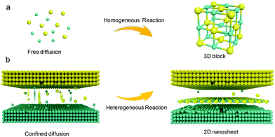
The synthesis strategy is illustrated in Scheme 1. In a homogeneous reaction system, all the involved precursors are well mixed and can migrate freely. The morphology of the product is mainly determined by the surface lattice energy. Crystal growth rates in the direction perpendicular to a high-index plane with high surface energy are usually much faster than those along the normal direction of a low-index plane, so high-index planes are rapidly eliminated, generally forming three-dimensional block structures.36–38 In contrast, for the heterogeneous system, the reactants are present in different phases. The interphase boundary severely impedes the diffusion and migration of the reactants.33 The collision and transformation of the involved precursors are predominantly confined to the interface,39 providing a driving force for the 2D anisotropic growth of the products.
2D non-layered CdS nanosheets, synthesized via a gas–liquid reaction, were chosen as an example. In a routine process, 5 mg thiourea solid particles were first dissolved in alcohol and recrystallized in the bottom of an autoclave. Moreover, 5 mg CdCl2 powder was dissolved in 1 mL PEG200. A homemade apparatus was built to spatially separate the Cd and S precursors (Fig. S1, ESI†). The reactor was sealed and thermally treated for 1 h at 180 °C, which is above the vaporization temperature of thiourea (Fig. S2, ESI†). The vaporized S precursor diffused and encountered the Cd ions at the gas–liquid interface. Further diffusion was impeded by the interphase boundary and only the ultrathin interface region had sufficient S precursors to support the sulfuration reaction, leading to the confined 2D anisotropic growth of the CdS crystals. Excess organics and remnant salt were removed by washing with water. Dispersed nanosheets were obtained via an ultrasonic treatment and used for the detailed structural characterization.
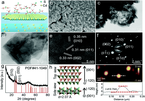
The 2D morphology of the obtained CdS crystals was confirmed by scanning electron microscopy (SEM) and transmission electron microscopy (TEM). As shown in Fig. 1b–d, the obtained CdS nanosheets have thin thicknesses with lateral dimensions ranging from 200 to 300 nm. CdS nanosheets tend to stack with each other for their high surface energy (Fig. 1b and c), which is similar to the general behavior of graphene-like structures.40 As shown in the high-resolution TEM image (Fig. 1e), clear lattice fringes with interplanar distances of 0.31, 0.33 and 0.35 nm are observed. The selected area electron diffraction (SAED) patterns show pseudo-six-fold symmetry diffraction spots (Fig. 1f), indicating that the obtained CdS nanosheets are single-crystal structures. As shown in Fig. 1g, the diffraction peaks in the X-ray diffraction (XRD) profile correspond well to the hexagonal structure of CdS (PDF# 41-1049), with a = 4.14 Å, b = 4.14 Å and c = 6.71 Å. The lattice fringes of 0.31, 0.33 and 0.35 nm and can be indexed to the (0 1 1), (0 0 2) and (0 1 0) planes of the hexagonal CdS, respectively, in accordance with the SAED patterns. These results elucidate that the as-prepared nanosheets correspond to the (−1 2 0) plane of hexagonal CdS. In comparison with its bulk counterpart (Fig. S3, ESI†), the peak intensity at 43.7°, corresponding to the reflection of the (−1 2 0) plane, significantly decreases in the XRD profile of the CdS nanosheets, further verifying the 2D planar character of the obtained sample. Fig. 1h displays the crystal structure of the 2D CdS nanosheets. The Cd atoms are coordinated by four O atoms to form two types of tetrahedrons and the tetrahedrons are connected to each other by corners, exhibiting a typical non-layered crystal lattice. According to the atomic force microscope (AFM) measurements, the obtained 2D CdS nanosheets have an average thickness of about 2.7 nm (Fig. 1i and Fig. S4, ESI†), which is only equivalent to 13 unit cells with a single layer of 2.07 Å.
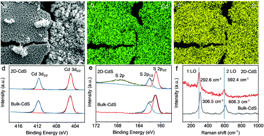
Energy-dispersive X-ray spectroscopy (EDS) was employed to further identify the composition. The elemental mapping images (Fig. 2a–c and Fig. S6, ESI†) demonstrate the uniform distribution of Cd and S elements in the as-synthesized nanosheets. The EDS spectrum in Fig. S6 (ESI†) shows an atomic ratio (Cd![[thin space (1/6-em)]](https://www.rsc.org/images/entities/char_2009.gif) :
:![[thin space (1/6-em)]](https://www.rsc.org/images/entities/char_2009.gif) S) of 0.52
S) of 0.52![[thin space (1/6-em)]](https://www.rsc.org/images/entities/char_2009.gif) :
:![[thin space (1/6-em)]](https://www.rsc.org/images/entities/char_2009.gif) 0.48, very close to 1
0.48, very close to 1![[thin space (1/6-em)]](https://www.rsc.org/images/entities/char_2009.gif) :
:![[thin space (1/6-em)]](https://www.rsc.org/images/entities/char_2009.gif) 1, in agreement with the stoichiometric ratio of the CdS crystal. The surface elemental compositions and surface chemical states of the as-prepared CdS nanosheets were further investigated by X-ray photoelectron spectroscopy (XPS). As shown in the high-resolution XPS spectrum of Cd 3d (Fig. 2d), there are two strong peaks at 404.9 and 411.7 eV in the CdS nanosheets, corresponding to the 3d5/2 and 3d3/2 orbital electrons of Cd2+ states. No additional satellite peaks are observed near the Cd2+ 3d3/2 and Cd2+ 3d5/2 peaks, which is well consistent with the structure of bulk CdS crystals,41 indicating that the Cd ion in the obtained 2D CdS sheets has a high chemical purity without other valence states.
1, in agreement with the stoichiometric ratio of the CdS crystal. The surface elemental compositions and surface chemical states of the as-prepared CdS nanosheets were further investigated by X-ray photoelectron spectroscopy (XPS). As shown in the high-resolution XPS spectrum of Cd 3d (Fig. 2d), there are two strong peaks at 404.9 and 411.7 eV in the CdS nanosheets, corresponding to the 3d5/2 and 3d3/2 orbital electrons of Cd2+ states. No additional satellite peaks are observed near the Cd2+ 3d3/2 and Cd2+ 3d5/2 peaks, which is well consistent with the structure of bulk CdS crystals,41 indicating that the Cd ion in the obtained 2D CdS sheets has a high chemical purity without other valence states.
For the S element, the binding energies of the S 2p1/2 and S 2p3/2 states at 162.0 eV and 160.8 eV, respectively, are clearly observed in the S 2p core spectrum (Fig. 2e). However, a broad additional peak located at 167.5 eV emerges in the spectrum of 2D CdS sheets that is absent in the spectrum of the bulk sample. The new peak might be related to the abundant surface dangling bonds of the 2D non-layered CdS nanosheets, which would act as the chemical adsorption sites for the oxygen species to form new S–O bonds that can increase the electron binding energy of S 2p.42 As shown in Fig. 2f, the corresponding Raman spectroscopy studies indicate that the as-prepared 2D nanosheets exhibit Raman scattering peaks at 294 and 595 cm−1, which correspond to the 1 LO and 2 LO vibration modes of CdS.43 The clear red shift (14 cm−1) and broadening of the 1 LO and 2 LO peaks are clearly observed due to the attenuation of the Cd–S bond oscillator strength induced by the abundant surface dangling bonds,44 further confirming the 2D non-layered structure of the as-prepared CdS.
To investigate the formation mechanism of the CdS nanosheets, products were collected and characterized at different time points. The corresponding SEM images in Fig. 3a–c and the conceptual drawing shown below the images (Fig. 3d) illustrate the structure evolution of the nanosheets. In the initial period, only discrete particles appeared at the gas–liquid interface (Fig. 3a), which could act as the nucleating agents for the subsequent precursors. As the precursor diffusion was severely impeded by the interphase boundary, the particles mainly grew laterally along with the gas–liquid interface, forming an amorphous 2D structure (Fig. 3b). The liquid level can be easily perturbed by the external airflow and the internal thermal-convection; thus, the formed 2D nanosheets would inevitably collide and gradually stack with each other due to their high surface energy. With the increase in the thermal treatment time, the stacked 2D amorphous sheets were fully crystallized and became crystalline nanosheets eventually (Fig. 3c). The role of the gas–liquid heterogeneous reaction in the formation of the 2D nanosheets was investigated by performing the synthesis in a homogeneous reaction system. Fig. S7 (ESI†) presents the morphology of the synthesized CdS via a normal solvothermal reaction, in which Cd ions and thiourea were well mixed and homogeneously dispersed. Clear rod-like rather than 2D-shaped crystals were obtained, confirming that the heterogeneous reaction system was the key point for the formation of the 2D CdS nanosheets.
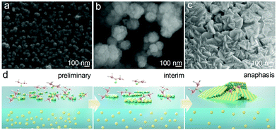 | ||
| Fig. 3 SEM images of the CdS nanosheets obtained at different growth times: (a) 15 min; (b) 30 min; (c) 1 h. (d) Schematic illustration of the growth process of the CdS nanosheets. | ||
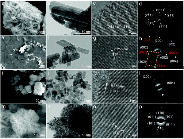
To demonstrate the generality of our strategy, some other typical heterogeneous reaction systems, such as solid–solid and solid–liquid–solid reactions, were applied to synthesize the 2D non-layered nanomaterials, including orthorhombic Bi2S3, monoclinic CuO, anatase TiO2 and cubic Al2O3. Details of the synthetic recipes and reaction conditions for the individual samples can be found in the ESI.† We performed the SEM and TEM analyses on the as-synthesized 2D non-layered nanosheets. The 2D features of Bi2S3, CuO, TiO2 and Al2O3 can be clearly identified in the SEM images (Fig. 4a, e, i and m) and TEM images (Fig. 4b, f, j and n). The lateral sizes and thicknesses of the nanosheets vary with the chemical composition: 50–200 nm and 6.9 nm for Bi2S3, 150 nm and 5.3 nm for CuO, 50 nm and 2.8 nm for TiO2, 200 nm and 1.1 nm for Al2O3 (Fig. S8, ESI†). Due to the intrinsic high lattice strain in 2D non-layered structures, clear dissociation defects can be observed in the TiO2 nanosheets (Fig. 4j and k) and the ultrathin Al2O3 nanosheets even spontaneously folded into the wrinkled nanoflowers (Fig. 4m and n).
In addition, all the synthesized nanosheets are well crystallized. Clear lattice fringes and regular diffraction spots are presented in their HRTEM images (Fig. 4c, g, k and o) and SAED patterns (Fig. 4d, h, l and p). Fig. S9 (ESI†) displays their corresponding XRD patterns, demonstrating that the Bi2S3, CuO, TiO2 and Al2O3 nanosheets reserved well-crystallized orthorhombic (PDF# 17-0320), monoclinic (PDF# 45-0937), anatase (PDF# 21-1272) and cubic (PDF# 29-0063) non-layered phases, respectively. The intrinsic non-layered structure endows them with numerous dangling bonds and massive coordinated-unsaturated atoms on their surfaces that can enhance the chemical adsorption capacity for the ambient molecules, especially the ubiquitous oxygen species.45 This phenomenon was confirmed from the XPS results of these nanosheets, which exhibit additional peaks corresponding to the hydroxide or S–O bonding (Fig. S10, ESI†).46,47 Moreover, their Raman spectra also show a distinct red shift compared with their bulk counterparts (Fig. S11, ESI†), suggesting obvious lattice relaxation in the 2D non-layered structures.48 The typical 2D non-layered features that existed in the obtained nanosheets demonstrate the generality of the heterogeneous reaction strategy and indicate its feasibility to be extended to the synthesis of other 2D non-layered nanostructures.
In summary, we have developed a facile and general route to produce various 2D non-layered nanosheets via heterogeneous reaction methods (including gas–liquid, solid–solid and solid–liquid–solid reactions). This approach was exemplified by fabricating the crystalized 2D ultrathin nanosheets of metal sulfides (e.g., Bi2S3, CdS) and metal oxides (e.g., CuO, TiO2, Al2O3), none of which possess an original layered structure in their bulk crystals. By designing an appropriate heterogeneous reaction system and adjusting target precursors, the approach should be possible to largely extend to obtain other 2D non-layered nanosheets. We hope this synthetic principle will provide more experience and efficiency in the fabrication of 2D non-layered nanomaterials so that more practical applications of 2D non-layered materials can be explored.
Conflicts of interest
There are no conflicts to declare.Acknowledgements
This work was supported by the National Natural Science Foundation of China (No. 21805246, 22175154, 21773216, 51173170), the joint project from the Henan-Provincial and the China-National Natural Science Foundations (Project No. U2004208).Notes and references
- D. Akinwande, C. Huyghebaert, C.-H. Wang, M. I. Serna, S. Goossens, L.-J. Li, H. S.-P. Wong and F. H.-L. Koppens, Nature, 2019, 573, 507–518 CrossRef CAS PubMed.
- A. Rodin, M. Trushin, A. Carvalho and A. H. Castro Neto, Nat. Rev. Phys., 2020, 2, 524–537 CrossRef.
- C. Tan, X. Cao, X.-J. Wu, Q. He, J. Yang, X. Zhang, J. Chen, W. Zhao, S. Han, G.-H. Nam, M. Sindoro and H. Zhang, Chem. Rev., 2017, 117, 6225–6331 CrossRef CAS PubMed.
- F. Wang, P. Luo, Y. Zhang, Y. Huang, Q. Zhang, Y. Li and T. Zhai, Sci. China Mater., 2020, 63, 1537–1547 CrossRef CAS.
- C. Jiang, H. Li and C. Wang, Sci. Bull., 2017, 62, 1473–1490 CrossRef CAS.
- Y. Huang, Y.-H. Pan, R. Yang, L.-H. Bao, L. Meng, H.-L. Luo, Y.-Q. Cai, G.-D. Liu, W.-J. Zhao, Z. Zhou, L.-M. Wu, Z.-L. Zhu, M. Huang, L.-W. Liu, L. Liu, P. Cheng, K.-H. Wu, S.-B. Tian, C.-Z. Gu, Y.-G. Shi, Y.-F. Guo, Z. G. Cheng, J.-P. Hu, L. Zhao, G.-H. Yang, E. Sutter, P. Sutter, Y.-L. Wang, W. Ji, X.-J. Zhou and H.-J. Gao, Nat. Commun., 2020, 11, 2453 CrossRef CAS PubMed.
- S. Witomska, T. Leydecker, A. Ciesielski and P. Samorì, Adv. Funct. Mater., 2019, 29, 1901126 CrossRef.
- M. S. Stark, K. L. Kuntz, S. J. Martens and S. C. Warren, Adv. Mater., 2019, 31, 1808213 CrossRef PubMed.
- J. Zhou, J. Lin, X. Huang, Y. Zhou, Y. Chen, J. Xia, H. Wang, Y. Xie, H. Yu, J. Lei, D. Wu, F. Liu, Q. Fu, Q. Zeng, C.-H. Hsu, C. Yang, L. Lu, T. Yu, Z. Shen, H. Lin, B. I. Yakobson, Q. Liu, K. Suenaga, G. Liu and Z. Liu, Nature, 2018, 556, 355–359 CrossRef CAS PubMed.
- K. Liu, B. Jin, W. Han, X. Chen, P. Gong, L. Huang, Y. Zhao, L. Li, S. Yang, X. Hu, J. Duan, L. Liu, F. Wang, F. Zhuge and T. Zhai, Nat. Electron., 2021, 4, 906–913 CrossRef CAS.
- S. Liu, L. Xie, H. Qian, G. Liu, H. Zhong and H. Zeng, J. Mater. Chem. A, 2019, 7, 15411–15419 RSC.
- Y. Dou, L. Zhang, X. Xu, Z. Sun, T. Liao and S. X. Dou, Chem. Soc. Rev., 2017, 46, 7338–7373 RSC.
- Y. Wang, Z. Zhang, Y. Mao and X. Wang, Energy Environ. Sci., 2020, 13, 3993–4016 RSC.
- J. Peng, Y. Liu, H. Lv, Y. Li, Y. Lin, Y. Su, J. Wu, H. Liu, Y. Guo, Z. Zhuo, X. Wu, C. Wu and Y. Xie, Nat. Chem., 2021, 13, 1235–1240 CrossRef CAS PubMed.
- Y. Chen, Z. Fan, Z. Zhang, W. Niu, C. Li, N. Yang, B. Chen and H. Zhang, Chem. Rev., 2018, 118, 6409–6455 CrossRef CAS PubMed.
- S. Gao, Y. Lin, X. Jiao, Y. Sun, Q. Luo, W. Zhang, D. Li, J. Yang and Y. Xie, Nature, 2016, 529, 68–71 CrossRef CAS PubMed.
- H. Duan, N. Yan, R. Yu, C.-R. Chang, G. Zhou, H.-S. Hu, H. Rong, Z. Niu, J. Mao, H. Asakura, T. Tanaka, P. J. Dyson, J. Li and Y. Li, Nat. Commun., 2014, 5, 3093 CrossRef PubMed.
- F. Wang, J.-H. Seo, G. Luo, M. B. Starr, Z. Li, D. Geng, X. Yin, S. Wang, D. G. Fraser, D. Morgan, Z. Ma and X. Wang, Nat. Commun., 2016, 7, 10444 CrossRef CAS PubMed.
- M. P. Boneschanscher, W. H. Evers, J. J. Geuchies, T. Altantzis, B. Goris, F. T. Rabouw, S. A.-P. V. Rossum, H. S.-J. V.-D. Zant, L. D.-A. Siebbeles, G. V. Tendeloo, I. Swart, J. Hilhorst, A. V. Petukhov, S. Bals and D. Vanmaekelbergh, Science, 2014, 344, 1377–1380 CrossRef CAS PubMed.
- Y. Sun, Z. Sun, S. Gao, H. Cheng, Q. Liu, J. Piao, T. Yao, C. Wu, S. Hu, S. Wei and Y. Xie, Nat. Commun., 2012, 3, 1057 CrossRef PubMed.
- Z. Sun, T. Liao, Y. Dou, S. M. Hwang, M.-S. Park, L. Jiang, J. H. Kim and S. X. Dou, Nat. Commun., 2014, 5, 3813 CrossRef CAS PubMed.
- Y. Du, Z. Yin, J. Zhu, X. Huang, X.-J. Wu, Z. Zeng, Q. Yan and H. Zhang, Nat. Commun., 2012, 3, 1177 CrossRef PubMed.
- L. Kubie, M. S. Martinez, E. M. Miller, L. M. Wheeler and M. C. Beard, J. Am. Chem. Soc., 2019, 141, 12121–12127 CrossRef CAS PubMed.
- S. Yang, G. Chen, A. G. Ricciardulli, P. Zhang, Z. Zhang, H. Shi, J. Ma, J. Zhang, P. W.-M. Blom and X. Feng, Angew. Chem., Int. Ed., 2020, 59, 465–470 CrossRef CAS PubMed.
- L. Najafi, R. Oropesa-Nuñez, S. Bellani, B. Martín-García, L. Pasquale, M. Serri, F. Drago, J. Luxa, Z. Sofer, D. Sedmidubský, R. Brescia, S. Lauciello, M. I. Zappia, D. V. Shinde, L. Manna and F. Bonaccorso, ACS Nano, 2022, 16, 351–367 CrossRef CAS PubMed.
- P. Liu, P. M. Abdala, G. Goubert, M.-G. Willinger and C. Copéret, Angew. Chem., Int. Ed., 2021, 60, 3254–3260 CrossRef CAS PubMed.
- H. Zhao, Y. Zhu, F. Li, R. Hao, S. Wang and L. Guo, Angew. Chem., Int. Ed., 2017, 56, 8766–8770 CrossRef CAS PubMed.
- C. Gong, J. Chu, C. Yin, C. Yan, X. Hu, S. Qian, Y. Hu, K. Hu, J. Huang, H. Wang, Y. Wang, P. Wangyang, T. Lei, L. Dai, C. Wu, B. Chen, C. Li, M. Liao, T. Zhai and J. Xiong, Adv. Mater., 2019, 31, 1903580 CrossRef PubMed.
- C. Zhao, H. Zhang, W. Si and H. Wu, Nat. Commun., 2016, 7, 12543 CrossRef CAS PubMed.
- D. Wang, W. Zhou, R. Zhang, J. Zeng, Y. Du, S. Qi, C. Cong, C. Ding, X. Huang, G. Wen and T. Yu, Adv. Mater., 2018, 30, 1803569 CrossRef PubMed.
- F. Wang, Z. Wang, T. A. Shifa, Y. Wen, F. Wang, X. Zhan, Q. Wang, K. Xu, Y. Huang, L. Yin, C. Jiang and J. He, Adv. Funct. Mater., 2017, 27, 1603254 CrossRef.
- A. Zavabeti, J. Z. Ou, B. J. Carey, N. Syed, R. Orrell-Trigg, E. L.-H. Mayes, C. Xu, O. Kavehei, A. P. O’Mullane, R. B. Kaner, K. Kalantar-zadeh and T. Daeneke, Science, 2017, 358, 332–335 CrossRef CAS PubMed.
- B. Y. Zhang, K. Xu, Q. Yao, A. Jannat, G. Ren, M. R. Field, X. Wen, C. Zhou, A. Zavabeti and J. Z. Ou, Nat. Mater., 2021, 20, 1073–1078 CrossRef CAS PubMed.
- X. Lin, P. Yan, F. Xu, W. Wu, T. Hu, C. Wei and Q. Xu, J. Mater. Chem. C, 2019, 7, 7196–7200 RSC.
- N. Syed, A. Zavabeti, K. A. Messalea, E. Della Gaspera, A. Elbourne, A. Jannat, M. Mohiuddin, B. Y. Zhang, G. Zheng, L. Wang, S. P. Russo, D. Esrafilzadeh, C. F. McConville, K. Kalantar-Zadeh and T. Daeneke, J. Am. Chem. Soc., 2019, 141, 104–108 CrossRef CAS PubMed.
- Q. Chen, Y. Jia, S. Xie and Z. Xie, Chem. Soc. Rev., 2016, 45, 3207–3220 RSC.
- N. Tian, Z.-Y. Zhou, S.-G. Sun, Y. Ding and Z. L. Wang, Science, 2007, 316, 732–735 CrossRef CAS PubMed.
- G. Liu, H. G. Yang, J. Pan, Y. Q. Yang, G. Q. Lu and H.-M. Cheng, Chem. Rev., 2014, 114, 9559–9612 CrossRef CAS PubMed.
- C. Gadiyar, A. Loiudice, F. D’Ambra, E. Oveisi, D. Stoian, P. Iyengar, L. Castilla-Amorós, V. Mantella and R. Buonsanti, J. Am. Chem. Soc., 2020, 142, 15931–15940 CrossRef CAS PubMed.
- Q. Pan, F. Zheng, Y. Wu, X. Ou, C. Yang, X. Xiong and M. Liu, J. Mater. Chem. A, 2018, 6, 592–598 RSC.
- M. Chen, Y. N. Kim, C. Li and S. O. Cho, Cryst. Growth Des., 2008, 8, 629–634 CrossRef CAS.
- Z. Zhao-Karger, X. Zhao, D. Wang, T. Diemant, R. J. Behm and M. Fichtner, Adv. Energy Mater., 2015, 5, 1401155 CrossRef.
- B. Jin, P. Huang, Q. Zhang, X. Zhou, X. Zhang, L. Li, J. Su, H. Li and T. Zhai, Adv. Funct. Mater., 2018, 28, 1800181 CrossRef.
- C. Hu, X. Zeng, J. Cui, H. Chen and J. Lu, J. Phys. Chem. C, 2013, 117, 20998–21005 CrossRef CAS.
- H. Wu, X. Lu, G. Zheng and G. W. Ho, Adv. Energy Mater., 2018, 8, 1702704 CrossRef.
- J. Gu, C. Zhang, Z. Du and S. Yang, Small, 2019, 15, 1904587 CrossRef CAS PubMed.
- M. B. Ghasemian, M. Mayyas, S. A. Idrus-Saidi, M. A. Jamal, J. Yang, S. S. Mofarah, E. Adabifiroozjaei, J. Tang, N. Syed, A. P. O'Mullane, T. Daeneke and K. Kalantar-Zadeh, Adv. Funct. Mater., 2019, 29, 1901649 CrossRef.
- S. Zhou, R. Wang, J. Han, D. Wang, H. Li, L. Gan and T. Zhai, Adv. Funct. Mater., 2019, 29, 1805880 CrossRef.
Footnotes |
| † Electronic supplementary information (ESI) available: Detailed synthesis procedure and additional figures (Fig. S1–S9). See DOI: https://doi.org/10.1039/d2ma00412g |
| ‡ These authors contributed equally to this work. |
| This journal is © The Royal Society of Chemistry 2022 |

