DOI:
10.1039/D2MA00738J
(Paper)
Mater. Adv., 2022,
3, 8740-8759
Insights into the multifunctional applications of strategically Co doped MoS2 nanoflakes†
Received
24th June 2022
, Accepted 10th October 2022
First published on 11th October 2022
Abstract
Simultaneous tuning of magnetic, transport and electrochemical properties through strategic doping of cobalt (Co) ions in hydrothermally treated multi-layered MoS2 nanoflakes (NFs) without having a secondary phase has been regarded as cutting-edge research. In our study, we have successfully incorporated Co into MoS2 NFs at various percentages (0%, 2%, 4%, 6%, 8%) with a significant presence of defects, strain and sulfur vacancies, enabling prompt transformation of the surrounding 2H-MoS2 local lattice into a trigonal (1T-MoS2) phase. Effective amplification of magnetic property (ferromagnetic coupling on the scale of peff ∼ 4.37μB) in 8% Co-doped MoS2 NFs has been evidenced from VSM measurements. The key reasons are probably attributed to the doping induced 1T phase, the presence of zigzag edges well-established from TEM and Raman measurements, and exchange interactions between ferromagnetically ordered sulfur vacancies and Mo4+ and Co2+ ions. The experimental observations on magnetic measurements have been fitted well with the well-known density-functional theory (DFT) computation. Further, the effect of intentional doping on transport property has been evaluated by employing a four probe linear geometry setup. The increased carrier concentration and decreased resistance result in improved transport properties. Various transport models such as variable range hopping (VRH) and nearest neighbour hopping (NNH) of the Co-doped MoS2 systems have been successfully fitted in different temperature regimes with a tunable temperature coefficient of resistance (TCR) ∼ 3.0 × 10⁻² K−1. Additionally, electrochemical measurements revealed a significant increase in electrochemical activity with the highest proportion of Co doping (8% Co), which is likely due to increased defect levels and active surface area with expanded interlayer separation, as well as exposure of the electrochemically more active metallic (1T phase) Mo atoms in the edge planes. Therefore, our approach in achieving mixed-phase defect-rich (1T and 2H) Co-doped MoS2 NFs exhibiting room-temperature ferromagnetism, high TCR and improved electrochemical performance makes them an excellent multifunctional candidate in spintronics, infrared (IR) detection and energy storage devices.
1. Introduction
Molybdenum disulfide (MoS2), as one typical candidate of graphene analogues and a member of the transition metal dichalcogenides (TMDs), has recently drawn tremendous attention in a wide range of novel applications such as field-effect transistors,1 flexible devices,2 digital electronics,3 and nano- and opto-electronics1,4 as well as in basic research5–7 due to its unique electrical, optical, mechanical and electronic properties. Based on the demanding application of diluted magnetic semiconductors (DMS), manipulating the magnetic properties of MoS2 nanoflakes is crucial for expanding their applications in nanoelectronics and spintronics. However, pristine MoS2 nanoflakes are intrinsically nonmagnetic. Therefore, the realization of stable magnetism in MoS2 is highly desirable.
Motivated by the potential applications and the great demand for magnetic MoS2 nanostructures, a variety of methods have been developed and explored in the past few years. However, there are many effective ways in which the magnetism of 2D materials can be realized such as the introduction of defects,8,9 surface functionalization (i.e., hydrogenation),10 cutting 2D nanoflakes into one-dimensional (1D) nanoribbons (NRs),11,12 and transition-metal (TM) doping.13 Moreover enormous ferromagnetism in MoS2 nanoflakes requires the introduction of a large number of defects which in turn results in the reduction of carrier mobility because of the formation of scattering centres or charge-trapping sites in the MoS2 sheets. Although surface functionalization is capable of producing stable magnetism, experimentally it faces a big challenge. For example, surface hydrogenation requires the implementation of external stress in MoS2 nanoflakes. The introduction of ferromagnetism in MoS2 NRs is very crucial and the edge type of the nanoribbon needs to be well-controlled as zigzag NRs are ferromagnetic whereas armchair NRs are nonmagnetic. Structure and vacancy-related ferromagnetism contributed by zigzag edges of MoS2 nanoribbons and sulfur vacancies in MoS2 flakes has been reported in several theoretical calculations.11,14,15 In this regard, TM doping is a facile and conventional way to achieve stable magnetism in 2D semiconductor materials. Moreover, the magnitude of magnetism and the dopant concentration of MoS2 nanoflakes can be controlled in the doping process. Ferromagnetism in layered TMDs via substitutional doping of magnetic 3d transition-metal atoms has been reported by Ramasubramaniam et al.16 and possible ferromagnetism in MoS2 by single absorption of the Co atom has been claimed by Chen et al.13 for the first time. Evidence of room temperature ferromagnetism in Mn, Fe, Co and Ni-doped MoS2 in monolayer and bulk form, initiated by substitutional defects and defect complexes, has been reported by Wang et al.17 Additionally, proton beam irradiation8 and doping with nonmetal elements18 are considered to produce ferromagnetism in few-layer non-magnetic MoS2. It has been shown in previous studies that localized nonbonding 3d electrons of TM atoms produce charge polarization in TM substituted 2D systems.19–21 The extra nonbonding valence electrons present in the TM metal ion compared to Mo contribute magnetic moment with substitutional doping in layered materials. For example Mn–MoS2 = 1μB, Fe–MoS2 = 2μB, Co–MoS2 = 3μB, Ni–MoS2 = 4μB, Cu–MoS2 = 5μB moments possess 1, 2, 3, 4 and 5 extra electrons in nonbonding orbitals.22 It is worth noting that a maximum of only 5 electrons can be accommodated by the 3d orbital in the single-filled states. Hence, based on the above theory, the magnetism of the TM doped MoS2 structure can be tuned successfully by the internal TM engineering which plays a crucial role in the functionalization of MoS2 nanomaterials in possessing a defined magnetic moment. However, Co being a member of the transition metal ion group possesses a comparable ionic radius (0.70 Å) to molybdenum (0.68 Å). Doping of the Co-ion in MoS2 NSs can effectively modulate the structural properties by introducing vacancies, defects and strain which are also responsible for the ferromagnetism. The magnetism in MoS2 nanostructures can be much influenced by the zigzag edges, and the experimental and computational study has shown that the magnetism in Co-doped MoS2 nanoflakes is sensitive to the edges as well.23 Theoretically it has been shown that Co substitution at the Mo site leads to a spin-polarized state24 contributing three electrons in the 3d orbital in the single-filled states. The partial replacement of Mo with the transition metals like Co creates magnetism in MoS2 making it a suitable candidate as a new kind of diluted magnetic semiconductor.
Moreover, other effects such as coupling between the adjacent layers are known to stabilize the magnetism and can enhance the overall magnetization originating from the grain boundaries.25 The ferromagnetic signal was attributed to localized electronic states at grain boundaries in other nonmagnetic layered systems such as graphite.26 Even though the interlayer coupling might enhance the ferromagnetic signal, such coupling is not a necessary condition for the existence of ferromagnetism as the presence of zigzag edges is sufficient and magnetization measurements certainly confirms that the magnetization originating from zigzag edges.11,27 Nevertheless, studies on the tuning of magnetic and transport properties of MoS2 simultaneously by doping of transition metal (TM) atoms are extremely critical in experimental work.
In earlier reports, it has been shown that n-type MoS2-based field-effect transistors (FETs) face limitations in certain applications due to having high contact resistance. However, to reduce contact resistance, metallic MoS2 with a lithium-solution treatment has recently been introduced28,29 which is dissimilar to the conventional methods, such as chemical doping and ion implantation, used for the reduction of contact resistance in other devices. Li-treatment of MoS2 results in the coexistence of various MoS2 phases and consequently develops significantly different electronic and magnetic properties.30,31 Kim et al. reported the transport properties of Li-ion treated polymorphic MoS2 with a large temperature coefficient of resistance (TCR), enabling efficient IR detection at room temperature.32 Meanwhile recent studies on transport suggest that some factors such as charged impurities33–35 and localized states34,36,37 play a crucial role in controlling the dominant scattering processes that limit the carrier mobility in mechanically exfoliated samples, and this remains unexplored. Recent studies on CVD-grown MoS2 suggest that the contact resistance due to Schottky barriers needs to be carefully considered. The adverse impact of dominant scattering processes that limit the carrier mobility should be critically evaluated.38,39 The advantage of incorporation of the 1T metallic phase in the semiconducting 2H phase through Li-ion treatment or TM ion doping is that it controls the junction barrier resistance in TMD-based devices. In this work, we investigate the nature of various dominating charge transport mechanisms which come into play in the high- and low-temperature region of multi-layered undoped (0% Co) and doped (with various amounts of cobalt, i.e., 2% Co, 4% Co, 6% Co and 8% Co) MoS2 nanoflakes. Doping-induced sulfur vacancies (SVs) and cobalt dopants act as electron donors and induce localized states in the band gap leading to the narrowing of the band gap.40 In undoped MoS2 the electron transport is dominated by thermally excited nearest-neighbour hopping (NNH) throughout the entire temperature region (50–300 K) due to the lack of doping-related defect induced localized electrons. The localized electron transport in the cobalt doped MoS2 sample is dominated by thermally excited NNH from moderate to high temperature and variable-range hopping (VRH) at sufficiently low temperatures. In this report, doping-induced ferromagnetism by cobalt ion doping in MoS2 nanoflakes has been explored and verified both experimentally (VSM, EPR) and theoretically (DFT). Additionally, the presence of zigzag edges has been verified by TEM measurements corresponding to 8% Co-doped MoS2 NFs which probably gives rise to the ferromagnetic behaviour synergistically in association with the doping effect. The ferromagnetic behaviour of 8% Co-doped MoS2 NFs having saturation magnetization (MS) ∼ 1.2 emu g−1 and coercivity ∼70 Oe at 5 K has been observed. The role of the substituted Co dopant and the doping induced 1T phase in enhancing ferromagnetism has been explained through the bound magnetic polaron (BMP) model. According to the BMP model, only those nearby Mo4+ ions in the 1T phase and Co2+/Co3+ ions in octahedral geometry located within the effective radius of the same polaron (around a sulfur vacancy center) could interact with each other ferromagnetically giving rise to ferromagnetism in 1T@2H-MoS2 nanoflakes. A detailed first principle DFT study on undoped and cobalt doped systems reveals the increasing nature of ferromagnetism assuming substitutional Co doping in a pure 2H MoS2 matrix. Therefore, we have successfully incorporated zigzag edges, defects and vacancies in a controlled way by doping Co in MoS2 NFs while improving their electrical properties.
Layered TMDs, such as MoS2, have proven their efficacy in the electrochemical energy storage/conversion field, owing to their large surface area that allows maximum exposure of surface active sites, high mechanical strength, and flexibility in the atomic scale dimension.41 The heterogeneous electron transfer (HET) on the edge planes of MoS2 is predicted to be higher than that on the basal planes, and thus the edge sites are catalytically and electrochemically more active than the basal planes.42 Hence, it is always encouraged to fabricate MoS2-based electrodes with the edge-exposed surface rather than with the basal planes exposed, and of these the former improves the catalytic and electrochemical performances.43,44 Moreover, the electrical conductivity of MoS2 is another key factor that influences the catalytic and electrochemical performance of MoS2-based electrodes. Our strategy of systematic Co-doping in MoS2 increases the number of active sites in the edge planes, enhances the conductivity by introducing the metallic 1T phase and increases interlayer separation aiding in the intercalation of ions easily and defect states with modulation of the band gap. Such salient features facilitate the Co-doped MoS2 to function as a better electrode material (∼1.7 times higher specific capacitance observed in 8% Co doped MoS2 compared to the undoped one) having an improved charge storage mechanism. Our work provides a detailed investigation of the manipulation of magnetic property for achieving room-temperature ferromagnetism and of transport property by varying Co ion dopant content in MoS2 NFs as well as by introducing the 1T phase, defects, and edges with simultaneous enhancement in electrochemical property for future application in energy storage devices.
2. Experimental details
2.1. Chemicals used
High purity (99.9% purity) chemicals such as sodium molybdate dihydrate (Na2MoO4·2H2O), thiourea (CH4N2S), and cobalt acetate tetrahydrate (CO(CH3COO)2·4H2O) were procured from Sigma-Aldrich. All the reagents were of analytical reagent grade and used without further purification.
2.2. Synthesis of ultra-thin Co-doped MoS2 NFs
The undoped and Co-doped (with various percentages of Co) MoS2 NFs were synthesized using the facile one-step hydrothermal technique using Na2MoO4·2H2O, Co (CH3COO)2·4H2O and CH4N2S as starting reagents. In a typical preparation process, 2 mmol of Na2MoO4·2H2O and 5 mmol of CH4N2S were taken and dissolved in 40 mL of deionized water and the pH value of the solution was adjusted to 5.0 by adding 0.02 mol L−1 of acetic acid (CH3COOH). Then the mixed solution was transferred into a 50 mL Teflon-lined stainless-steel autoclave for hydrothermal treatment at 200 °C for 24 h and cooled down to room temperature naturally. MoS2 in the form of a black powder was obtained by centrifugation at 3000 rpm for 10 min. Then the black powder was washed with deionized water and ethanol several times and dried in a vacuum oven at 60 °C for 12 h. For the synthesis of 2 at wt%, 4 at wt%, 6 at wt% and 8 at wt% cobalt doped MoS2 NFs, the two precursors Na2MoO4·2H2O and Co (CH3COO)2·4H2O were taken in the ratio of 0.98![[thin space (1/6-em)]](https://www.rsc.org/images/entities/char_2009.gif) :
:![[thin space (1/6-em)]](https://www.rsc.org/images/entities/char_2009.gif) 0.02, 0.96
0.02, 0.96![[thin space (1/6-em)]](https://www.rsc.org/images/entities/char_2009.gif) :
:![[thin space (1/6-em)]](https://www.rsc.org/images/entities/char_2009.gif) 0.04, 0.94
0.04, 0.94![[thin space (1/6-em)]](https://www.rsc.org/images/entities/char_2009.gif) :
:![[thin space (1/6-em)]](https://www.rsc.org/images/entities/char_2009.gif) 0.06 and 0.92
0.06 and 0.92![[thin space (1/6-em)]](https://www.rsc.org/images/entities/char_2009.gif) :
:![[thin space (1/6-em)]](https://www.rsc.org/images/entities/char_2009.gif) 0.08 (in mmol) while using the same amount of CH4N2S in the aqueous solution and the synthesis process was repeated.
0.08 (in mmol) while using the same amount of CH4N2S in the aqueous solution and the synthesis process was repeated.
The MoS2 NFs with various amounts of cobalt doping (0 at wt%, 2 at wt%, 4 at wt%, 6 at wt% and 8 at wt%) were labelled as undoped, 2% Co, 4% Co, 6% Co and 8% Co, respectively.
2.3. Characterization techniques
The instrumental specifications of X-ray diffraction (XRD), Raman measurement, scanning electron microscopy (SEM) and high-resolution transmission electron microscopy (HRTEM) techniques to understand the existing crystalline phase and different vibrational modes present in our samples have already been reported.40 The room temperature EPR spectra of the samples were recorded using an X-band Bruker ELEXSYS 580 EPR spectrometer with 9.8492 GHz of X-band frequency. A 7400 series vibrating sample magnetometer (VSM) (Lake Shore Cryotronics, USA) was used to measure the magnetic property based on the M vs. H (applied field ∼ −2 T to +2 T) and M vs. T plot (10–300 K, 500 Oe). The characterization of the transport property of the samples was carried out using a Lakeshore four-probe linear geometry setup using a low-temperature closed-cycle helium refrigeration cryostat. The powder form MoS2 samples with various amounts of Co dopants were pelletized and conducting silver contacts were made for transport property measurements.
2.4. Electrode preparation
Electrochemical measurements like cyclic voltammetry (CV), galvanostatic charge–discharge (GCD) and ac impedance were performed using a CHI600E Electrochemical Workstation (CH Instruments, USA) at room temperature containing a glassy carbon electrode loaded with undoped and Co-doped MoS2 samples, Ag/AgCl (in standard 3 M KCl aqueous solution), and Pt electrode as the working electrode, reference electrode, and counter electrode, respectively, using 1 M Na2SO4 aqueous solution as the electrolyte. Before starting all the measurements, the bare glassy carbon electrode (GCE, dia. 3 mm) was polished mechanically with 1, 0.3 and 0.05 μm alumina slurry sequentially to obtain a mirror finish, and then washed with acetone, ethanol and DI water thoroughly. The slurry was a mixture consisting of the active material, activated carbon, and poly(vinylidene fluoride) binder in the weight ratio of 80![[thin space (1/6-em)]](https://www.rsc.org/images/entities/char_2009.gif) :
:![[thin space (1/6-em)]](https://www.rsc.org/images/entities/char_2009.gif) 15
15![[thin space (1/6-em)]](https://www.rsc.org/images/entities/char_2009.gif) :
:![[thin space (1/6-em)]](https://www.rsc.org/images/entities/char_2009.gif) 5 with N,N-dimethylformamide as the solvent. Then, a certain amount of the slurry was drop cast on the GCE surface carefully. Finally, the electrodes were dried at 80 °C for 12 h in vacuum.
5 with N,N-dimethylformamide as the solvent. Then, a certain amount of the slurry was drop cast on the GCE surface carefully. Finally, the electrodes were dried at 80 °C for 12 h in vacuum.
2.5. Computational details
To elucidate the impact of Co dopants on the magnetic properties of MoS2 nanoflakes, first-principles calculations were performed using the Vienna Ab initio Simulation Package (VASP),45 within the generalized gradient approximation (GGA)46 considering the Perdew–Burke–Ernzerhof (PBE)46 parametrization to describe the exchange-correlation interaction. The cut-off energy for the plane-wave basis set was set at 450 eV in all the computations. The relaxation convergence of energy was taken to be less than 1.0 × 10⁻⁶ eV and all the atoms were allowed to relax using a conjugate gradient scheme until the inter-atomic forces fell below 0.01 eV Å−1. All the structural optimizations and the scf calculations were done using a well-converged Monkhorst–Pack47 11 × 11 × 11 and 21 × 21 × 21 k-point grid, respectively. The electronic structure calculations were done with a much denser k-point mesh. In our calculation, we assumed that unit cells have 2H atomic arrangements as the 2H phase is seen to be dominant over the 1T phase in all cases. To account for van der Waals interaction between two layers of the unit cell, the DFT-D248 method as implemented within VASP was adopted in all calculations.
3. Results and discussion
3.1. XRD data analysis
The XRD patterns of the undoped and cobalt-doped (with various percentages of Co) MoS2 nanostructures recorded over the 2θ range of 10°–70° have been shown in our previous research paper.40 Here the XRD peaks of all undoped and Co-doped samples exactly match with hexagonal MoS2 having identical peak positions. The XRD graphical plot of the samples with JCPDS card no. 00-037-1492 is shown in Fig. 1(a). The signature of the diffraction peak corresponding to the 1T phase (ESI,† Fig. S1) is more prominently observed in the XRD pattern of 8% Co-doped MoS2 compared to other samples with low concentration Co doping. This peak shifts to a lower angle 10.6° to 10.5° when the Co dopant percentage is increased from 2% to 8%, possibly due to the appearance of tensile strain within the lattice. The slight shift of the main (002) diffraction peak to a lower angle and increased lattice parameters (a and c) confirm the existence of uniaxial lattice strain (tensile) in the lattice due to substitutional Co doping.49 The XRD pattern of the undoped and Co-doped MoS2 nanoflakes was successfully refined with a 2H-MoS2 phase (P63/mmc, a = 3.14 Å, b = 3.14 Å, c = 12.53 Å, α = 90°, β = 90°, γ = 120°) having no extra crystalline impurity phase. The lattice parameters as obtained after refinement are found to be a = 3.158 Å, b = 3.158 Å, c = 12.815 Å for undoped and a = 3.174 Å, b = 3.174 Å, c = 12.879 Å for 8% Co-doped MoS2 NFs. The refined lattice parameters agree well with previous literature.50 The average crystallite size of all the MoS2 NFs varies from 8 nm to 6 nm. It has been observed that the crystallite size as obtained by using the Scherrer formula decreased with the increase of the cobalt dopant amount. This can be attributed to the possible appearance of lattice strain and defects induced by doping. The microstrain and dislocation density increased significantly with increasing doping concentration as evidenced by increasing defects and strain reported earlier.40
 |
| | Fig. 1 (a) XRD pattern of MoS2 NFs doped with various percentages of cobalt. Rietveld refinement of (b) undoped and (c) 8% Co doped MoS2. | |
3.2. Raman spectroscopy study
Raman spectroscopy was employed to demonstrate the doping effect in MoS2 NFs using a 532 nm excitation laser with the calibrated silicon Raman peak at 521 cm−1. The recorded Raman spectra of MoS2 and Co-doped MoS2 are shown in Fig. 2. Furthermore, for the undoped MoS2 nanoflakes, the Raman spectra display characteristic peaks at 281, 377, 404, and 454 cm−1 arising from the E1g, E12g, A1g and longitudinal acoustic phonon mode (A2u) of 2H-MoS2.51,52 The two intense peaks are located at ∼377 cm−1 (E12g mode) corresponding to the in-plane vibration of S and Mo atoms and at ∼404 cm−1 (A1g) attributed to the relative vibration of S atoms in the out of plane direction.53,54 In addition to these 2H vibrational Raman modes, two other weak vibrational modes at 232 cm−1 (J2) and 335 cm−1 (J3) appear in the undoped one assigned to the 1T phase. By contrast, for 8% Co-doped MoS2 NFs, the intensity of J2 and J3 has increased significantly along with the presence of the J1 phase attributed to the 1T-MoS2 phase. In 8% Co-doped MoS2 NFs the suppression of the E12g and A1g peak intensity has been observed. This suggests that a high amount of cobalt doping enables phase transformation of the 2H phase to 1T phase in 8% Co-doped MoS2 NFs. In the case of 8% Co-doped MoS2 NFs, redshifts of the two peaks (E12g and A1g) were detected from 377.72 cm−1 to 374.78 cm−1 and from 404.27 cm−1 to 402.32 cm−1, respectively. Specifically, the absence of sulfur atoms in few-layer MoS2 would induce redshifts of both Raman peaks as reported by Kim et al.55 Tensile strain appearing in MoS2, directly related to the increase of the lattice parameters, redshifts both E12g and A1g peaks as observed by Yang et al.56 and Chaudhury et al.57 Thus, a possible explanation is that sulfur vacancies and tensile strain lead to bond softening and increased lattice parameters. Additionally, we found that the redshift of the E12g mode contributed by the in-plane opposite vibration of two S atoms with respect to the Mo atom is always larger than that of the A1g mode caused by the out-of-plane vibration of S atoms.58 The absence of sulfur atoms would have a larger effect on the E12g mode due to the in-plane chemical bonds between S and Mo atoms59 showing a gradual increase in Δk (difference in k) between E12g and A1g modes. Table 1 shows that there is a gradual increase of Δk between E12g and A1g in 8% Co-doped MoS2 NFs compared to the undoped ones. Additionally, chemical doping induced strain in the lattice changes the bond length and hence an increase in Δk occurs. The observed increase in the E12g/A1g intensity ratio and the increased FWHM of A1g in 8% Co-doped MoS2 compared to the undoped one are an indication of stacking of more number of layers along the in-plane direction and suppression of the out-of-plane movement related to the mode.60 The significant increase in FWHM and the downshift of A1g frequency as observed in the 8% Co-doped MoS2 case support the presence of zigzag edges forming structural disorder.61 The shifts and differences between the vibrational Raman E12g and A1g peaks with Co doping are presented in Table 1.
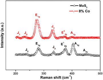 |
| | Fig. 2 Different Raman modes showing the presence of 1T and 2H phases in undoped and 8% Co doped MoS2. | |
Table 1 Variation of characteristic Raman modes of undoped and 8% Co doped MoS2 NFs
| Co doping percentage (%) |
E12g (cm−1) |
A1g (cm−1) |
Δk (cm−1) |
FWHM ratio (A1g/E12g) |
| 0 |
377.72 |
404.27 |
26.55 |
0.82 |
| 8 |
374.78 |
402.32 |
27.54 |
1.62 |
3.3. Morphology and microstructure study
3.3.1. SEM image analysis.
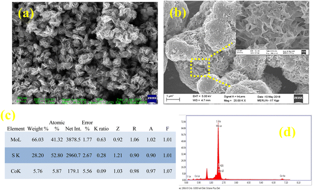
Fig. 3(a and b) show the FESEM images of the as-prepared 8% Co-doped MoS2 nanoflakes indicating the formation of a 3D hierarchical fluffy petaloid architecture. Each flower consists of several interconnected nanopetals in the form of nanoflakes. The average diameter of the undoped and 8% Co-doped MoS2 flowers is about ∼200 nm and ∼1.5 μm, lateral dimensions are ∼130 nm and ∼240 nm and the thickness lies within 10 nm. The lateral size of the MoS2 NF increases with the incorporation of more Co dopants. The reason for the formation of larger nanoflowers with higher dopant content may be ascribed to the accumulation of dopant and defect-induced charge on the surface and edge of the lamellar structure contributing to the electrostatic attraction between them which can be validated by zeta potential measurements.40Fig. 3(c and d) show the EDAX elemental data analysis and plot indicating the proper distribution and presence of Mo, S and Co in 8% Co-doped MoS2 NFs. However the theoretically calculated stoichiometric ratio of Co, Mo, and S (0.03![[thin space (1/6-em)]](https://www.rsc.org/images/entities/char_2009.gif) :
:![[thin space (1/6-em)]](https://www.rsc.org/images/entities/char_2009.gif) 0.31
0.31![[thin space (1/6-em)]](https://www.rsc.org/images/entities/char_2009.gif) :
:![[thin space (1/6-em)]](https://www.rsc.org/images/entities/char_2009.gif) 0.66) for 8% Co-doped MoS2 matches well with the experimentally found value with a slight variation (0.05
0.66) for 8% Co-doped MoS2 matches well with the experimentally found value with a slight variation (0.05![[thin space (1/6-em)]](https://www.rsc.org/images/entities/char_2009.gif) :
:![[thin space (1/6-em)]](https://www.rsc.org/images/entities/char_2009.gif) 0.41
0.41![[thin space (1/6-em)]](https://www.rsc.org/images/entities/char_2009.gif) :
:![[thin space (1/6-em)]](https://www.rsc.org/images/entities/char_2009.gif) 0.53) possibly due to the presence of S vacancies.
0.53) possibly due to the presence of S vacancies.
 |
| | Fig. 3 SEM images of (a) undoped and (b) 8% Co doped MoS2 nanostructures. The inset of (b) shows a zoomed view of the encircled area indicating the microstructure of nanoflakes after doping. (c and d) EDAX analysis of 8% Co doped MoS2 indicating the percentage of Mo, Co and S elements present in the sample. | |
3.3.2. TEM image analysis.
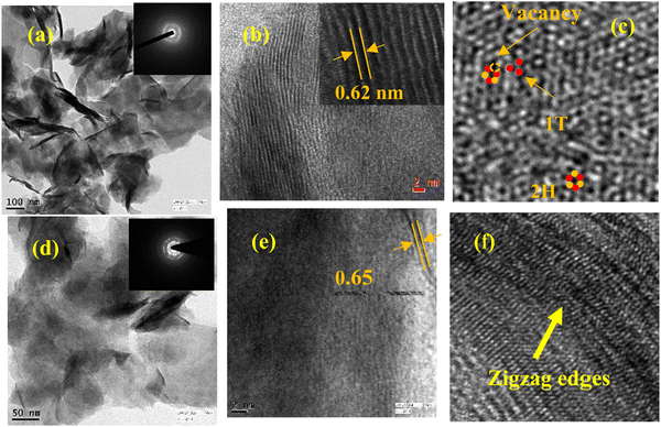
The detailed information about the microstructure of undoped and 8% Co-doped MoS2 NFs can be further unfolded by TEM image analysis. The thin interlaced flakes of MoS2 convert to a bigger nanostructure having sheet-like morphology with larger lateral dimensions which can be well understood in Fig. 4(a and d). The inset of Fig. 4(a) shows diffused rings in the SAED pattern of undoped MoS2 whereas the inset of Fig. 4(d) shows distinct spots in SAED pattern diffraction planes indicating an increased crystalline nature upon doping in 8% Co-doped MoS2. Fig. 4(b) clearly shows the magnified image of interlaced flakes of undoped MoS2 where the interlayer distance is found to be ∼0.62 nm forming a 14–16-layer system. In the case of 8% Co-doped MoS2, it has been observed that the number of layers lies within 4–8 layers having an extended interlayer distance ∼0.65 nm as shown in Fig. 4(e) due to the appearance of doping-induced lattice strain.39Fig. 4(c) shows the prominent presence of 2H and 1T phases and defects in the vicinity of the 1T phase. The presence of edge-terminated zigzag orientation in 8% Co-doped MoS2 has been indicated by an arrow as shown in Fig. 4(f). According to Tinico et al., such type of zigzag orientation in vertically oriented MoS2 is responsible for metallic behaviour.62
 |
| | Fig. 4 TEM images showing (a and b) thin nanoflake like morphology and interplanar spacing (0.62 nm) of undoped MoS2, (c) prominent presence of 2H and 1T phases and sulfur vacancies (Vs, encircled) in 8% Co doped MoS2, (d) interlaced flakes forming larger nanoflakes of 8% Co MoS2, and (e and f) the extended interplanar spacing (0.65 nm) and presence of zigzag edges in 8% Co doped MoS2. | |
3.4. XPS study
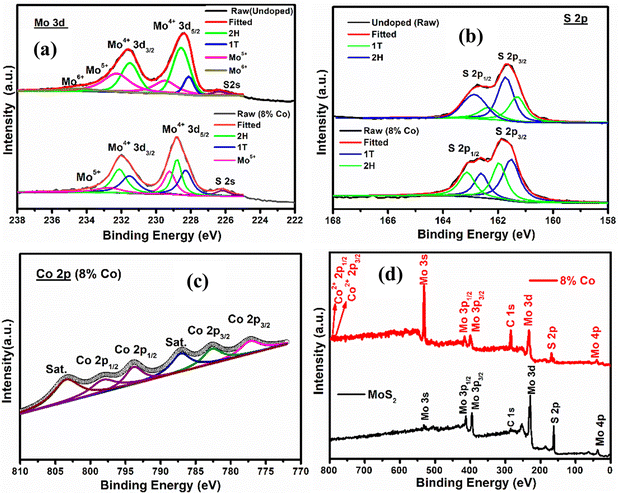
The chemical composition and prominent presence of the 1T phase along with the 2H phase in undoped40 and 8% Co-doped MoS2 have been verified by X-ray photoelectron spectroscopic (XPS) measurement. The typical BE peaks of Mo 3d5/2 and Mo 3d3/2 corresponding to the 2H phase of 8% Co-doped MoS2 appeared at 228.37 and 231.75 eV, as shown in Fig. 5(a). Two extra peaks corresponding to Mo 3d5/2 and 3d3/2 of the 1T characteristic phase were shifted to ∼0.5–1 eV. Similarly, the binding energy peaks corresponding to S 2p3/2 and S 2p1/2 of the 2H phase appeared at 161.63 and 162.79 eV in the case of 8% Co-doped MoS2, as shown in Fig. 5(b). Two other extra peaks shifted about ∼0.5 eV from S 2p3/2 and S 2p1/2 of the 2H phase are assigned to the 1T phase. It has been observed that the doublets corresponding to Mo4+ and S2− are shifted to lower binding energy with a gradual increase of Co dopant as observed in 8% Co-doped MoS2 when compared with the undoped one as shown in Fig. 5(a and b), confirming the loss of sulfur atoms in the sample.58 The difference between Mo 3d3/2 and 3d5/2 binding energy peaks corresponding to the 1T phase is 3.1 eV confirming the emergence of Mo5+ ions in 8% Co-doped MoS2.63 By analyzing the XPS spectra, the S![[thin space (1/6-em)]](https://www.rsc.org/images/entities/char_2009.gif) :
:![[thin space (1/6-em)]](https://www.rsc.org/images/entities/char_2009.gif) Mo peak ratio for 4% Co-doped MoS2 is 37% smaller than that for 2% Co-doped MoS2 NFs.64 In addition, based on the analysis of the Mo 3d peak area, it is deduced that the content of Mo5+ in MoS2 NFs is around 26%, demonstrating a defect-rich structure.65 Four main peaks corresponding to Co 2p3/2 at 780.34 eV (Co3+) and 785.27 eV (Co2+) and Co 2p1/2 at 791.33 eV (Co3+) and 798.07 eV (Co2+) are found in 8% Co-doped MoS2 as shown in Fig. 3(c) similar to the report in the case of Co species found in CoS2.66–69 Also, another two peaks arising at 790.73 eV and 803.24 eV signify the existence of satellite shake-up peaks. The binding energy peak of Co 2p3/2 at 780.34 eV resembles the CoMo2S4 phase, confirming the uniform substitution of Mo atoms by Co2+ along the {002} or the S-edge planes.70 The presence of the elements C, Mo, S, O and Co is revealed in the survey spectrum (wide scan) of undoped and 8% Co-doped MoS2 as shown in Fig. 5(d). The BE peaks corresponding to different oxidation states of Mo, S, and Co elements present in our samples are listed in Table 2.
Mo peak ratio for 4% Co-doped MoS2 is 37% smaller than that for 2% Co-doped MoS2 NFs.64 In addition, based on the analysis of the Mo 3d peak area, it is deduced that the content of Mo5+ in MoS2 NFs is around 26%, demonstrating a defect-rich structure.65 Four main peaks corresponding to Co 2p3/2 at 780.34 eV (Co3+) and 785.27 eV (Co2+) and Co 2p1/2 at 791.33 eV (Co3+) and 798.07 eV (Co2+) are found in 8% Co-doped MoS2 as shown in Fig. 3(c) similar to the report in the case of Co species found in CoS2.66–69 Also, another two peaks arising at 790.73 eV and 803.24 eV signify the existence of satellite shake-up peaks. The binding energy peak of Co 2p3/2 at 780.34 eV resembles the CoMo2S4 phase, confirming the uniform substitution of Mo atoms by Co2+ along the {002} or the S-edge planes.70 The presence of the elements C, Mo, S, O and Co is revealed in the survey spectrum (wide scan) of undoped and 8% Co-doped MoS2 as shown in Fig. 5(d). The BE peaks corresponding to different oxidation states of Mo, S, and Co elements present in our samples are listed in Table 2.
 |
| | Fig. 5 XPS narrow scan spectra of undoped and 8% Co doped MoS2 (a) Mo 3d, (b) S 2p and (c) Co 2p of 8% Co MoS2. Survey spectra of Mo (3d, 3p, 3s), S 2p, C 1s, and Co 2p are shown in (d) corresponding to undoped and 8% Co doped MoS2. | |
Table 2 Position of binding energy peaks of Mo, S and Co elements corresponding to the 1T and 2H phase of undoped and 8% Co-doped MoS2
| Doping amount (%) |
1T |
2H |
1T |
2H |
Co3+ |
Co2+ |
| Mo 3d5/2 (eV) |
Mo 3d3/2 (eV) |
Mo 3d5/2 (eV) |
Mo 3d3/2 (eV) |
S 2p3/2 (eV) |
S 2p1/2 (eV) |
S 2p3/2 (eV) |
S 2p1/2 (eV) |
Co 2p3/2 (eV) |
Co 2p1/2 (eV) |
Co 2p3/2 (eV) |
Co 2p1/2 (eV) |
| 0 |
228.2540 |
231.1240 |
22940 |
231.540 |
161.740 |
162.040 |
162.9640 |
163.3740 |
— |
— |
| 8 |
227.88 |
231.25 |
228.37 |
231.75 |
161.17 |
162.31 |
161.63 |
162.79 |
780.34 |
791.33 |
785.27 |
798.07 |
3.5. Electronic transport property study
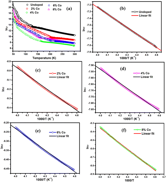
Fig. 6 shows the temperature-dependent resistivity curves for all undoped and Co-doped MoS2, exhibiting typical semiconductor behaviour. The resistivity eventually decreases with an increase in doping concentration and it is clearly seen in low-temperature regimes. This supports the increase in carrier concentration with the incorporation of an increased proportion of the 1T phase with Co doping.71 Thermal excitation of electrons from donor levels to the conduction band takes place with the increase in temperature. Temperature-dependent resistance can be written in an Arrhenius form:
σ(T) = σ0![[thin space (1/6-em)]](https://www.rsc.org/images/entities/char_2009.gif) exp(−Ea/kBT) exp(−Ea/kBT) |
where σ is the conductivity, σ0 is the pre-exponential factor, kB is the Boltzmann constant, and Ea is the activation energy. Fig. 6(a–f) shows the plots of the conductivity in log scale as a function of 1000/T from 217 K to 250 K of undoped and 2%, 4%, 6%, and 8% Co-doped samples. Different thermal activation energy regions have been obtained beyond 200 K. The data are fitted to a line with different slopes in this temperature region. The activation energy values for undoped and 2%, 4%, 6% and 8% Co-doped samples are 85.13 meV, 65.73 meV, 47.38 meV, 33.9 meV and 85.3 meV respectively (above 200 K). The activation energy is observed to be much lower than the band gap energy of MoS2 samples. Such low activation energy strongly suggests that native defects such as sulfur vacancies and impurities are present in the as-synthesized MoS2 samples as already verified in the XPS result. The decrease of activation energy with an increase of doping concentration suggests that donor carrier density lifts the Fermi level position in the band gap which supports the result obtained from UV-visible absorption spectra.40 It has been studied in a doped semiconductor that a major portion of the free electrons is recaptured by donor atoms themselves at low temperatures.72 The electrons suffer from lack of sufficient energy to jump from donor levels to the conduction band. At this stage, the electrons transport through hopping from one level to another in the impurity band and free-electron band conduction becomes less significant.72 Thermal activation is due to deep donor level ions contributing to the conduction band. For higher cobalt doped MoS2 at temperature <200 K, the activation energy (Ea) drops and other transport mechanisms could play a role in addition to the nearest neighbour hopping. The weak temperature dependence of resistance at low temperatures can be explained by the mechanism of electron hopping through impurity levels formed near the conduction band edge of cobalt-doped MoS2. In addition to this, the decrease of temperature is accompanied by a rapid rise of electrical resistivity as electrons hop from the conduction band to the localized impurity states. Therefore, the conduction mechanisms in these Co-doped MoS2 samples can be explained by the combination of two types of conduction models such as variable range hopping (VRH), σVRH = σ0VRH exp [−(T0VRH/T)1/4], and thermal excitation by nearest neighbour hopping (NNH), σth = σ0th exp[(Ea/kT)], where σ0VRH, T0VRH, and σ0th are constants. The first one describes carrier hopping in localized states at a lower temperature range whereas the second one describes carriers that have been thermally excited from the localized state to the conduction band. The parameters were evaluated from the linear fitting method by plotting ln![[thin space (1/6-em)]](https://www.rsc.org/images/entities/char_2009.gif) σ ∼ T−1/4(VRH) and ln
σ ∼ T−1/4(VRH) and ln![[thin space (1/6-em)]](https://www.rsc.org/images/entities/char_2009.gif) σ ∼ 1000/T(NNH) in different temperature regions to investigate the involved temperature-dependent transport processes. These parameters are listed in Table 3. The resistivity rises at low temperature and passes the VRH test for 2%, 4%, and 8% Co-doped samples (50–70 K) and for 6% Co (50–110 K) at a low-temperature range as shown in Fig. 7(a, b, d and c), respectively. It suggests that the conduction in these pellet-formed powder samples is due to the thermally assisted tunneling of the charge carriers through the grain boundary barrier and transition from the donor level to the conduction band. It is observed that at low temperature, the resistivity of 8% Co-doped MoS2 is very less compared to the undoped one due to incorporation of the metallic 1T phase in 2H MoS2 with the increase of cobalt doping concentration. Increasing the Co-doping concentration will reduce the resistance, and in Table 3 it has been observed that the activation energy decreases from 65.73 meV to 33.59 meV as the concentration of Co atoms increases from 2% to 6%. It has been observed that in the case of heavy doping of the Co ion (8% Co) in MoS2, the activation energy is increased. This is attributed to the increase in atomic defects which are electrically active at the grain boundary.73
σ ∼ 1000/T(NNH) in different temperature regions to investigate the involved temperature-dependent transport processes. These parameters are listed in Table 3. The resistivity rises at low temperature and passes the VRH test for 2%, 4%, and 8% Co-doped samples (50–70 K) and for 6% Co (50–110 K) at a low-temperature range as shown in Fig. 7(a, b, d and c), respectively. It suggests that the conduction in these pellet-formed powder samples is due to the thermally assisted tunneling of the charge carriers through the grain boundary barrier and transition from the donor level to the conduction band. It is observed that at low temperature, the resistivity of 8% Co-doped MoS2 is very less compared to the undoped one due to incorporation of the metallic 1T phase in 2H MoS2 with the increase of cobalt doping concentration. Increasing the Co-doping concentration will reduce the resistance, and in Table 3 it has been observed that the activation energy decreases from 65.73 meV to 33.59 meV as the concentration of Co atoms increases from 2% to 6%. It has been observed that in the case of heavy doping of the Co ion (8% Co) in MoS2, the activation energy is increased. This is attributed to the increase in atomic defects which are electrically active at the grain boundary.73
 |
| | Fig. 6 Logarithmic plot of resistivity with temperature of (a) undoped and Co doped MoS2. Linear variation of conductivity with inversion of temperature to test the (b) undoped and (c) 2%, (d) 4%, (e) 6% and (f) 8% Co doped MoS2 which satisfy the thermal excitation process of transport. | |
Table 3 Various transport mechanisms in different temperature regimes observed in cobalt doped MoS2
| Samples |
σ
0VRH (Ω m)−1 |
T
0VRH (K) |
σ
0EVRH (Ω m)−1 |
T
0EVRH (K) |
σ
0Th (Ω m)−1 |
E
A (meV) |
Adj. R2 |
Temperature coefficient of resistance (TCR) (K−1) |
| MoS2 |
— |
— |
— |
— |
3.7397 |
85.13 |
0.9998 |
−3.74 × 10⁻² |
| 2% Co |
3.932 × 10⁹ |
1.67 × 10⁸ |
352.7 |
30043.28 |
0.2686 |
65.73 |
0.99825 |
−3.12 × 10⁻² |
| 4% Co |
5.92 × 10¹¹ |
1.08 × 10⁷ |
6.5023 |
9583.31 |
0.4832 |
47.37 |
0.99828 |
−1.85 × 10⁻² |
| 6% Co |
0.7780 |
2![[thin space (1/6-em)]](https://www.rsc.org/images/entities/char_2009.gif) 931 931![[thin space (1/6-em)]](https://www.rsc.org/images/entities/char_2009.gif) 986 986 |
7.5341 |
12![[thin space (1/6-em)]](https://www.rsc.org/images/entities/char_2009.gif) 500 500 |
0.1267 |
33.59 |
0.99871 |
−1.29 × 10⁻² |
| 8% Co |
5597.07 |
2.673 × 10⁷ |
1.769 |
18770.31 |
0.00647 |
85.3 |
0.9997 |
−2.93 × 10⁻² |
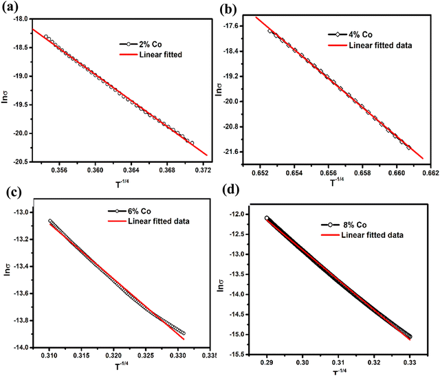 |
| | Fig. 7 Temperature dependent conductivity plot of 2%, 4%, 6% and 8% Co doped MoS2 (a–d) and ln![[thin space (1/6-em)]](https://www.rsc.org/images/entities/char_2009.gif) σ ∼ T−1/4 plot of 2%, 4%, 6% and 8% Co doped MoS2 to test the VRH mechanism. σ ∼ T−1/4 plot of 2%, 4%, 6% and 8% Co doped MoS2 to test the VRH mechanism. | |
3.6. EPR analysis
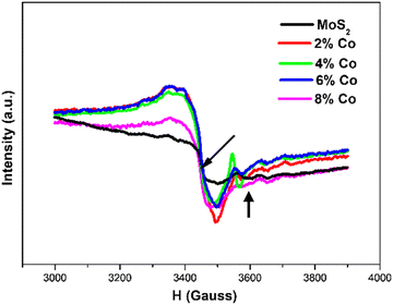
The room temperature electron paramagnetic resonance spectra (EPR) of MoS2 nanostructures doped with various percentages of cobalt are shown in Fig. 8. The undoped MoS2 shows a prominent resonant peak of low intensity at a magnetic field of 3446 G with g = 2.0005. This signal may come from the unpaired electrons generated by unsaturated coordination structures, e.g., vacancies and defects such as S vacancies, acting as paramagnetic centers.74 The EPR signal in the higher magnetic field is indicated with an arrow in Fig. 8 at g = 1.89, which is very close to g values of oxygenated species of Mo5+ in amorphous or unsupported sulfides.74 The maximum EPR signal has been observed in 2% Co-doped MoS2 NFs and decreases gradually with an increase in Co dopant amount. The expression
is used to calculate the electron g factors, where ν = 9.65 GHz (frequency), h = 4.135 × 10⁻¹⁵ eV s−1 (Planck constant), β = 5.788 × 10⁻⁵ eV T−1 (Bohr magnetron) and H0 is the resonance magnetic field. Co doping at different concentrations in MoS2 does not induce any new peak or change in the EPR spectra. However, a peak shift towards a lower magnetic field has been observed in all the doped MoS2 samples. In Fig. 8, the prominent resonance peaks are witnessed at the magnetic field of 3435 G (g = 2.007), 3433 G (g = 2.008), 3439 G (g = 2.005), and 3443 G (g = 2.002) for 2 at% Co, 4 at% Co, 6 at% Co and 8 at% Co-doped MoS2 samples, respectively, which are attributed to the enhanced ferromagnetic coupling with the increase in Co concentration. Eventually, the g value reaches a maximum for 4 at% Co-doped MoS2. The 1T regions tend to produce more Mo4+ spins by expanding in the less dense S vacancy regions. However, in the case of higher cobalt concentration (8 at%), the proportion of the 1T phase has increased up to 48%. In this case, S atoms are surrounded by a majority of the Mo atoms compared to S vacancies whereas a few of Mo atoms exist as isolated Mo4+ spins. This explains the origin of the ferromagnetic coupling with S atoms, resulting in a rise of ferromagnetism in MoS2 nanoflakes macroscopically.31
 |
| | Fig. 8 EPR spectra of MoS2 NFs doped with various percentages of cobalt. | |
3.7. VSM data analysis
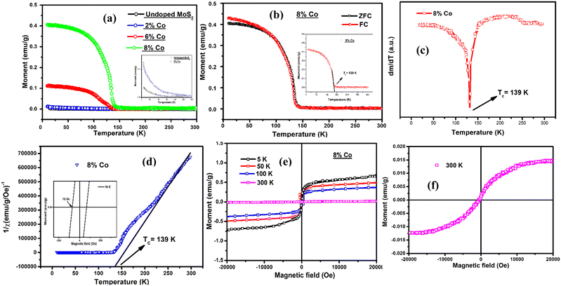
The magnetic properties (M–T and M–H at 10 K, 100 K and 300 K) of undoped and 2% Co, 6% Co and the highest Co (8% at wt.) doped MoS2 samples were studied through VSM as shown in Fig. 9. Both undoped and 2% Co-doped MoS2 samples show paramagnetic behaviour originating from free electrons contributed from defects and a small proportion of the 1T phase whereas 2% Co-doped MoS2 samples show higher magnetic moment compared to the undoped one as shown in the inset of Fig. 9(a). As reported by Nair et al. the existence of point defects such as vacancies and the introduction of fluorine adatoms in graphene induce notable paramagnetism.75 However, a paramagnetic to ferromagnetic transition has been distinctly found above 2% Co doping. The ZFC–FC feature in the M–T curve of 8% Co-doped MoS2 NFs, as shown in Fig. 9(b), almost retraces the same path indicating intrinsic single-phase ferromagnetism. The highest saturation magnetization (MS) at 10 K is 0.42 emu g−1 and 1.2 emu g−1, remanence magnetization (Mr) is 0.06 emu g−1 and 0.045 emu g−1 and coercivity is ∼150 Oe and 70 Oe corresponding to 6% Co- and 8% Co-doped MoS2 nanoflakes respectively as shown in Fig. S2(c) (ESI†) and Fig. 9(d). Since our undoped MoS2 possesses a feeble paramagnetic nature, it is fair to assume that the robust magnetism in 6% Co- and 8% Co-doped MoS2 arises as a consequence of doping. The magnetism in multilayer MoS2 and its doped analogues depends on the presence of zigzag edges, defect type, vacancies, lattice strain, and dopant concentration. Theoretical calculations by Wang et al.76 revealed that low concentration Co doping at 4% and 6% in the Mo vacant sites of the basal planes results in stable magnetic moments at room temperature. Yun et al.77 and Saab et al.78 also reported tuning of electronic and magnetic properties due to doping of metal ions in the MoS2 lattice. The high MS observed in Co-doped MoS2 suggests that the robust ferromagnetism here originates not from the strain in the layer but rather from the ferromagnetically favourable ordering of Co2+ ions.50 The effective Bohr magneton number (peff(Co)) and the value of the Curie constant (C) were calculated using the following formulae:| | | (peff(Co))2 = xg2S(Co2+)(S(Co2+) + 1) + (1 − x)g2S(Co3+)(S(Co3+) + 1) | (1) |
| | | (peff(Co))2 = 3Ck/NμB2 | (2) |
where g = 2 represents the Lande’ g-factor of the cobalt ions, S(Co2+) and S(Co3+) represent the total spin quantum numbers for Co2+ and Co3+ ions respectively, k is the Boltzmann constant, N is the Avogadro number and μB is the Bohr magneton. The value of peff(Co) obtained for MoS2 NFs doped with various amounts of cobalt lies between the theoretical value of peff(Co2+) = 3.87 and peff(Co3+) = 4.89 due to the presence of the mixed-valence state of Co in Co-doped MoS2 NFs. Again, the value of Curie temperature of 6% and 8% Co-doped MoS2 NFs was obtained from the minima of the dm/dT vs. T plot. The magnitude of the Curie constant (C) for 6% and 8% Co-doped MoS2 nanoflakes was calculated using eqn (2) by putting the value of peff(Co). The variation of saturation magnetization (Ms), Curie temperature (Tc), Curie constant (C), peff(Co) and the percentage amount of Co2+/Co3+ ions present in MoS2 NFs doped with various amounts of cobalt are listed in Table 4.
 |
| | Fig. 9 (a) M vs. T plot of undoped and 2%, 6% and 8% Co doped MoS2 at an applied field of 500 Oe; the inset shows the M–T curve of undoped and 2% Co doped MoS2. (b) Individual ZFC–FC curve of 8% Co doped MoS2 indicating Tc ∼ 139 K. (c) dm/dT plot of 8% Co doped MoS2 showing Tc ∼ 139 K. (d) Linearly fitted 1/χ ∼ T (Tc ∼ 139 K) corresponding to 8% Co doped MoS2; the inset shows a magnified image of the M vs. H hysteresis loop of 8% Co doped MoS2 at 10 K having 70 Oe coercive field. (e) Hysteresis loop at 10 K, 50 K, 100 K and 300 K. (f) M–H loop of 8% Co doped MoS2 showing room-temperature ferromagnetism at 300 K at a magnified scale. | |
Table 4 Variation of magnetic parameters with various amounts of Co doping (0%, 2%, 6%, 8%) in Co-doped MoS2 NFs
| Doping percentage (%) |
M
s (emu g−1) |
T
c (K) |
C (emu K Oe−1 mol−1) |
p
eff(Co2+, Co3+) (calculated) |
Variation of Co2+/Co3+ ions in percentage with Co doping |
| Co2+ |
Co3+ |
| 0 |
— |
— |
— |
— |
— |
— |
| 2 |
— |
— |
2.24 |
4.26 |
65 |
35 |
| 6 |
0.42 |
131 |
2.32 |
4.32 |
59 |
41 |
| 8 |
1.2 |
139 |
2.45 |
4.37 |
54 |
46 |
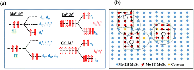
To study the origin and variation of the observed ferromagnetism in MoS2 NFs with Co doping, it is necessary to point out the role of the 1T phase and cobalt ion incorporation in the 2H MoS2 matrix. The fact that Co dopant atoms can effectively introduce ferromagnetism in MoS2 nanoflakes has been confirmed by magnetic measurement results. Herein, we only consider the magnetic moment introduced in the MoS2 NFs through the substitution of Mo atoms by Co atoms. According to crystal field theory, 4d and 3d orbitals corresponding to Co2+/Co3+ remain in different degenerate states in 2H and 1T coordination.31 The Mo4+ ions corresponding to 2H coordination split into three energy levels: (dz2), (dx2−y2, dxy), and (dxz, dyz) while the 1T has two levels: (dxz, dyz, dxy) and (dx2−y2, dz2) as shown in Fig. 10(a). As described in Fig. 10(a), two 4d electrons occupy the dz2 orbital of the Mo4+ ion in a spin-antiparallel manner, thus giving net zero magnetic moments in the 2H phase. In the case of the 1T phase of MoS2, the lower energy levels (dxz, dyz, dxy) are occupied by the two 4d electrons spin-parallelly contributing net magnet moments in the 1T phase of Mo atoms.79 Therefore, it can be assumed that the presence of ferromagnetism is directly connected to the proportion of both 1T and 2H phases in MoS2 nanoflakes. Seven and six 3d electrons corresponding to the Co2+ and Co3+ configuration contribute three and four unpaired electrons in the octahedral geometry of the Co2+ and Co3+ configuration, respectively. The observed magnetic moment varies monotonically with the proportion of the 1T phase present in the sample. In undoped MoS2, the proportion of the 1T phase was 18% having the lowest magnetic moment as shown in EPR analysis. The proportion of the 1T phase increases gradually with the incorporation of the cobalt dopant. The proportion of the 1T phase in undoped and 2%, 4%, 6% and 8% Co-doped MoS2 samples is found to be 18%, 26%, 39%, 42% and 48%, respectively. The magnetic moment value increases as the proportion of the 1T phase increases with an increase in the cobalt dopant as revealed by experimental results.
 |
| | Fig. 10 (a) Electron orbital degenerate states of Mo atoms (Mo4+ ionic state) in 1T and 2H configuration and Co atoms (Co2+ and Co3+ ionic state). (b) Schematic representation of the bound magnetic polaron model mediated by vacancy and Co dopant in MoS2 NFs. 1T phases are induced around vacancy and Co atom forming spin polarized states. | |
To further explain the origin of ferromagnetism in Co-doped MoS2 systems, the bound magnetic polaron (BMPs) model is utilized.80–82 Two main results are obtained from the XPS spectra: (i) S vacancies are typical defects in hydrothermally synthesized MoS2 nanoflakes and (ii) the substituted Co atoms can contribute two holes. Thus the Co2+ dopants provide the local magnetic moments in addition to the carriers needed to couple these moments.80 Under this condition, the electron distribution changes causing a strong interaction among the spin impurities. Unintentional sulfur vacancies are formed in MoS2 nanoflakes during the hydrothermal synthesis process. As a result, BMPs could be realized with localized holes and the S vacancies surrounded by a large number of Mo4+ spins.80 The Mo4+ spins and S vacancy spin are aligned parallel, leading to the formation of a BMP. Cai et al. observed that the 2H–1T phase transformation always occurs near the defects.52 Such ferromagnetism appears due to the overlapping of BMPs and their ferromagnetic coupling to each other as shown in Fig. 10(b).
Additionally, with the Mo4+ ions, the doped Co ions can be bounded by the S vacancies82,83 as shown in Fig. 10(b). Only those Co ions arranged at suitable distances can interact ferromagnetically possibly through some indirect coupling mechanism.50 In this manner, numerous BMPs can be created by the Co ions in the vicinity of the S vacancies. They are ordered ferromagnetically and establish long-range room-temperature ferromagnetism in Co-doped MoS2 nanoflakes.84
3.8. Theoretical result
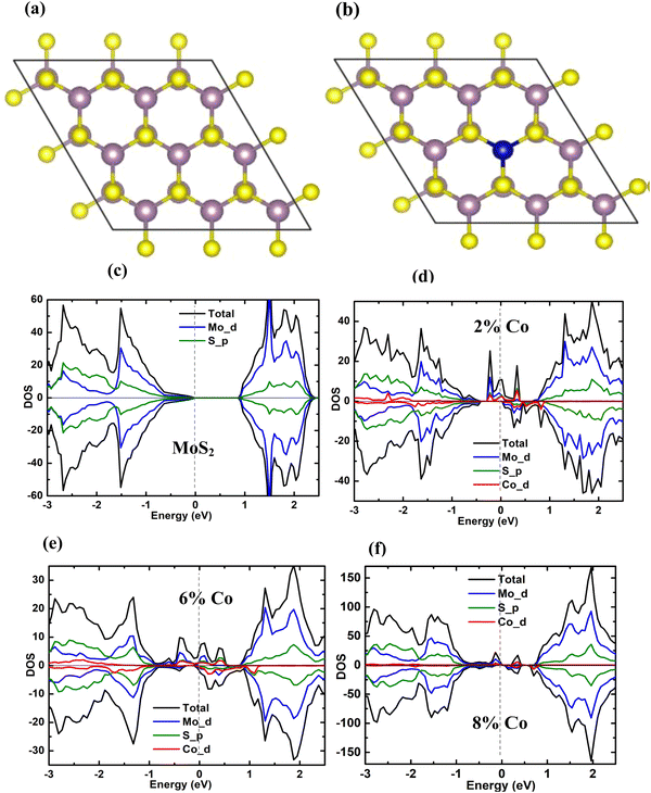
To simulate 2%, 6% and 8% Co doping in MoS2, 5 × 5 × 1, 3 × 3 × 1 and 3 × 2 × 1 bulk MoS2 supercells were created respectively and then one Mo atom from the supercell was substituted with one Co atom, to incorporate the desired doping level, as shown in Fig. 11(a and b). The average Mo–Mo and Mo–S bond length obtained theoretically from our calculation agrees well with the experimental value85 in the case of undoped and doped samples. In all the doped cases a small variation of the average Co–Mo bond length values and the average Mo–Mo bond length around the dopant site is observed from the Mo–Mo bond length value in the undoped cases. This suggests that the substitutional doping of Co at Mo does not change the symmetry around the dopant site. All the calculations are performed on the semiconducting 2H phase, since this phase is seen to be the dominant one over the metallic 1T phase, in all the cases.
 |
| | Fig. 11 The atomic structure of (a) the undoped MoS2 supercell and (b) the 3 × 3 × 1 supercell of 6% Co doped MoS2 from top view with a Co atom substituting the Mo site. The big purple balls represent Mo atoms, small yellow balls represent sulphur atoms and the blue ball represents the cobalt atom. The projected density of states (PDOS) corresponding to Mo d, S p and Co d states of (c) the undoped MoS2 supercell, (d) the supercell with 2% Co dopant, (e) the supercell with 6% Co dopant and (f) the supercell with 8% Co dopant (the vertical dashed line indicates the Fermi level). | |
The total and projected densities of states (TDOS and PDOS) of undoped MoS2 and 2%, 6%, and 8% Co-doped MoS2 are displayed in Fig. S3(a–d) (ESI†) and Fig. 11(a–d), respectively. The symmetry of the spin-up and spin-down DOS throughout the energy range, as shown in Fig. 11(a), validates the nonmagnetic nature of the undoped MoS2 NFs. In the case of doped systems, it is seen that the doping of the Co atom in one layer does not affect the other layer. The reason might be the weak interlayer interaction and the large interlayer separation. The isolated Co atom possesses an electronic configuration of 3d74s2 having three additional valence electrons compared to the Mo atom, and it contributes to the magnetic moment in the Co-doped system. The overall magnetic moment of the supercell with one Co atom substituting one Mo atom and the local magnetic moment of the constituent atoms for 2%, 6%, and 8% Co-doped MoS2 NFs are presented in Table 5. The Co atom induces spin polarization in the neighbouring 6 Mo atoms and S atoms. The spins of the six neighbouring Mo atoms are coupled to the Co atom with an average moment of 0.2μB in the 6% Co-doped case. An average magnetic moment of 0.04μB is contributed by spin-polarized p orbitals of the S atoms. More obviously, the Co dopant site remains in trigonal prismatic symmetry even after structural relaxation. As shown in Fig. 11(c–f), with the doping of the Co atom replacing a Mo atom, a distinct spin splitting appears near the Fermi level contributing to large ferromagnetism. This is attributed to the defect states associated with the doped Co atom, p states of the adjacent S atoms, and d states of the nearby Mo atoms, although mainly Co-d and Mo-d states. Due to the overlapping among the Co-d, Mo-d, and S-p orbitals the band edge structures change significantly in comparison with undoped MoS2. For the C3v symmetry around the dopant site, the doping produces five 3d states within the band gap which split into three sub-levels e1, e2, and a, among which one is mono degenerate and two doubly degenerate. The Co e1 (dxy, dx2−y2) orbitals and e2 (dxz, dyz) orbitals are strongly hybridized with S 3p orbitals and remain at relatively low energy levels in the spin-up channel, whereas in the spin-down channel they possess higher energy.13 The 3 extra non-bonding valence electrons occupy the lowest energy mono-degenerate a (dz2) and the first doubly degenerate (dxy, dx2−y2) states in the spin-up channel. The spin-down channel remains vacant at the Fermi level, at least in the low doping regime. The results obtained from the calculation indicate an obvious asymmetry of the DOS around the Fermi level of the cobalt doped MoS2, confirming that the substitution of Co at the Mo site gives rise to the spin-polarized state. Interestingly, the DOS indicates that Co-doped MoS2 exhibits half-metallic behaviour in the 2% doping case, i.e., the DOS shows no gap in the spin-up channel and a semiconducting band gap in the spin-down channel which means being a semiconductor in one spin channel and a metal in another.13,86,87 It is obvious from the calculation that, the asymmetry around the Fermi level has increased significantly with the increase in Co dopant concentrations, resulting in a net increase of total magnetic moment. Experimentally it has been demonstrated that Co doping up to a certain percentage can enhance ferromagnetism very well. The theoretical calculation for the Co doping in the dominant phase 2H supercell of MoS2 shows the increasing nature of magnetic moment with an increase in doping concentration which supports the experimental evidence obtained from VSM measurements. This is probably because the small contribution of the 1T phase has been neglected in the calculation since the 2H phase has always been the dominant one over the 1T phase. However, the calculation presents a clear picture of the environment around the dopant site, the local and global magnetism and the induction of magnetism from the dopant to the nearby Mo and S atoms. To visualize the nature of the impurity state initiated by the S defect, Salehi et al.88 discussed the influence of chalcogen defect on the electronic structure of the monolayer MoS2 by assuming a single sulphur vacancy per supercell. Evidently, at high defect concentration, a midgap band is introduced by the sulphur vacancies near the VBM having a bandwidth of ∼0.6 eV. Such types of defect states tend to become more delocalized due to the interaction between S vacancies. Additionally, a flat band appears just below the MoS2 CBM which does not change notably with the concentration changes. The Mo 4d orbitals around the vacancies play the main role in the creation of midgap states, while the S 3p and 3d orbitals do not contribute considerably to the defect states of the gap region. The presence of sulphur vacancies shifts the Fermi level to the bottom of the conduction band due to the unsaturated electrons in the Mo orbitals around the vacancy defect. In the case of multi-layered MoS2, the effect of layers and their interactions come into the picture. In the case of multi-layered MoS2 with S vacancy in each layer, an increase in the electron density of the unremoved S atoms has been observed which increases the repulsion of electrons between layers, increasing the interlayer distance as reported by Zhu et al.89 Additionally, a direct band gap with Γ → Γ transition is observed in addition to a decrease in the band gap by introducing mid-gap defect in the forbidden region for the MoS2 structures with S vacancies. This is quite different from the Γ → K transition as observed in bulk MoS2 without defects. In the MoS2 structures with S vacancies, the VBM is mainly composed of the 4d orbital of the Mo atom at the Γ point, while the doping band minimum is almost composed of the 4d orbital of the Mo atom and the 3p orbital of the S atom at the Γ point. This can be considered to be responsible for such direct nature of Γ → Γ transition. Such type of defect and 1T phase enriched Co-doped half-metallic MoS2 possessing robust ferromagnetism may show greater potential for application in spintronic and detection-based devices.
Table 5 Local magnetic moments of the dopant Co and the six neighbouring Mo and total magnetic moments in MoS2 multi-layered systems doped with various percentages of cobalt
| Doping percentage (%) |
Local magnetic moments (μB) |
Total magnetic moments |
| (μB) |
(emu g−1) |
| Mo |
Co |
| 0 |
0 |
— |
0 |
0 |
| 2 |
0.24 |
0.91 |
2.96 |
4.16 |
| 6 |
0.20 |
1.10 |
2.94 |
5.77 |
| 8 |
0.14 |
1.34 |
2.63 |
7.76 |
3.9. Electrochemical measurement
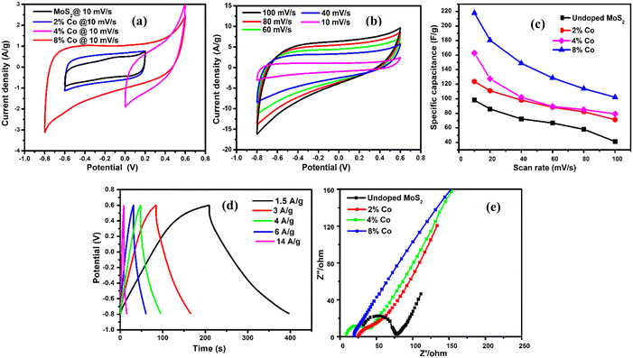
To unravel the effect of Co-doping on MoS2 NFs, the electrochemical performance of undoped MoS2 and 2% Co, 4% Co and 8% Co-doped MoS2 as electrode materials was characterized by cyclic voltammetry (CV), chronopotentiometry (CP) and electrochemical impedance spectroscopy (EIS) measurements. The measurement was performed with three-electrode equipment, which consists of Ag/AgCl as the reference electrode, Pt as the counter electrode and one glassy carbon electrode loaded with a sample on it as the working electrode. The prepared working electrode was analysed at different scan rates (10–100 mV s−1) within a potential window of −0.6 V to 0.2 V (undoped, 2% Co-doped), 0 V to 0.6 V (4% Co) and −0.8 V to 0.6 V (8% Co-doped MoS2) using a 1 M Na2SO4 electrolyte. The comparative CV representation of undoped and 2% Co, 4% Co and 8% Co-doped MoS2 at a scan rate of 10 mV s−1 is provided in Fig. 12(a). It is observed from Fig. 12(a) that 8% Co-doped MoS2 shows the highest CV area at 10 mV s−1 scan rate which indicates better electrochemical performance compared to other MoS2 moieties. Therefore, the CV plots of 8% Co-doped MoS2 at different scan rates (10, 20, 40, 60, 80, and 100 mV s−1) are depicted in Fig. 12(b). The variation of specific capacitance (calculated from the CV profile) at different scan rates of undoped and 2% Co, 4% Co and 8% Co-doped MoS2 is depicted in Fig. 12(c) and the corresponding numerical values are listed in Table S1 (ESI†). The greater capacitive behaviour of 8% Co-doped MoS2 is attributed to the following factors: (1) the presence of a more metallic 1T phase resulting in high electrical conductivity and low internal resistance; (2) 1T phase being more electrochemically active in the edge planes;90 and (3) increased defect levels,91 validated from XPS and steady-state UV-vis absorption spectra and BET surface area (for undoped and 8% Co-doped MoS2 the BET surface area is 33.84 m2 g−1 and 43.47 m2 g−1 respectively), facilitating charge transport and adsorption of transported ions within 8% Co-doped MoS2 leading to rapid redox reactions. The area under the CV curve shows a symmetric rectangular-like shape revealing the better choice for energy storage application as an ideal supercapacitor.92 The specific capacitance of the symmetrical supercapacitor was calculated from the CV profile following eqn (3):| |  | (3) |
where  is the area under the CV curve, m is the mass of the electrode materials, ν is the scan rate, and ΔV is the potential window taken. 8% Co-doped MoS2 shows the highest specific capacitance of 217.9 F g−1 at a voltage scan rate of 10 mV s−1 which is approximately 1.7, 1.5 and 1.3 times greater than that of undoped (98.1 F g−1), 2% Co, and 4% Co-MoS2 electrode (123.7 F g−1) materials, respectively. It has been observed that upon increasing the scan rate, the capacitive value decreases. Usually, at a higher scan rate, sufficient ion diffusion cannot take place within a constant time, and therefore, the capacitance value decreases.92,93 Similarly, the galvanostatic charge–discharge (GCD) technique was carried out to further evaluate the capacitance behaviour of as-synthesized materials at different current densities (Fig. 12(d) and Fig. S4(b, d and f), ESI†). The GCD curve of 8% Co-doped MoS2 shows the symmetric charging and discharging curve which reveals the good capacitive behaviour of the 8% Co-doped sample. The specific capacitance of the hybrid material was derived from the GCD curve following eqn (4):where I is the current (mA), Δt is the discharge time (s), m is the active electrode material (mg) and ΔV is the potential window (V). The specific capacitance values of undoped and 2% Co, 4% Co, and 8% Co doped MoS2 electrodes with varying current densities obtained from the GCD plot are listed in Table S2 (ESI†). It has been observed that specific capacitance values obtained from CV and GCD measurements are nearly the same which indicates validation of our measurements and stability of the as-prepared electrode materials. To better understand the reason for the improved electrochemical performance of 8% Co-doped MoS2, electrochemical impedance spectroscopy (EIS) of undoped and 2% Co, 4% Co and 8% Co-doped MoS2 in the frequency range of 1 Hz–100 kHz was performed (Fig. 12(e)). The prepared MoS2 nanostructures show the supercapacitor feature, i.e., a semicircle at higher frequencies, which is related to the surface area and electrical conductivity, and a straight line in the lower frequency region. The intercept on the real axis is ascribed to the equivalent series resistance (Rs), and the diameter of the semicircle corresponds to the charge transfer resistance (Rct) in the electrode/electrolyte system. The Rs values for undoped and 2% Co, 4% Co and 8% Co-doped MoS2 are 31.1 Ω, 24.8 Ω, 8.7 Ω and 18.9 Ω, respectively. With the increase in cobalt doping the Rs value decreases from low-doping (2% Co) to high-doping concentration (8% Co-doped MoS2) which confirms that Co doping has enhanced the electrical conductivity of MoS2 NFs. The 8% Co-doped MoS2 electrode exhibits the smallest semicircle, indicating that the electrode has lower charge transfer resistance than the other two electrodes because the existing 1T phase and more available active sites decrease the charge transfer resistance. The 8% Co-doped MoS2 electrode shows a nearly vertical shape because electrons could transfer fast as rapid ion diffusion occurs due to less resistance at the electrode–electrolyte interface. The low-frequency straight line shows the capacitive behaviour of MoS2 nanomaterials (Fig. 12(e)). The highest slope of the straight line parallel to the imaginary axis is obtained for 8% Co-doped MoS2, suggesting that 8% Co-doped MoS2 has optimal performance among the prepared MoS2 nanostructures. Table 6 presents the comparative electrochemical performance of MoS2 (pure or in composite form when used as a single electrode material), as published in previous works, with the results obtained from our highest Co-doped (8% Co) MoS2 NFs, indicating improved electrochemical behaviour of our material. Therefore, the doping-induced phase and defect engineering of MoS2 NFs for enhanced electrochemical property in supercapacitors paves the way toward the production of more efficient electrode materials by designing Co-doped 1T phase and defect-rich MoS2 ultrathin NF-based composites.
 |
| | Fig. 12 (a) Comparative CV curves of undoped and 2% Co, 4% Co and 8% Co doped MoS2 NFs, (b) CV scans of 8% Co doped MoS2 at different scan rates, (c) plot of specific capacitance at different scan rates for undoped and 2% Co, 4% Co and 8% Co doped MoS2, (d) GCD plot of 8% Co-doped MoS2 at different current densities, and (e) Nyquist plots of undoped and 2% Co, 4% Co and 8% Co doped MoS2 electrodes. | |
Table 6 Electrochemical performance of MoS2 and its derived electrodes in supercapacitors
| Nanostructured electrode material |
Electrolyte |
Specific capacitance (single electrode) |
Ref. |
| MoS2 nanosheets |
1 M KCl |
148 F g−1 at 1 A g−1 |
94
|
| MoS2/PEI–GO |
2 M Na2SO4 |
153.9 F g−1 at 1 A g−1 |
95
|
| MoS2/graphene |
1 M Na2SO4 |
270 F g−1 at 0.1 A g−1 |
96
|
| MoS2/graphene |
6 M KOH |
258 F g−1 at 2 A g−1 |
97
|
| MoS2/a-C |
6 M NaOH |
163.7 F g−1 at 0.5 A g−1 |
98
|
| MoS2/CNT |
1 M Na2SO4 |
74.05 F g−1 at 2 A g−1 |
99
|
| Carbon-MoS2 yolk−shell microspheres |
1 M Na2SO4 |
122.6 F g−1 at 1 A g−1 |
100
|
| 8% Co doped MoS2 |
1 M Na2SO4 |
201.4 F g−1 at 1.5 A g−1 |
This work |
4. Conclusion
The well-matched 1T phase incorporation in 2H-phase MoS2 NFs using Co as a dopant at different weight percentages (0%, 2%, 4%, 6%, 8%) has been successfully carried out via a facile one-step hydrothermal technique. The evolution of the 1T phase, defects and vacancies and introduction of zigzag edges with Co doping have been verified using Raman, TEM and XPS measurement techniques. The robust ferromagnetism with Co doping was shown to have originated from ferromagnetic exchange interaction of Mo4+ and Co2+ with sulfur vacancies via the BMP model and magnetic moment contributed from zigzag edges. The asymmetry nature of the DOS and spin splitting near the Fermi level of Co-doped MoS2 NFs contributed by d states of Mo and Co atoms and p states of neighbouring S atoms confirms that substitutional doping of the Co atom at the Mo site can effectively induce a spin-polarized state corresponding to ferromagnetism. The prominent feature of half-metallicity and formation of the defect level within the MoS2 band gap has been evidenced from DOS results. In addition, various types of transport mechanisms existing in the different temperature regime have been explained and fitted well in the temperature variation resistivity curves. Moreover, Co-doping in MoS2 shows better electrochemical performances due to the presence of more electrochemically active metallic 1T sites, edge defects, increased BET surface area and enhanced interlayer separation due to intercalated Co2+/Co3+ ions. This work demonstrates that Co-doped ferromagnetic 1T-MoS2 NFs are promising for constructing Co-doped 1T-MoS2-based heterojunctions for application in spintronic and detection-based devices as well as energy storage devices in the future.
Conflicts of interest
The authors declare no conflict of interest.
Acknowledgements
The authors acknowledge the XPS facility, Department of Physics, IIT Kharagpur, and Central Research Facility (CRF), IIT Kharagpur, for providing the infrastructural support for the characterization of the samples. R. Rahman would like to acknowledge the INSPIRE research fellowship provided by DST, India, to carry out the present research work.
References
- W. Bao, X. Cai, D. Kim, K. Sridhara and M. S. Fuhrer, High Mobility Ambipolar MoS2 Field-Effect Transistors: Substrate and Dielectric Effects, Appl. Phys. Lett., 2013, 102(4), 042104, DOI:10.1063/1.4789365.
- E. Singh, P. Singh, K. S. Kim, G. Y. Yeom and H. S. Nalwa, Flexible Molybdenum Disulfide (MoS2) Atomic Layers for Wearable Electronics and Optoelectronics, ACS Appl. Mater. Interfaces, 2019, 11(12), 11061–11105, DOI:10.1021/acsami.8b19859.
- B. Radisavljevic, M. B. Whitwick and A. Kis, Integrated Circuits and Logic Operations Based on Single-Layer MoS2, ACS Nano, 2011, 5(12), 9934–9938, DOI:10.1021/nn203715c.
- M. Azhagurajan, T. Kajita, T. Itoh, Y. G. Kim and K. Itaya, In Situ Visualization of Lithium-Ion Intercalation into MoS2 Single Crystals Using Differential Optical Microscopy with Atomic Layer Resolution, J. Am. Chem. Soc., 2016, 138(10), 3355–3361, DOI:10.1021/jacs.5b11849.
- K. S. Novoselov, D. Jiang, F. Schedin, T. J. Booth, V. V. Khotkevich, S. V. Morozov and A. K. Geim, Two-Dimensional Atomic Crystals, Proc. Natl. Acad. Sci. U. S. A., 2005, 102(30), 10451–10453, DOI:10.1073/pnas.0502848102.
- Q. H. Wang, K. Kalantar-Zadeh, A. Kis, J. N. Coleman and M. S. Strano, Electronics and Optoelectronics of Two-Dimensional Transition Metal Dichalcogenides, Nat. Nanotechnol., 2012, 7(11), 699–712, DOI:10.1038/nnano.2012.193.
- M. Chhowalla, H. S. Shin, G. Eda, L. J. Li, K. P. Loh and H. Zhang, The Chemistry of Two-Dimensional Layered Transition Metal Dichalcogenide Nanosheets, Nat. Chem., 2013, 5(4), 263–275, DOI:10.1038/nchem.1589.
- S. Mathew, K. Gopinadhan, T. K. Chan, X. J. Yu, D. Zhan, L. Cao, A. Rusydi, M. B. H. Breese, S. Dhar, Z. X. Shen, T. Venkatesan and J. T. L. Thong, Magnetism in MoS2 Induced by Proton Irradiation, Appl. Phys. Lett., 2012, 101(10), 102103, DOI:10.1063/1.4750237.
- Z. Zhang, X. Zou, V. H. Crespi and B. I. Yakobson, Intrinsic Magnetism of Grain Boundaries in Two-Dimensional Metal Dichalcogenides, ACS Nano, 2013, 7(12), 10475–10481, DOI:10.1021/nn4052887.
- H. Shi, H. Pan, Y.-W. Zhang and B. I. Yakobson, Strong Ferromagnetism in Hydrogenated Monolayer MoS2 Tuned by Strain, Phys. Rev. B: Condens. Matter Mater. Phys., 2013, 88(20), 205305, DOI:10.1103/PhysRevB.88.205305.
- Y. Li, Z. Zhou, S. Zhang and Z. Chen, MoS2 Nanoribbons: High Stability and Unusual Electronic and Magnetic Properties, J. Am. Chem. Soc., 2008, 16739–16744 CrossRef CAS.
- D. Gao, M. Si, J. Li, J. Zhang, Z. Zhang, Z. Yang and D. Xue, Ferromagnetism in Freestanding MoS2 Nanosheets, Nanoscale Res. Lett., 2013, 8(1), 129, DOI:10.1186/1556-276X-8-129.
- Q. Chen, Y. Ouyang, S. Yuan, R. Li and J. Wang, Uniformly Wetting Deposition of Co Atoms on MoS2 Monolayer: A Promising Two-Dimensional Robust Half-Metallic Ferromagnet, ACS Appl. Mater. Interfaces, 2014, 6(19), 16835–16840 CrossRef CAS.
- F. Ouyang, Z. Yang, X. Ni, N. Wu, Y. Chen and X. Xiong, Hydrogenation-Induced Edge Magnetization in Armchair MoS2 Nanoribbon and Electric Field Effects, Appl. Phys. Lett., 2014, 104(7), 071901, DOI:10.1063/1.4865902.
- J. D. Fuhr, A. Saúl and J. O. Sofo, Scanning Tunneling Microscopy Chemical Signature of Point Defects on the MoS2 (0001) Surface, Phys. Rev. Lett., 2004, 92(2), 4, DOI:10.1103/PhysRevLett.92.026802.
- A. Ramasubramaniam and D. Naveh, Mn-doped Monolayer MoS2: An Atomically Thin Dilute Magnetic Semiconductor, Phys. Rev. B: Condens. Matter Mater. Phys., 2013, 87(19), 1–7, DOI:10.1103/PhysRevB.87.195201.
- Y. Wang, L.-T. Tseng, P. P. Murmu, N. Bao, J. Kennedy, M. Ionesc, J. Ding, K. Suzuki, S. Li and J. Yi, Defects Engineering Induced Room Temperature Ferromagnetism in Transition Metal Doped MoS2, Mater. Des., 2017, 121, 77–84, DOI:10.1016/j.matdes.2017.02.037.
- J. He, K. Wu, R. Sa, Q. Li, Y. Wei, J. He, K. Wu, R. Sa, Q. Li and Y. Wei, Magnetic Properties of Nonmetal Atoms Absorbed MoS2 Monolayers Magnetic Properties of Nonmetal Atoms Absorbed MoS2 Monolayers, Appl. Phys. Lett., 2010, 082504, 2–5, DOI:10.1063/1.3318254.
- A. V. Krasheninnikov, P. O. Lehtinen, A. S. Foster, P. Pyykkö and R. M. Nieminen, Embedding Transition-Metal Atoms in Graphene: Structure, Bonding, and Magnetism, Phys. Rev. Lett., 2009, 102(12), 126807, DOI:10.1103/PhysRevLett.102.126807.
- Y. G. Zhou, P. Yang, Z. G. Wang, X. T. Zu, H. Y. Xiao and X. Sun, Electronic and Magnetic Properties of Substituted BN Sheets: A Density Functional Theory Study, Phys. Chem. Chem. Phys., 2011, 13, 7378–7383, 10.1039/c0cp02001j.
- Q. Su and Z. Wang, Controlling Magnetism of MoS2 Sheets by Embedding Transition-Metal Atoms and Applying Strain, Phys. Chem. Chem. Phys., 2013, 15, 18464–18470, 10.1039/c3cp52832d.
- X. L. Fan, Y. R. An and W.-J. Guo, Ferromagnetism in Transitional Metal-Doped MoS2 Monolayer, Nanoscale Res. Lett., 2016, 11(1), 154, DOI:10.1186/s11671-016-1376-y.
- Z. Xiang, Z. Zhang, X. Xu, Q. Zhang, Q. Wang and C. Yuan, Room-Temperature Ferromagnetism in Co Doped MoS2 Sheets, Phys. Chem. Chem. Phys., 2015, 17(24), 15822–15828, 10.1039/c5cp01509j.
- Y. Wang, S. Li and J. Yi, Electronic and Magnetic Properties of Co Doped MoS2 Monolayer, Sci. Rep., 2016, 6(March), 1–9, DOI:10.1038/srep24153.
- S. Tongay, S. S. Varnoosfaderani, B. R. Appleton, J. Wu and A. F. Hebard, Magnetic Properties of MoS2: Existence of Ferromagnetism, Appl. Phys. Lett., 2012, 101(12), 123105, DOI:10.1063/1.4753797.
- J. Červenka, M. I. Katsnelson and C. F. J. Flipse, Room-Temperature Ferromagnetism in Graphite Driven by Two-Dimensional Networks of Point Defects, Nat. Phys., 2009, 5(11), 840–844, DOI:10.1038/nphys1399.
- C. Ataca, H. Şahin, E. Aktürk and S. Ciraci, Mechanical and Electronic Properties of MoS2 Nanoribbons and Their Defects, J. Phys. Chem. C, 2011, 115(10), 3934–3941, DOI:10.1021/jp1115146.
- R. Kappera, D. Voiry, S. E. Yalcin, B. Branch, G. Gupta, A. D. Mohite and M. Chhowalla, Phase-Engineered Low-Resistance Contacts for Ultrathin MoS2 Transistors, Nat. Mater., 2014, 13(12), 1128–1134, DOI:10.1038/nmat4080.
- R. Kappera, D. Voiry, S. E. Yalcin, W. Jen, M. Acerce, S. Torrel, B. Branch, S. Lei, W. Chen, S. Najmaei, J. Lou, P. M. Ajayan, G. Gupta, A. D. Mohite and M. Chhowalla, Metallic 1T Phase Source/Drain Electrodes for Field-Effect Transistors from Chemical Vapor Deposited MoS2, APL Mater., 2014, 2(9), 092516, DOI:10.1063/1.4896077.
- L. F. Mattheiss, Band Structures of Transition-Metal-Dichalcogenide Layer Compounds, Phys. Rev. B: Solid State, 1973, 8(8), 3719–3740, DOI:10.1103/PhysRevB.8.3719.
- S. Yan, W. Qiao, X. He, X. Guo, L. Xi, W. Zhong and Y. Du, Enhancement of Magnetism by Structural Phase Transition in MoS2, Appl. Phys. Lett., 2015, 106(1), 012408, DOI:10.1063/1.4905656.
- J. S. Kim, J. Kim, J. Zhao, S. Kim, J. H. Lee, Y. Jin, H. Choi, B. H. Moon, J. J. Bae, Y. H. Lee and S. C. Lim, Electrical Transport Properties of Polymorphic MoS2, ACS Nano, 2016, 10(8), 7500–7506, DOI:10.1021/acsnano.6b02267.
- B. Radisavljevic and A. Kis, Mobility Engineering and a Metal-Insulator Transition in Monolayer MoS2, Nat. Mater., 2013, 12(9), 815–820, DOI:10.1038/nmat3687.
- D. Jariwala, V. K. Sangwan, D. J. Late, J. E. Johns, V. P. Dravid, T. J. Marks, L. J. Lauhon and M. C. Hersam, Band-like Transport in High Mobility Unencapsulated Single-Layer MoS2 Transistors, Appl. Phys. Lett., 2013, 102(17), 2–6, DOI:10.1063/1.4803920.
- S. Li, K. Wakabayashi, Y. Xu, S. Nakaharai and K. Komatsu, Thickness-dependent Interfacial Coulomb Scattering in Atomically Thin Field-effect Transistors, Nano Lett., 2013, 13(8), 3546–3552 CrossRef CAS.
- N. Saigal and S. Ghosh, Yer Evidence for Two Distinct Defect Related Luminescence Features in Monolayer MoS2, Appl. Phys. Lett., 2016, 109(12), 122105, DOI:10.1063/1.4963133.
- S. Ghatak, A. N. Pal and A. Ghosh, Nature of Electronic States in Atomically Thin MoS2 Field-effect Transistors, ACS Nano, 2011, 5(10), 7707–7712, DOI:10.1021/nn202852j.
- H. Liu, M. Si, Y. Deng, A. T. Neal, Y. Du, S. Najmaei, P. M. Ajayan, J. Lou and P. D. Ye, Switching Mechanism in Single-Layer Molybdenum Disulfide Transistors: An Insight into Current Flow across Schottky Barriers, ACS Nano, 2014, 8(1), 1031–1038, DOI:10.1021/nn405916t.
- H. Liu, M. Si, S. Najmaei, A. T. Neal, Y. Du, P. M. Ajayan, J. Lou and P. D. Ye, Statistical Study of Deep Submicron Dual-Gated Field-Effect Transistors on Monolayer Chemical Vapor Deposition Molybdenum Disulfide Films, Nano Lett., 2013, 13(6), 2640–2646, DOI:10.1021/nl400778q.
- R. Rahman, D. Samanta, A. Pathak and T. Kumar Nath, Tuning of Structural and Optical Properties with Enhanced Catalytic Activity in Chemically Synthesized Co-Doped MoS2 Nanosheets, RSC Adv., 2021, 11(3), 1303–1319, 10.1039/d0ra08229e.
- N. Joseph, P. M. Shafi and A. C. Bose, Recent Advances in 2D-MoS2 and Its Composite Nanostructures for Supercapacitor Electrode Application, Energy Fuels, 2020, 34(6), 6558–6597, DOI:10.1021/acs.energyfuels.0c00430.
- X. Chia, A. Y. S. Eng, A. Ambrosi, S. M. Tan and M. Pumera, Electrochemistry of Nanostructured Layered Transition-Metal Dichalcogenides, Chem. Rev., 2015, 115(21), 11941–11966, DOI:10.1021/acs.chemrev.5b00287.
- D. Kong, H. Wang, J. J. Cha, M. Pasta, K. J. Koski, J. Yao and Y. Cui, Synthesis of MoS2 and MoSe2 Films with Vertically Aligned Layers, Nano Lett., 2013, 13(3), 1341–1347, DOI:10.1021/nl400258t.
- D. Y. Chung, S.-K. Park, Y.-H. Chung, S.-H. Yu, D.-H. Lim, N. Jung, H. C. Ham, H.-Y. Park, Y. Piao, S. J. Yoo and Y.-E. Sung, Edge-Exposed MoS2 Nano-Assembled Structures as Efficient Electrocatalysts for Hydrogen Evolution Reaction, Nanoscale, 2014, 6(4), 2131–2136, 10.1039/C3NR05228A.
- G. Kresse and J. Furthmuller, Efficient iterative schemes for ab initio total-energy calculations using a plane-wave basis set, Phys. Rev. B: Condens. Matter Mater. Phys., 1996, 54(16), 169–176 CrossRef PubMed.
- J. P. Perdew, K. Burke and M. Ernzerhof, Generalized gradient approximation made simple, Phys. Rev. Lett., 1996, 77(18), 3865–3868 CrossRef CAS.
- H. J. Monkhorst and J. D. Pack, Special points for Brillouin-zone integrations, Phys. Rev. B: Solid State, 1976, 13(12), 5188–5192 CrossRef.
- S. Grimme, Semiempirical GGA-Type Density Functional Constructed with a Long-Range Dispersion Correction, J. Comput. Chem., 2006, 27, 1787–1799, DOI:10.1002/jcc.20495.
- S. Pak, J. Lee, Y.-W. Lee, A.-R. Jang, S. Ahn, K. Y. Ma, Y. Cho, J. Hong, S. Lee, H. Y. Jeong, H. Im, H. S. Shin, S. M. Morris, S. Cha, J. I. Sohn and J. M. Kim, Strain-Mediated Interlayer Coupling Effects on the Excitonic Behaviors in an Epitaxially Grown MoS2/WS2 van der Waals Heterobilayer, Nano Lett., 2017, 17(9), 5634–5640, DOI:10.1021/acs.nanolett.7b02513.
- J. Wang, F. Sun, S. Yang, Y. Li, C. Zhao, M. Xu, Y. Zhang and H. Zeng, Robust Ferromagnetism in Mn-doped MoS2 Nanostructures, Appl. Phys. Lett., 2016, 109(9), 092401, DOI:10.1063/1.4961883.
- Q. Ding, F. Meng, C. R. English, M. Cabán-Acevedo, M. J. Shearer, D. Liang, A. S. Daniel, R. J. Hamers and S. Jin, Efficient Photoelectrochemical Hydrogen Generation Using Heterostructures of Si and Chemically Exfoliated Metallic MoS2, J. Am. Chem. Soc., 2014, 136(24), 8504–8507, DOI:10.1021/ja5025673.
- L. Cai, J. He, Q. Liu, T. Yao, L. Chen, W. Yan, F. Hu, Y. Jiang, Y. Zhao, T. Hu, Z. Sun and S. Wei, Vacancy-Induced Ferromagnetism of MoS2 Nanosheets, J. Am. Chem. Soc., 2015, 137(7), 2622–2627, DOI:10.1021/ja5120908.
- F. Paquin, J. Rivnay, A. Salleo, N. Stingelin and C. Silva, Multi-Phase Semicrystalline Microstructures Drive Exciton Dissociation in Neat Plastic Semiconductors, J. Mater. Chem. C, 2013, 3, 10715–10722, 10.1039/C5TC02043C.
- X. Zhang, W. P. Han, J. B. Wu, S. Milana, Y. Lu, Q. Q. Li, A. C. Ferrari and P. H. Tan, Raman Spectroscopy of Shear and Layer Breathing Modes in Multilayer MoS2, Phys. Rev. B: Condens. Matter Mater. Phys., 2013, 87(11), 115413, DOI:10.1103/PhysRevB.87.115413.
- B. H. Kim, M. Park, M. Lee, S. J. Baek, H. Y. Jeong, M. Choi, S. J. Chang, W. G. Hong, T. K. Kim, H. R. Moon, Y. W. Park, N. Park and Y. Jun, Effect of Sulphur Vacancy on Geometric and Electronic Structure of MoS2 Induced by Molecular Hydrogen Treatment at Room Temperature, RSC Adv., 2013, 3(40), 18424, 10.1039/c3ra42072h.
- L. Yang, X. Cui, J. Zhang, K. Wang, M. Shen, S. Zeng, S. A. Dayeh, L. Feng and B. Xiang, Lattice Strain Effects on the Optical Properties of MoS2 Nanosheets, Sci. Rep., 2015, 4(1), 5649, DOI:10.1038/srep05649.
- S. Chaudhuri, A. K. Das, G. P. Das and B. N. Dev, Strain Induced Effects on the Electronic and Phononic Properties of 2H and 1T’ Monolayer MoS2, arXiv, 2022, 2201.02174v1, DOI:10.48550/arXiv.2201.02174.
- X. Zhang, S. Wang, C.-K. Lee, C.-M. Cheng, J.-C. Lan, X. Li, J. Qiao and X. Tao, Unravelling the Effect of Sulfur Vacancies on the Electronic Structure of the MoS2 Crystal, Phys. Chem. Chem. Phys., 2020, 22(38), 21776–21783, 10.1039/C9CP07004D.
- H. Li, Q. Zhang, C. C. R. Yap, B. K. Tay, T. H. T. Edwin, A. Olivier and D. Baillargeat, From Bulk to Monolayer MoS2: Evolution of Raman Scattering, Adv. Funct. Mater., 2012, 22(7), 1385–1390, DOI:10.1002/adfm.201102111.
- A. Azcatl, X. Qin, A. Prakash, C. Zhang, L. Cheng, Q. Wang, N. Lu, M. J. Kim, J. Kim, K. Cho, R. Addou, C. L. Hinkle, J. Appenzeller and R. M. Wallace, Covalent Nitrogen Doping and Compressive Strain in MoS2 by Remote N2 Plasma Exposure, Nano Lett., 2016, 16(9), 5437–5443, DOI:10.1021/acs.nanolett.6b01853.
- T.-X. Huang, X. Cong, S.-S. Wu, K.-Q. Lin, X. Yao, Y.-H. He, J.-B. Wu, Y.-F. Bao, S.-C. Huang, X. Wang, P.-H. Tan and B. Ren, Probing the Edge-Related Properties of Atomically Thin MoS2 at Nanoscale, Nat. Commun., 2019, 10(1), 5544, DOI:10.1038/s41467-019-13486-7.
- M. Tinoco, L. Maduro and S. Conesa-Boj, Metallic Edge States in Zig-Zag Vertically-Oriented MoS2 Nanowalls, Sci. Rep., 2019, 9(1), 15602, DOI:10.1038/s41598-019-52119-3.
- N. Thi Xuyen and J.-M. Ting, Hybridized 1T/2H MoS2 Having Controlled 1T Concentrations and Its Use in Supercapacitors, Chem. – Eur. J., 2017, 23(68), 17348–17355, DOI:10.1002/chem.201703690.
- S. Eijsbouts, J. J. L. Heinerman and H. J. W. Elzerman, MoS2 Structures in High-Activity Hydrotreating Catalysts. I. Semi-Quantitative Method for Evaluation of Transmission Electron Microscopy Results. Correlations between Hydrodesulfurization and Hydrodenitrogenation Activities and MoS2 Dispersion, Appl. Catal., A, 1993, 105(1), 53–68, DOI:10.1016/0926-860X(93)85133-A.
- C. Tsai, H. Li, S. Park, J. Park, H. S. Han, J. K. Nørskov, X. Zheng and F. Abild-Pedersen, Electrochemical Generation of Sulfur Vacancies in the Basal Plane of MoS2 for Hydrogen Evolution, Nat. Commun., 2017, 8(1), 15113, DOI:10.1038/ncomms15113.
- J. Xiong, Y. Liu, D. Wang, S. Liang, W. Wu and L. Wu, An Efficient Cocatalyst of Defect-Decorated MoS2 Ultrathin Nanoplates for the Promotion of Photocatalytic Hydrogen Evolution over CdS Nanocrystal, J. Mater. Chem. A, 2015, 3(24), 12631–12635, 10.1039/C5TA02438B.
- M. S. Faber, R. Dziedzic, M. A. Lukowski, N. S. Kaiser, Q. Ding and S. Jin, High-Performance Electrocatalysis Using Metallic Cobalt Pyrite (CoS2) Micro- and Nanostructures, J. Am. Chem. Soc., 2014, 136(28), 10053–10061, DOI:10.1021/ja504099w.
- M. Cabán-Acevedo, M. L. Stone, J. R. Schmidt, J. G. Thomas, Q. Ding, H. C. Chang, M. L. Tsai, H. He and S. Jin, Efficient Hydrogen Evolution Catalysis Using Ternary Pyrite-Type Cobalt Phosphosulphide, Nat. Mater., 2015, 14(12), 1245–1251, DOI:10.1038/nmat4410.
- D. C. Higgins, F. M. Hassan, M. H. Seo, J. Y. Choi, M. A. Hoque, D. U. Lee and Z. Chen, Shape-Controlled Octahedral Cobalt Disulfide Nanoparticles Supported on Nitrogen and Sulfur-Doped Graphene/Carbon Nanotube Composites for Oxygen Reduction in Acidic Electrolyte, J. Mater. Chem. A, 2015, 3(12), 6340–6350, 10.1039/c4ta06667g.
- G. Zhang, W. Lu, F. Cao, Z. Xiao and X. Zheng, N-Doped Graphene Coupled with Co Nanoparticles as an Efficient Electrocatalyst for Oxygen Reduction in Alkaline Media, J. Power Sources, 2016, 302, 114–125, DOI:10.1016/j.jpowsour.2015.10.055.
- C. Nethravathi, J. Prabhu, S. Lakshmipriya and M. Rajamathi, Magnetic Co-Doped MoS2 Nanosheets for Efficient Catalysis of Nitroarene Reduction, ACS Omega, 2017, 2(9), 5891–5897, DOI:10.1021/acsomega.7b00848.
- C. H. Sharma, A. P. Surendran, A. Varghese and M. Thalakulam, Stable and Scalable 1T MoS2 with Low Temperature-Coefficient of Resistance, Sci. Rep., 2018, 8(1), 1–9, DOI:10.1038/s41598-018-30867-y.
- U. Godavarti, V. D. Mote and M. Dasari, Role of Cobalt Doping on the Electrical Conductivity of ZnO Nanoparticles, Integr. Med. Res., 2017, 6–11, DOI:10.1016/j.jascer.2017.08.002.
- M. A. M. Khan, M. W. Khan, M. Alhoshan, M. S. AlSalhi, A. S. Aldwayyan and M. Zulfequar, Influence of Pb Doping on the Structural, Optical and Electrical Properties of Nanocomposite Se–Te Thin Films, J. Alloys Compd., 2010, 503(2), 397–401, DOI:10.1016/j.jallcom.2010.05.016.
- J. R. González, R. Alcántara, J. L. Tirado, A. J. Fielding and R. A. W. Dryfe, Electrochemical Interaction of Few-Layer Molybdenum Disulfide Composites vs Sodium: New Insights on the Reaction Mechanism, Chem. Mater., 2017, 29(14), 5886–5895, DOI:10.1021/acs.chemmater.7b01245.
- R. R. Nair, M. Sepioni, I.-L. Tsai, O. Lehtinen, J. Keinonen, A. V. Krasheninnikov, T. Thomson, A. K. Geim and I. V. Grigorieva, Spin-Half Paramagnetism in Graphene Induced by Point Defects, Nat. Phys., 2012, 8(3), 199–202, DOI:10.1038/nphys2183.
- Y. Wang, S. Li and J. Yi, Electronic and Magnetic Properties of Co Doped MoS2 Monolayer, Sci. Rep., 2016, 6(1), 24153, DOI:10.1038/srep24153.
- W. S. Yun and J. D. Lee, Strain-Induced Magnetism in Single-Layer MoS2: Origin and Manipulation, J. Phys. Chem. C, 2015, 119(5), 2822–2827, DOI:10.1021/jp510308a.
- M. Saab and P. Raybaud, Tuning the Magnetic Properties of MoS2 Single Nanolayers by 3d Metals Edge Doping, J. Phys. Chem. C, 2016, 120(19), 10691–10697, DOI:10.1021/acs.jpcc.6b02865.
- B. Xia, T. Wang, W. Xiao, R. Zhang, P. Liu, J. Ding, D. Gao and D. Xue, Phase-Transfer Induced Room Temperature Ferromagnetic Behavior in 1T@2H-MoSe2 Nanosheets, Sci. Rep., 2017, 7(1), 45307, DOI:10.1038/srep45307.
- G. H. McCabe, T. Fries, M. T. Liu, Y. Shapira, L. R. Ram-Mohan, R. Kershaw, A. Wold, C. Fau, M. Averous and E. J. McNiff, Bound Magnetic Polarons in p -Type Cu2Mn0.9Zn0.1SnS4, Phys. Rev. B: Condens. Matter Mater. Phys., 1997, 56(11), 6673–6680, DOI:10.1103/physrevb.56.6673.
- B. Xia, Y. Yang, J. Ma, K. Tao and D. Gao, Adjustable Ferromagnetic Behavior in Iron-Doped Two-Dimensional MoS2 Multilayer Nanosheets, Appl. Phys. Express, 2017, 10(9), 093002, DOI:10.7567/APEX.10.093002.
- J. M. D. Coey, M. Venkatesan and C. B. Fitzgerald, Donor Impurity Band Exchange in Dilute Ferromagnetic Oxides, Nat. Mater., 2005, 4(2), 173–179, DOI:10.1038/nmat1310.
- B. Xia, P. Liu, Y. Liu, D. Gao, D. Xue and J. Ding, Re Doping Induced 2H-1T Phase Transformation and Ferromagnetism in MoS2 Nanosheets, Appl. Phys. Lett., 2018, 113(1), 013101, DOI:10.1063/1.5027535.
- J. A. Wilson and A. D. Yoffe, The Transition Metal Dichalcogenides Discussion and Interpretation of the Observed Optical, Electrical and Structural Properties, Adv. Phys., 1969, 18(73), 193–335, DOI:10.1080/00018736900101307.
- M. I. Katsnelson, V. Y. Irkhin, L. Chioncel, A. I. Lichtenstein and R. A. De Groot, Half-Metallic Ferromagnets: From Band Structure to Many-Body Effects, Rev. Mod. Phys., 2008, 80(2), 315–378, DOI:10.1103/RevModPhys.80.315.
- C. Jiang, Y. Wang, Y. Zhang, H. Wang, Q. Chen and J. Wan, Robust Half-Metallic Magnetism in Two-Dimensional Fe/MoS2, J. Phys. Chem. C, 2018, 122(37), 21617–21622, DOI:10.1021/acs.jpcc.8b06695.
- S. Salehi and A. Saffarzadeh, Atomic Defect States in Monolayers of MoS2 and WS2, Surf. Sci., 2016, 651, 215–221, DOI:10.1016/j.susc.2016.05.003.
- B. Zhu, J. Lang and Y. H. Hu, S-Vacancy Induced Indirect-to-Direct Band Gap Transition in Multilayer MoS2, Phys. Chem. Chem. Phys., 2020, 22(44), 26005–26014, 10.1039/D0CP04201C.
- H. Li, S. Lin, H. Li, Z. Wu, L. Zhu, C. Li, X. Zhu and Y. Sun, Highly Stable and Uniformly Dispersed 1T-MoS2 Nanosheets Co-Induced by Chemical Pressure and 2D Template Method with High Supercapacitor Performance, J. Mater. Chem. A, 2022, 10(13), 7373–7381, 10.1039/D1TA10159E.
- Z. Wu, B. Li, Y. Xue, J. Li, Y. Zhang and F. Gao, Fabrication of Defect-Rich MoS2 Ultrathin Nanosheets for Application in Lithium-Ion Batteries and Supercapacitors, J. Mater. Chem. A, 2015, 3(38), 19445–19454, 10.1039/C5TA04549E.
- S. Kamila, B. Mohanty, A. K. Samantara, P. Guha, A. Ghosh, B. Jena, P. V. Satyam, B. K. Mishra and B. K. Jena, Highly Active 2D Layered MoS2 -RGO Hybrids for Energy Conversion and Storage Applications, Sci. Rep., 2017, 7(1), 8378, DOI:10.1038/s41598-017-08677-5.
- S. Ratha and C. S. Rout, Supercapacitor Electrodes Based on Layered Tungsten Disulfide-Reduced Graphene Oxide Hybrids Synthesized by a Facile Hydrothermal Method, ACS Appl. Mater. Interfaces, 2013, 5(21), 11427–11433, DOI:10.1021/am403663f.
- K. M. Sarode and D. R. Patil, Metallic 1T Phase MoS2 Nanosheets for Supercapacitor Application, J. Nanosci. Technol., 2018, 4(3), 371–373, DOI:10.30799/jnst.108.18040301.
- M. C. Liu, Y. Xu, Y. X. Hu, Q. Q. Yang, L. B. Kong, W. W. Liu, W. J. Niu and Y. L. Chueh, Electrostatically Charged MoS2/Graphene Oxide Hybrid Composites for Excellent Electrochemical Energy Storage Devices, ACS Appl. Mater. Interfaces, 2018, 10(41), 35571–35579, DOI:10.1021/acsami.8b09085.
- R. Thangappan, S. Kalaiselvam, A. Elayaperumal, R. Jayavel, M. Arivanandhan, R. Karthikeyan and Y. Hayakawa, Graphene Decorated with MoS2 Nanosheets: A Synergetic Energy Storage Composite Electrode for Supercapacitor Applications, Dalton Trans., 2016, 45(6), 2637–2646, 10.1039/c5dt04832j.
- B. Xie, Y. Chen, M. Yu, S. Zhang, L. Lu, Z. Shu and Y. Zhang, Phosphoric Acid-Assisted Synthesis of Layered MoS2/Graphene Hybrids with Electrolyte-Dependent Supercapacitive Behaviors, RSC Adv., 2016, 6(92), 89397–89406, 10.1039/C6RA17109E.
- Y. Yang, A. Li, X. Cao, F. Liu, S. Cheng and X. Chuan, Use of a Diatomite Template to Prepare a MoS2/Amorphous Carbon Composite and Exploration of Its Electrochemical Properties as a Supercapacitor, RSC Adv., 2018, 8(62), 35672–35680, 10.1039/c8ra07062h.
- M. Chen, Y. Dai, J. Wang, Q. Wang, Y. Wang, X. Cheng and X. Yan, Smart Combination of Three-Dimensional-Flower-like MoS2 Nanospheres/Interconnected Carbon Nanotubes for Application in Supercapacitor with Enhanced Electrochemical Performance, J. Alloys Compd., 2017, 696, 900–906, DOI:10.1016/j.jallcom.2016.12.077.
- J. Wang, M. Chen, X. Yan, C. Zhou, Q. Wang, D. Wang and X. Yuan, A Facile One-Step Hydrothermal Synthesis of Carbon – MoS2 Yolk – Shell Hierarchical Microspheres with Excellent Electrochemical Cycling Stability, J. Appl. Electrochem., 2018, 48(5), 509–518, DOI:10.1007/s10800-018-1184-4.
|
| This journal is © The Royal Society of Chemistry 2022 |
Click here to see how this site uses Cookies. View our privacy policy here.  Open Access Article
 *b and
T. K.
Nath
 *a
*a
![[thin space (1/6-em)]](https://www.rsc.org/images/entities/char_2009.gif) :
:![[thin space (1/6-em)]](https://www.rsc.org/images/entities/char_2009.gif) 0.02, 0.96
0.02, 0.96![[thin space (1/6-em)]](https://www.rsc.org/images/entities/char_2009.gif) :
:![[thin space (1/6-em)]](https://www.rsc.org/images/entities/char_2009.gif) 0.04, 0.94
0.04, 0.94![[thin space (1/6-em)]](https://www.rsc.org/images/entities/char_2009.gif) :
:![[thin space (1/6-em)]](https://www.rsc.org/images/entities/char_2009.gif) 0.06 and 0.92
0.06 and 0.92![[thin space (1/6-em)]](https://www.rsc.org/images/entities/char_2009.gif) :
:![[thin space (1/6-em)]](https://www.rsc.org/images/entities/char_2009.gif) 0.08 (in mmol) while using the same amount of CH4N2S in the aqueous solution and the synthesis process was repeated.
0.08 (in mmol) while using the same amount of CH4N2S in the aqueous solution and the synthesis process was repeated.
![[thin space (1/6-em)]](https://www.rsc.org/images/entities/char_2009.gif) :
:![[thin space (1/6-em)]](https://www.rsc.org/images/entities/char_2009.gif) 15
15![[thin space (1/6-em)]](https://www.rsc.org/images/entities/char_2009.gif) :
:![[thin space (1/6-em)]](https://www.rsc.org/images/entities/char_2009.gif) 5 with N,N-dimethylformamide as the solvent. Then, a certain amount of the slurry was drop cast on the GCE surface carefully. Finally, the electrodes were dried at 80 °C for 12 h in vacuum.
5 with N,N-dimethylformamide as the solvent. Then, a certain amount of the slurry was drop cast on the GCE surface carefully. Finally, the electrodes were dried at 80 °C for 12 h in vacuum.


![[thin space (1/6-em)]](https://www.rsc.org/images/entities/char_2009.gif) :
:![[thin space (1/6-em)]](https://www.rsc.org/images/entities/char_2009.gif) 0.31
0.31![[thin space (1/6-em)]](https://www.rsc.org/images/entities/char_2009.gif) :
:![[thin space (1/6-em)]](https://www.rsc.org/images/entities/char_2009.gif) 0.66) for 8% Co-doped MoS2 matches well with the experimentally found value with a slight variation (0.05
0.66) for 8% Co-doped MoS2 matches well with the experimentally found value with a slight variation (0.05![[thin space (1/6-em)]](https://www.rsc.org/images/entities/char_2009.gif) :
:![[thin space (1/6-em)]](https://www.rsc.org/images/entities/char_2009.gif) 0.41
0.41![[thin space (1/6-em)]](https://www.rsc.org/images/entities/char_2009.gif) :
:![[thin space (1/6-em)]](https://www.rsc.org/images/entities/char_2009.gif) 0.53) possibly due to the presence of S vacancies.
0.53) possibly due to the presence of S vacancies.
![[thin space (1/6-em)]](https://www.rsc.org/images/entities/char_2009.gif) :
:![[thin space (1/6-em)]](https://www.rsc.org/images/entities/char_2009.gif) Mo peak ratio for 4% Co-doped MoS2 is 37% smaller than that for 2% Co-doped MoS2 NFs.64 In addition, based on the analysis of the Mo 3d peak area, it is deduced that the content of Mo5+ in MoS2 NFs is around 26%, demonstrating a defect-rich structure.65 Four main peaks corresponding to Co 2p3/2 at 780.34 eV (Co3+) and 785.27 eV (Co2+) and Co 2p1/2 at 791.33 eV (Co3+) and 798.07 eV (Co2+) are found in 8% Co-doped MoS2 as shown in Fig. 3(c) similar to the report in the case of Co species found in CoS2.66–69 Also, another two peaks arising at 790.73 eV and 803.24 eV signify the existence of satellite shake-up peaks. The binding energy peak of Co 2p3/2 at 780.34 eV resembles the CoMo2S4 phase, confirming the uniform substitution of Mo atoms by Co2+ along the {002} or the S-edge planes.70 The presence of the elements C, Mo, S, O and Co is revealed in the survey spectrum (wide scan) of undoped and 8% Co-doped MoS2 as shown in Fig. 5(d). The BE peaks corresponding to different oxidation states of Mo, S, and Co elements present in our samples are listed in Table 2.
Mo peak ratio for 4% Co-doped MoS2 is 37% smaller than that for 2% Co-doped MoS2 NFs.64 In addition, based on the analysis of the Mo 3d peak area, it is deduced that the content of Mo5+ in MoS2 NFs is around 26%, demonstrating a defect-rich structure.65 Four main peaks corresponding to Co 2p3/2 at 780.34 eV (Co3+) and 785.27 eV (Co2+) and Co 2p1/2 at 791.33 eV (Co3+) and 798.07 eV (Co2+) are found in 8% Co-doped MoS2 as shown in Fig. 3(c) similar to the report in the case of Co species found in CoS2.66–69 Also, another two peaks arising at 790.73 eV and 803.24 eV signify the existence of satellite shake-up peaks. The binding energy peak of Co 2p3/2 at 780.34 eV resembles the CoMo2S4 phase, confirming the uniform substitution of Mo atoms by Co2+ along the {002} or the S-edge planes.70 The presence of the elements C, Mo, S, O and Co is revealed in the survey spectrum (wide scan) of undoped and 8% Co-doped MoS2 as shown in Fig. 5(d). The BE peaks corresponding to different oxidation states of Mo, S, and Co elements present in our samples are listed in Table 2.
![[thin space (1/6-em)]](https://www.rsc.org/images/entities/char_2009.gif) exp(−Ea/kBT)
exp(−Ea/kBT)![[thin space (1/6-em)]](https://www.rsc.org/images/entities/char_2009.gif) σ ∼ T−1/4(VRH) and ln
σ ∼ T−1/4(VRH) and ln![[thin space (1/6-em)]](https://www.rsc.org/images/entities/char_2009.gif) σ ∼ 1000/T(NNH) in different temperature regions to investigate the involved temperature-dependent transport processes. These parameters are listed in Table 3. The resistivity rises at low temperature and passes the VRH test for 2%, 4%, and 8% Co-doped samples (50–70 K) and for 6% Co (50–110 K) at a low-temperature range as shown in Fig. 7(a, b, d and c), respectively. It suggests that the conduction in these pellet-formed powder samples is due to the thermally assisted tunneling of the charge carriers through the grain boundary barrier and transition from the donor level to the conduction band. It is observed that at low temperature, the resistivity of 8% Co-doped MoS2 is very less compared to the undoped one due to incorporation of the metallic 1T phase in 2H MoS2 with the increase of cobalt doping concentration. Increasing the Co-doping concentration will reduce the resistance, and in Table 3 it has been observed that the activation energy decreases from 65.73 meV to 33.59 meV as the concentration of Co atoms increases from 2% to 6%. It has been observed that in the case of heavy doping of the Co ion (8% Co) in MoS2, the activation energy is increased. This is attributed to the increase in atomic defects which are electrically active at the grain boundary.73
σ ∼ 1000/T(NNH) in different temperature regions to investigate the involved temperature-dependent transport processes. These parameters are listed in Table 3. The resistivity rises at low temperature and passes the VRH test for 2%, 4%, and 8% Co-doped samples (50–70 K) and for 6% Co (50–110 K) at a low-temperature range as shown in Fig. 7(a, b, d and c), respectively. It suggests that the conduction in these pellet-formed powder samples is due to the thermally assisted tunneling of the charge carriers through the grain boundary barrier and transition from the donor level to the conduction band. It is observed that at low temperature, the resistivity of 8% Co-doped MoS2 is very less compared to the undoped one due to incorporation of the metallic 1T phase in 2H MoS2 with the increase of cobalt doping concentration. Increasing the Co-doping concentration will reduce the resistance, and in Table 3 it has been observed that the activation energy decreases from 65.73 meV to 33.59 meV as the concentration of Co atoms increases from 2% to 6%. It has been observed that in the case of heavy doping of the Co ion (8% Co) in MoS2, the activation energy is increased. This is attributed to the increase in atomic defects which are electrically active at the grain boundary.73
![[thin space (1/6-em)]](https://www.rsc.org/images/entities/char_2009.gif) 931
931![[thin space (1/6-em)]](https://www.rsc.org/images/entities/char_2009.gif) 986
986![[thin space (1/6-em)]](https://www.rsc.org/images/entities/char_2009.gif) 500
500
![[thin space (1/6-em)]](https://www.rsc.org/images/entities/char_2009.gif) σ ∼ T−1/4 plot of 2%, 4%, 6% and 8% Co doped MoS2 to test the VRH mechanism.
σ ∼ T−1/4 plot of 2%, 4%, 6% and 8% Co doped MoS2 to test the VRH mechanism.
 is the area under the CV curve, m is the mass of the electrode materials, ν is the scan rate, and ΔV is the potential window taken. 8% Co-doped MoS2 shows the highest specific capacitance of 217.9 F g−1 at a voltage scan rate of 10 mV s−1 which is approximately 1.7, 1.5 and 1.3 times greater than that of undoped (98.1 F g−1), 2% Co, and 4% Co-MoS2 electrode (123.7 F g−1) materials, respectively. It has been observed that upon increasing the scan rate, the capacitive value decreases. Usually, at a higher scan rate, sufficient ion diffusion cannot take place within a constant time, and therefore, the capacitance value decreases.92,93 Similarly, the galvanostatic charge–discharge (GCD) technique was carried out to further evaluate the capacitance behaviour of as-synthesized materials at different current densities (Fig. 12(d) and Fig. S4(b, d and f), ESI†). The GCD curve of 8% Co-doped MoS2 shows the symmetric charging and discharging curve which reveals the good capacitive behaviour of the 8% Co-doped sample. The specific capacitance of the hybrid material was derived from the GCD curve following eqn (4):
