
 Open Access Article
 This Open Access Article is licensed under a Creative Commons Attribution-Non Commercial 3.0 Unported Licence
Hybrid 1D/2D nanocarbon-based conducting polymer nanocomposites for high-performance wearable electrodes†
Dong Young
Kim‡
 *a,
Geonhee
Lee‡
b,
Gil Yong
Lee
b,
Jungpil
Kim
c,
Kwangu
Jeon
d and
Keun Soo
Kim
*b
*a,
Geonhee
Lee‡
b,
Gil Yong
Lee
b,
Jungpil
Kim
c,
Kwangu
Jeon
d and
Keun Soo
Kim
*b
aConvergence Research Division, Korea Carbon Industry Promotion Agency (KCARBON), 110-11 Banryong-ro, Deokjin-gu, Jeonju 54852, Republic of Korea. E-mail: dykim@kcarbon.or.kr
bDepartment of Physics, Graphene Research Institute and GRI-TPC International Research Centre, Sejong University, Seoul 05006, Republic of Korea. E-mail: kskim2676@sejong.ac.kr
cCarbon & Light Materials Application Research Group, Korea Institute of Industrial Technology (KITECH), 222 Palbok-ro, Deokjin-gu, Jeonju 54853, Republic of Korea
dE-Cube Materials, 67, Yusang-ro, Deokjin-gu, Jeonju 54852, Republic of Korea
First published on 19th September 2022
Abstract
A low interfacial contact resistance is a challenge in polymer nanocomposites based on conductive nanomaterials for high-performance wearable electrode applications. Herein, a polydimethylsiloxane (PDMS)-based flexible nanocomposite incorporating high-conductivity 1D single-walled carbon nanotubes (SWCNTs) and 2D reduced graphene oxide (r-GO) was developed for high-performance electrocardiogram (ECG) wearable electrodes. A PDMS-SWCNT (P-SW; type I) nanocomposite containing only SWCNTs (2 wt%), exhibited rough and non-uniform surface morphology owing to the strong bundling effect of as-grown SWCNTs and randomly entangled aggregate structures and because of inefficient vacuum degassing (i.e., RP-SW = 1871 Ω). In contrast, owing to the hybrid structure of the SWCNTs (1 wt%) and r-GO (1 wt%), the PDMS-SWCNTs/r-GO (P-SW/r-GO; type II) nanocomposite exhibited uniform surface characteristics and low contact resistance (i.e., RP-SW/r-GO = 63 Ω) through the formation of hybrid and long conducting pathways. The optimized nanocomposite (P-SW/r-GO/f; type III) possessed a fabric-assisted structure that enabled tunable and efficient vacuum degassing and curing conditions. Additionally, a long and wide conducting pathway was formed through more uniform and dense interconnected structures, and the contact resistance was drastically reduced (i.e., RP-SW/r-GO/f = 15 Ω). The performance of the electrodes fabricated using the optimized nanocomposites was the same or higher than that of commercial Ag/AgCl gel electrodes during real-time measurement for ECG Bluetooth monitoring. The developed high-performance hybrid conducting polymer electrodes are expected to contribute significantly to the expansion of the application scope of wearable electronic devices and wireless personal health monitoring systems.
Introduction
With the rapid development of electronic devices and the Internet of Things (IoT) technology, wearable healthcare products and technologies for personal portable devices have attracted significant attention from the research community.1–4 Among them, facile and accurate monitoring of biosignals, such as electric signals [electrocardiogram (ECG) and results of electromyography (EMG), electroencephalography (EEG)], body temperature, and blood pressure to maintain health and to improve the quality of human life is actively pursued.5–9 Globally, cardiovascular diseases account for a very high proportion of deaths, and the risks and the need for prevention are widely known.10 There is an urgent need to develop technologies for portable, accurate, and continuous ECG monitoring for early detection of heart disease and for timely rehabilitation of patients with pre-existing heart disease.Currently, the conventional electrocardiography process uses Ag/AgCl-based electrolytic gel electrodes and involves wet contact of 10 electrodes with the human skin; the process is complicated, and skilled medical professionals are required to monitor it continuously for a long time. Wet contact may cause skin irritation and create discomfort to the patient.11,12 In addition, when extended as a standard diagnostic tool based on a portable wearable device that can continuously monitor human health in an aging society, the increased impedance at the electrode–skin interface due to motion artifacts and the decreased signal-to-noise ratio (SNR) limit wearable healthcare system application.13 To overcome these shortcomings, studies have been conducted on dry contact electrodes for wearable medical monitoring devices. These dry contact electrodes are based on soft conductive polymers that combine nanofillers, nanoparticles, and nanofibers with organic conductive polymers as well as soft polymers.14,15 Zhang et al.16 used a biocompatible blend solution based on poly(ethylenedioxythiophene)/poly(styrenesulfonate), waterborne polyurethane, and D-sorbitol to fabricate organic compliant dry electrodes with excellent self-adhesiveness, stretchability, and conductivity. This study also demonstrated that long-term epidermal biopotential monitoring of ECG, EMG, and EEG health condition signals under various skin conditions is possible through the use of flexible electrodes. Stauffer et al. fabricated a patterned electrode that was self-adhesive, soft, and porous, consisting of macropillar and microstructured structures that exhibited an impedance of 50 kΩ at 10 Hz between the skin and electrodes. This impedance performance was similar to that of a clinical standard gel electrode.17 Despite these diverse and advanced studies, it is still essential to develop structurally controllable, flexible, and high-performance electrodes with high SNR, low contact resistance, biocompatibility, and a comfortable skin–electrode interface to realize continuous and accurate wearable ECG monitoring.18,19
Carbon nanotubes (CNTs) and graphene are low-dimensional carbon nanomaterials that are actively being considered as promising conductive nanofillers for functional composite materials because of their lightness, high mechanical strength, and excellent thermal and electrical properties.20–26 In particular, CNTs allow easy interfacial engineering and selective control of structural properties even in solution-based processing via the introduction of various functional groups to the carbon atoms and surface defect sites.27–29 Therefore, various studies have been conducted on transparent and flexible functional electrodes composed of CNT-based soft polymers.30–32 Specifically, it is possible to establish a scalable solution-based process by controlling the CNT content of the non-porous network in the soft polymer and the strength of the interface between the polymer and CNTs functionalized with various functional groups. Gilshteyn et al. reported a single-walled CNT (SWCNT)/hydrogel-based electrode with a transmittance of 60% and an elasticity range of 15–100% by transferring an SWCNT film, synthesized via an aerosol (floating catalyst) chemical vapor deposition method, to the hydrogel structure.33
Although the low-resistance flexible conductive polymer electrode yielded stable ECG signals, large-scale economical production of selectively synthesized high-quality SWCNT films remains a challenge. In addition, although numerous studies have reported the development of wearable electrodes for ECG monitoring by applying inexpensive multi-walled CNTs (MWCNTs), these electrodes exhibit a large impedance at the skin–electrode interface and relatively low electrical conductivity, which can be overcome by using high-content MWCNTs or metal additives (4 to ≥10 wt%).34,35
Recently, to improve the interfacial compatibility between polydimethylsiloxane (PDMS) and MWCNTs, studies on the fabrication of soft conductive polymers by using a combination of isopropyl alcohol (IPA) solution and silicone fluid,35 and the non-covalent functionalization of MWCNTs using 1-pyrenecarboxylic acid36 have been conducted. However, despite these notable efforts, the development of scalable and cost-effective ECG wearable electrodes via controlled interfacial engineering between soft polymers and carbon nanomaterials such as SWCNTs, MWCNTs, and graphene remains a challenge.31,37–39
In this study, a wearable electrode based on PDMS-1D SWCNTs/2D reduced graphene oxide (r-GO) with uniform and excellent conductivity was developed. In addition, an ECG system with Bluetooth features, which facilitates accurate and continuous wireless monitoring, was explored by introducing a customized electrode with a macro grid pattern structure exhibiting low skin–electrode contact resistance.
Experimental
Materials
The SWCNTs (TUBALL™, TM-100, diameter = 1–2 nm, length = 10–20 μm, purity = 85 wt%) were obtained from OCSiAl company. Reduced graphene oxide (r-GO, product name: HrGO) was purchased from GRAPHENEALL (Korea). PDMS (SYLGARD™ 184 silicone elastomer kit; polymeric base/curing agent = 10![[thin space (1/6-em)]](https://www.rsc.org/images/entities/char_2009.gif) :1) was purchased from Dow Corning (USA). Silicone oil (Si-oil, viscosity = 100 cSt at 25 °C) was purchased from Sigma-Aldrich, Merck (USA).
:1) was purchased from Dow Corning (USA). Silicone oil (Si-oil, viscosity = 100 cSt at 25 °C) was purchased from Sigma-Aldrich, Merck (USA).
Preparation of conducting nanocomposite films and electrode patches
SWCNTs (100 mg or 200 mg) and r-GO (100 mg) were dispersed separately in 40 mL of IPA (≥99.7%, Sigma-Aldrich) and stirred for 2 h. This was followed by sonication (400 W, ultrasonic cleaner, NXPC-3010B) for 2 h. Details of the mixing contents and ratios of the two suspensions are listed in Table 1. Subsequently, Si-oil (20 wt%) was added to improve the dispersibility of SWCNTs and r-GO in the silicone elastomer, followed by stirring (for 2 h) and sonication (for 2 h at 400 W). Next, Sylgard 184 A (polymeric base) was injected into the suspension and stirred for 2 h. This was followed by sonication (for 0.5 h at 400 W) (Fig. 1a). Finally, Sylgard 184 B was added for curing, and the filler/polymer mixture was poured into a prepatterned mold (Fig. 1b) and vacuum dried (for 2 h at 110–130 °C) after vacuum degassing (3 h). Fig. 1c shows a conducting nanocomposite electrode (40 mm × 10 mm × 1 mm) fabricated via vacuum-drying. To evaluate the performance of the fabricated conducting electrode, real-time ECG Bluetooth monitoring was performed by coupling a pair of patterned electrodes with an ECG sensing module (OP174; Movesense, SUUNTO, Finland) (Fig. S10†).| Materials | Ratio of materials in PDMS (SWCNTs/r-GO) | Curing conditions | ||
|---|---|---|---|---|
| Temp. (°C) | Time (h) | |||
| Pristine samples | PDMS | — | 80 | 2 |
| SWCNTs | — | — | — | |
| r-GO | — | — | — | |
| Fabricated nanocomposite conducting films | PDMS-r-GO (—) | 0:2 |
130 | 2 |
| PDMS-SWCNTs (P-SW; type I) | 2:0 |
130 | 2 | |
| PDMS-SWCNTs/r-GO (P-SW/r-GO; type II) | 1:1 |
130 | 2 | |
| PDMS-SWCNTs/r-GO on fabric layer (P-SW/r-GO/f; type III) | 1:1 |
130 | 2 | |
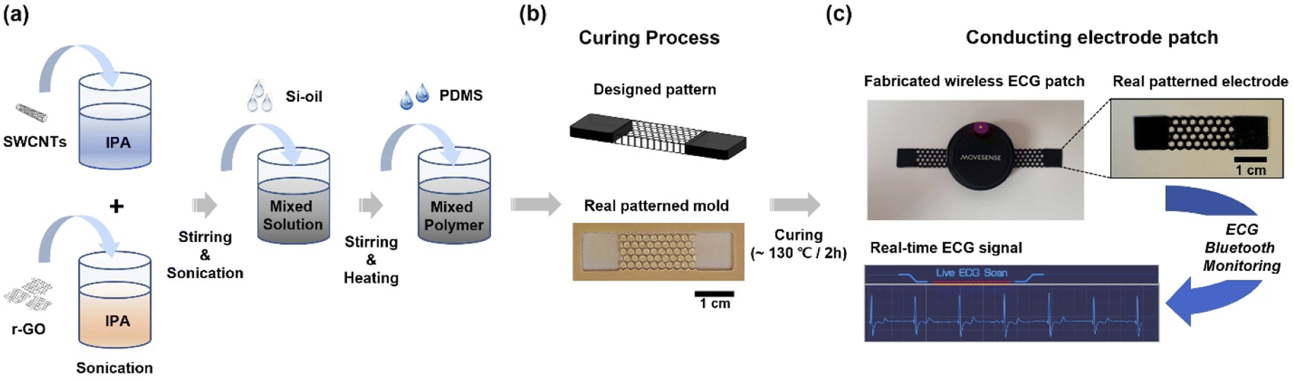 | ||
| Fig. 1 Schematic of stretchable conducting polymer nanocomposite electrode patch fabrication for ECG Bluetooth monitoring. | ||
Measurement and analysis of ECG signals
The Movesense sensor (MODEL:OP174), to which the MAX30003 chip was used to measure the ECG signal of the human body, was purchased from SUNNTO in Finland (Fig. S10†). The Movesense was combined with the nanocarbon-based polymer composite electrode fabricated in this study and attached to the body using a 3M Tegaderm™ film (1626W). The measured ECG signal data were transmitted via a Bluetooth system and collected by a sensor application developed using C# programming (Fig. S11†). The ECG signal was measured at 250 samples per second, and the received signal was used without any movement or amplification. A commercial Ag/AgCl gel electrode was purchased from (2223H, 3M), and after measurement and detection of the ECG signal under equal conditions, the results were compared and analyzed.
Characterisation
The morphologies of the PDMS, SWCNTs, r-GO, and nanocomposite films were observed using field-emission scanning electron microscopy (FE-SEM; MIRA-II TESCAN, Czech Republic). The Raman spectra (RM1000, Renishaw, UK) were obtained using an excitation laser with a wavelength of 514 nm. Attenuated total reflectance-Fourier transform infrared spectroscopy (ATR-FTIR) analysis was performed using an ALPHA-P spectrometer (Bruker, USA). The SWCNTs and r-GO powders were mixed with potassium bromide (KBr), compressed into pellets (thickness ∼3 mm), and analyzed in transmission mode using an FT-IR-microscope vacuum spectrometer system (Vertex 80v, Bruker, USA) within the range of 400–4000 cm−1. The chemical states of all the samples were analyzed through XPS (K-Alpha, Thermo Scientific, USA). XPS spectra were acquired with normal emission geometry using conventional monochromatic AlKα radiation (hν = 1486.6 eV) with a pass energy of 50 eV and an energy step of 0.1 eV. A flood gun was used as charge neutralizer. The C 1s peaks of all samples were set to 284.5 eV to calibrate the binding energy values.40–43 All the C 1s spectra were normalized by adjusting the maximum intensities of the C 1s spectra to 1.0. The electrical resistances of the fabricated conducting polymer nanocomposite films were measured using 2 and 4-point probe methods (Keithley 2400 source measurement unit) at room temperature and pressure. The wirelessly monitored ECG Bluetooth signals were analyzed via a self-developed tablet application (Fig. S10 and S11†) coupled with a commercial Movesense sensor module.Results and discussion
A PDMS-based nanocomposite film containing SWCNTs and r-GO as conductive nanofillers was prepared to fabricate flexible electrode patches for real-time ECG Bluetooth monitoring, as shown in Fig. 1. To fabricate a PDMS-based conductive electrode, SWCNTs and r-GO were dispersed in IPA solutions separately, stirred, and sonicated; next, Si-oil was added to improve the dispersibility. The suspension was mixed with a silicone elastomer (PDMS), and a filler/polymer mixture was fabricated using a prepatterned mold (Fig. 1a). Fig. 1b shows a conductive nanocomposite electrode (40 mm × 10 mm × 1 mm) fabricated using a vacuum-drying process. To evaluate the performance of the fabricated conductive electrodes, a pair of patterned electrodes was combined with an ECG sensing module for real-time ECG Bluetooth monitoring (Fig. 1c). The experimental procedures are described in detail in the experimental section. The pristine materials (PDMS, SWCNTs, and r-GO) and details of the fabricated conducting nanocomposite films are listed in Table 1. Three types of hybrid electrode materials were designed and used to fabricate nanocomposites with uniform and high conductivity. The first nanocomposite (P-SW; type I), based on PDMS-SWCNTs, contained only SWCNTs (2 wt%). The second nanocomposite (P-SW/r-GO; type II), based on PDMS-SWCNTs/r-GO, was composed of a hybrid structure of SWCNTs (1 wt%) and r-GO (1 wt%) for more conductive connection bridges than the conductive point contacts by the network junctions with only SWCNTs. The third nanocomposite (P-SW/r-GO/f; type III) was based on PDMS-SWCNTs/r-GO/fabric, containing a fabric layer (Fabric wiper, WW-2019, KM, Korea) for efficient vacuum degassing and curing. The PDMS-r-GO (2 wt%)-based nanocomposite film (Fig. S1†) was excluded as it exhibited small broken structures despite being fabricated by the process with fabrication conditions identical to those for other nanocomposites (Table S1†).Fig. 2 shows the digital photographs and FE-SEM images of the pristine samples and the polymer nanocomposite films. Fig. 2a and b show the characteristic morphologies of SWCNTs with randomly entangled bundle networks and r-GO with hierarchical structures of entangled flakes with sizes on the order of tens of micrometers. The P-SW exhibited a non-uniform and extremely rough surface (Fig. 2c). The surface morphologies of the additional polymer nanocomposite films with various amounts of SWCNTs (1–3 wt%) also exhibited similar surface characteristics (not shown here).
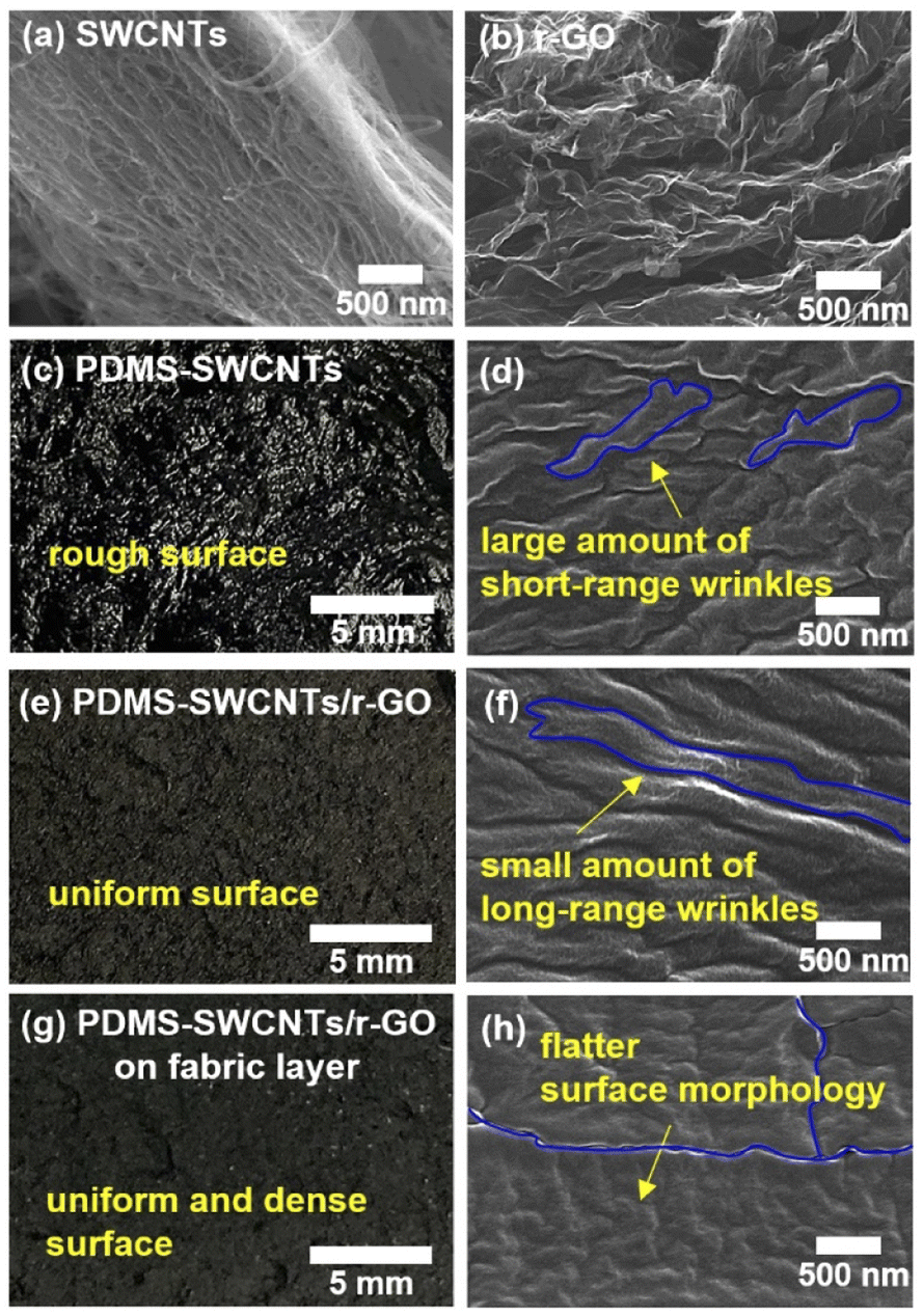 | ||
| Fig. 2 FE-SEM images of (a) SWCNTs and (b) r-GO. Digital photographs and FE-SEM images of the fabricated conducting nanocomposite films for (c and d) P-SW (PDMS-SWCNTs), (e and f) P-SW/r-GO (PDMS-SWCNTs/r-GO), and (g and h) P-SW/r-GO/f (PDMS-SWCNTs/r-GO on fabric layer). | ||
The non-uniformity and severe roughness could be attributed to the presence of several microbubbles that could not be removed during the vacuum degassing process owing to the strong bundling effect of the SWCNTs27,44 and the randomly entangled aggregate network structure. This phenomenon contrasts with the surface morphology of the large-diameter MWCNT-based conducting nanocomposite film, in which the bundling effect is absent. In the case of MWCNTs with a large diameter (>15 nm) and small aspect ratio (approximately 104), most of the bubbles escape easily, whereas in the case of SWCNTs with smaller diameters (∼1 nm) and larger aspect ratios (approximately 106), the bubbles are not easily removed despite long-term vacuum degassing.34–36 FE-SEM observation of the P-SW surface (Fig. 2d) revealed a morphology with numerous short-range wrinkles. This P-SW surface structure with severe roughness and short-range wrinkles could result in low electrical conductivity owing to its high contact resistance. This would hinder its application as an electrode for ECG monitoring, which requires close contact with the skin to achieve high electrical conductivity.
To improve the non-uniform network structure in the P-SW nanocomposite film caused by the large bundles and entangled structures of SWCNTs, a hybrid-type structure combining SWCNTs and r-GO with abundant conductive connection bridges was introduced. Fig. 2e shows a digital photograph of the P-SW/r-GO nanocomposite film. Unlike P-SW, P-SW/r-GO exhibited a relatively uniform matte surface. The FE-SEM images (Fig. 2f) also indicate that P-SW/r-GO had a more uniform surface morphology with long-range wrinkles and well-networked pathways than P-SW. These surface characteristics of uniform well-networked wrinkles can lead to a low and narrow resistance distribution. Fig. 2g shows a digital photograph of the P-SW/r-GO/f nanocomposite film, which reveals a uniform and dense surface structure. The fabric layer facilitated the removal of residual chemicals and air bubbles from the composite during curing. The corresponding FE-SEM images (Fig. 2h) reveal a flatter surface morphology, comprising long-range wrinkles, than that of P-SW/r-GO. The uniform dense surface (Fig. S2†) indicates that the hybrid structure combining SWCNTs and r-GO was highly crosslinked with silicone oligomers.
Fig. 3a shows the Raman spectra of the PDMS, SWCNTs, and r-GO. The Raman spectrum of PDMS exhibited several characteristic peaks of the silicone elastomer. Peaks corresponding to skeletal C–C bending vibrations and symmetric Si–O–Si stretching were detected at ∼150–300 cm−1 and ∼490 cm−1, respectively.45 In addition, strong intensity peaks corresponding to symmetric and antisymmetric –CH3 stretching vibrations were observed at ∼2896 and 2955 cm−1, respectively.45 In the SWCNT spectrum, peaks in a clear radial breathing mode (RBM) region with diameters of 1.37–1.67 nm, corresponding to 180–150 cm−1 (Fig. S3 and S4†); a D-band at ∼1343 cm−1, corresponding to graphite-like carbon vibrational modes, and a G-band at ∼1580 cm−1, corresponding to disordered carbon, were observed (Fig. 3a). The value of ID/IG for the SWCNTs was 0.01, implying high crystallinity. This value is similar to that of previously reported highly crystalline SWCNTs (ID/IG = 0.008) synthesized using the arc discharge method.27 Highly crystalline SWCNTs with such an extremely low ID/IG value could provide high electrical conductivity if an appropriate network assembly structure was introduced.46 The spectrum of r-GO also exhibited a G-band at ∼1567 cm−1 and a D-band at ∼1340 cm−1, indicating graphitic and disordered structures, respectively. In particular, the ID/IG and I2D/IG values for r-GO are 0.20 and 0.71, respectively, implying high crystallinity and a few-layer graphene structure.47,48
 | ||
| Fig. 3 Raman spectra of (a) PDMS, SWCNTs, and r-GO, and (b) P-SW, P-SW/r-GO, and P-SW/r-GO/f conducting nanocomposite films. | ||
Fig. 3b shows the Raman spectra of P-SW, P-SW/r-GO, and P-SW/r-GO/f nanocomposite films. The spectrum of P-SW exhibited weak peaks corresponding to the C–C, Si–O–Si, and –CH3 vibration modes of PDMS, along with the characteristic RBM region (Fig. S4†), D-band, G-band, and 2D band of the SWCNTs. Such antisymmetric –CH3 stretching vibrations with low intensities may be related to the relatively dominant SWCNT-bundle structure on the non-uniform surface or the severe roughness caused by partial phase separation between the SWCNTs and PDMS during vacuum degassing and curing of the SWCNT nanocomposite films, as shown in Fig. 2c. In addition, the ID/IG was 0.01, which was similar to that of the pristine SWCNTs. By contrast, the ID/IG of P-SW/r-GO and P-SW/r-GO/f increased slightly from 0.01 to ∼0.03 because of the mixing of SWCNTs and r-GO. The Si–O–Si, S–C, and –CH3 vibrational modes for P-SW/r-GO and P-SW/r-GO/f exhibited higher intensities and clearer Raman spectra than those of P-SW. The distinct appearance of various vibration modes in the Raman spectral change of the nanocomposite film suggests that the 2D r-GO (1 wt%) acted as a network bridge, forming an appropriate conducting pathway with 1D SWCNTs (1 wt%), and was well-dispersed inside the PDMS (98 wt%).
To determine whether the carbon-based nanomaterials were thoroughly mixed with PDMS, FTIR spectroscopy and X-ray photoelectron spectroscopy (XPS) were performed on the nanocomposite films. Fig. 4a shows the FTIR spectra of nanocomposite films with SWCNTs, r-GO, and PDMS. All nanocomposite films (P-SW, P-SW/r-GO, and P-SW/r-GO/f) showed absorption bands corresponding to Si–CH3 (∼1255 cm−1 and 680–850 cm−1), Si–O–Si and/or Si–O–C symmetric stretching (∼1000–1150 cm−1), C![[double bond, length as m-dash]](https://www.rsc.org/images/entities/char_e001.gif) O (∼1739 cm−1), and C–H stretching (CH3) (∼2963 cm−1), which are associated with the chemical bonds in PDMS.45–49 The peak at ∼1537 cm−1, assigned to the C–C bending vibration of carbon bonding, exhibited a low intensity because the amounts of SWCNTs (1 wt%) and r-GO (1 wt%) were negligible in relation to that of PDMS (98 wt%) (Fig. 4a and S5†). In particular, the Si–O–C symmetric stretching (near 1135 cm−1) is difficult to observe in the FTIR spectra because it overlaps with the Si–O–Si absorption band. This is discussed along with the Si 2p XP spectra shown in Fig. 4e.
O (∼1739 cm−1), and C–H stretching (CH3) (∼2963 cm−1), which are associated with the chemical bonds in PDMS.45–49 The peak at ∼1537 cm−1, assigned to the C–C bending vibration of carbon bonding, exhibited a low intensity because the amounts of SWCNTs (1 wt%) and r-GO (1 wt%) were negligible in relation to that of PDMS (98 wt%) (Fig. 4a and S5†). In particular, the Si–O–C symmetric stretching (near 1135 cm−1) is difficult to observe in the FTIR spectra because it overlaps with the Si–O–Si absorption band. This is discussed along with the Si 2p XP spectra shown in Fig. 4e.
 | ||
| Fig. 4 (a) FTIR spectra of PDMS, P-SW, P-SW/r-GO, and P-SW/r-GO/f. (b) XPS survey scan spectra of PDMS, SWCNTs, r-GO, P-SW, P-SW/r-GO, and P-SW/r-GO/f. C 1s (c and d) and Si 2p (e) XPS spectra of the pristine samples and nanocomposite films. | ||
Fig. 4b shows the XPS survey scan spectra used to analyze the surface chemical compositions of the nanocomposite films. PDMS consisted of oxygen (24.0 at.%), carbon (49.3 at%), and silicon (26.7 at%) (Table S2†). In contrast, SWCNTs and r-GO had a relatively small oxygen-to-carbon ratio (Table S2 and Fig. S6†). The differences in the elemental compositions of the fabricated nanocarbon-based composite conducting films (P-SW, P-SW/r-GO, and P-SW/r-GO/f) and PDMS are small because the amounts of added nanocarbons are much smaller than that of PDMS, and thus do not affect the overall elemental composition. However, chemical state analysis of the C 1s (Fig. 4c and d) and Si 2p (Fig. 4e) XPS spectra revealed three differences: a decrease in FWHM, a decrease in C–H features, and a shift in Si 2p peaks.
First, the FWHMs of the C 1s spectra of the SWCNTs and r-GO (Fig. 4c) were 0.954 and 1.181 eV, respectively, which are lower than that of PDMS, which has an FWHM of 1.722 eV (Table S3†). Hence, the nanocarbon-added conductive composite films (P-SW (1.720 eV), P-SW/r-GO (1.455 eV), and P-SW/r-GO/f (1.491 eV)) had a lower FWHM than PDMS. In the C 1s spectra of SWCNTs and r-GO, the peak at 291 eV originates from π–π* shaking and in that of PDMS, the peak at 283 eV originates from C–H bonding (Fig. 4c).50 In spite of the large amounts of PDMS in the fabricated nanocarbon-based conductive composite films (P-SW, P-SW/r-GO, and P-SW/r-GO/f), the peak originating from C–H bonding (near 292 eV) is decreased in the C 1s XPS spectra of P-SW, P-SW/r-GO, and P-SW/r-GO/f, indicating that Si–C–H bonding in PDMS is bonded with carbon in conductive nanocarbons such as SWCNTs and r-GO. This phenomenon was also confirmed by the Si 2p spectrum (Fig. 4e). In addition, the Si 2p peak positions of P-SW (102.5 eV), P-SW/r-GO (102.4 eV), and P-SW/r-GO/f (102.3 eV)were shifted to a lower binding energy compared to the peak position of PDMS (102.6 eV), as shown in Fig. 4e, which is attributed to the Si–O–C bond between the silicon oligomer and nanocarbon formed via the thermal curing process.51 These results indicate that the nanocarbon-based conductive composite films were quite uniformly fabricated.
Fig. 5a shows a schematic of the three types (P-SW, P-SW/r-GO, and P-SW/r-GO/f) introduced to improve the electrical resistivity of the conductive nanocomposites. The P-SW/r-GO/f indicates that the introduction of breathable fabric structures can form dense 1D and 2D conductive network structures through effective vacuum degassing and curing to form packed nanocomposites (Fig. S7†). To evaluate the resistance characteristics of the fabricated conductive nanocomposites, the resistance values obtained using the two-probe (Fig. 5b) and four-probe (Fig. S8†) methods were considered the contact resistance (Fig. 5c) and uniformity (R2w-contact uniformity, Fig. 5d) obtained from the difference between the contact resistances. Here, the contact resistance values used for the two-probe measurements were calculated by subtracting the resistance obtained using the four-point method (Fig. S8†) from the resistance obtained using the two-point method (Fig. 5c). P-SW exhibited an average resistance of 1871 Ω (Fig. 5b) and a very wide resistance distribution (783 Ω, Fig. 5d). This was attributed to its non-uniform network structure, with high roughness and numerous short-range wrinkles, as shown in Fig. 2c and d. P-SW/r-GO had an average resistance of 63 Ω (Fig. 5b) and a narrower resistance distribution (128 Ω in Fig. 5d), suggesting that the 2D r-GO nanoflakes were uniformly dispersed in the random 1D SWCNT network structure inside the PDMS matrix, creating a new tightly connected 1D + 2D conducting pathway in the nanocomposite film. In the case of P-SW/r-GO/f, a low resistance (R4W = 4 Ω in Fig. S8;†R2W = 15 Ω in Fig. 5b) and very narrow resistance distribution (7 Ω in Fig. 5d) were achieved. This is due to the use of the fabric layer, which facilitated the removal of residual chemicals and air bubbles in the composite during the curing process, which is consistent with the uniform and dense surface structure observed in Fig. 2g, h, and S2†.
 | ||
| Fig. 5 (a) Schematic of the fabricated conductive nanocomposite electrode. The inset shows that the introduction of a breathable fabric structure enables effective vacuum degassing and curing to form dense 1D and 2D conductive network structures to form packed nanocomposites. (b) 2-Probe resistance measurement characteristics, (c) contact resistance, and (d) resistance uniformity (R2w-contact uniformity) of P-SW, P-SW/r-GO, and P-SW/r-GO/f nanocomposite films obtained from the difference between contact resistances. | ||
The remarkable improvement in the electrical properties of the P-SW/r-GO/f nanocomposite is attributed to the following factors. First, prior to curing, the SWCNTs, r-GO, and Si-oil with appropriate viscosity, when mixed with the main polymer (i.e., PDMS), efficiently formed conducting pathways in the mixed interface through uniform dispersion. Second, introducing a breathable fabric structure enables effective vacuum degassing and curing, leading to densely accumulated 1D and 2D conductive network structures to form a packed nanocomposite (Fig. S7†). Controlling the network bridging of the mixed interface between the conductive nanomaterials in the polymer (i.e., PDMS) can reduce the contact resistance (Fig. 5c) of the nanocomposite and improve its uniformity (Fig. 5d). These results indicate that the formation of conducting network pathways and control of densely packed mixed interfaces play an important role in the fabrication of carbon-based nanocomposites hardened via crosslinking (Fig. S9†). By controlling the complex interface between the SWCNTs and r-GO, it is possible to reduce the contact resistance between the materials and fabricate conducting nanocomposite electrodes with high uniformity. Thus, the developed high-performance conducting nanocomposite has the potential to be used repeatedly as a wearable dry electrode.
ECG signals were measured using the fabricated conductive polymer nanocomposite as an electrode. Fig. 6a shows digital photographs of a wireless Bluetooth module and dry ECG electrodes attached to human skin for real-time ECG monitoring. In addition, it shows the ECG signal measured in real time using a self-developed tablet application (See Movie S1†). A pair of fabricated electrodes (Fig. 1c) was coupled to a commercially available sensor module (Fig. S10†) for continuous ECG monitoring. ECG signals were collected wirelessly through the aforementioned tablet application (Fig. S11†) and analyzed. In order to ensure the stability and accuracy of the ECG signal, the experiment was performed and confirmed over dozens of iterations for all nanocomposite electrodes. Fig. 6b–e compare the ECG signals measured using a commercial Ag/AgCl gel electrode and dry-type conductive electrodes fabricated using P-SW, P-SW/r-GO, and P-SW/r-GO/f. Although the ECG signal measured using the P-SW electrode exhibited a basic R and S-wave signal shape, a significant amount of noise made it difficult to distinguish between the P and T waves (Fig. 6c). This is consistent with the rough and non-uniform surface characteristics owing to SWCNT aggregation and the wide resistance distribution of the composite electrode (Fig. 2c–d and 5a–c).
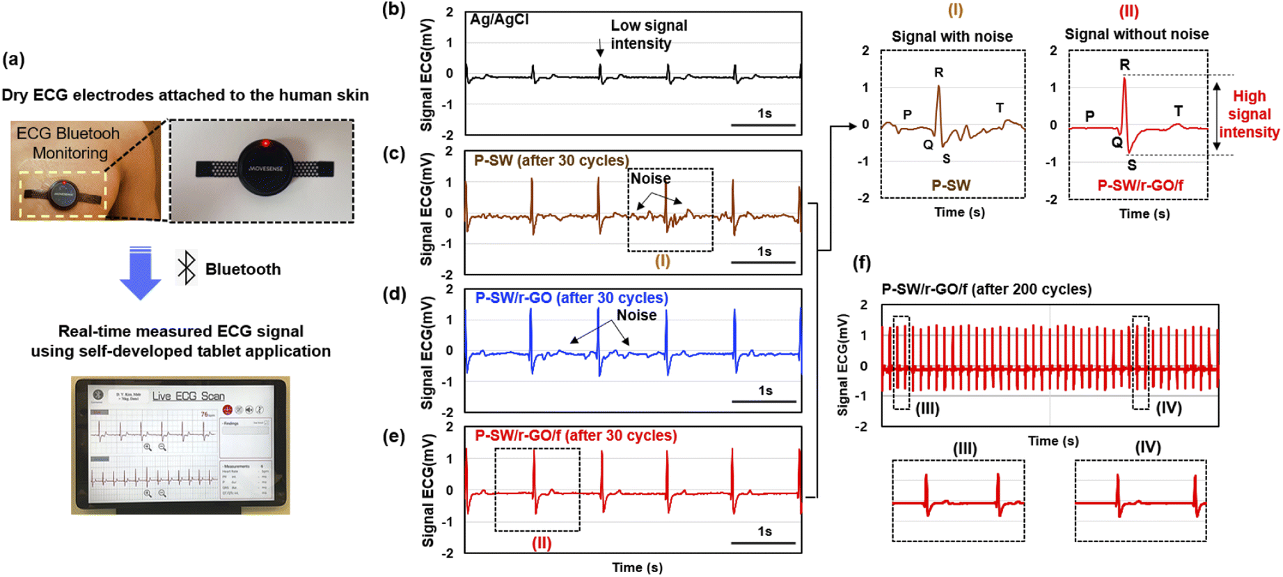 | ||
| Fig. 6 (a) Schematic of dry ECG electrodes attached to the body for wireless ECG monitoring. Comparison of ECG signals measured using (b) commercial Ag/AgCl gel electrode and dry conducting nanocomposite electrodes for (c) P-SW, (d) P-SW/r-GO, (e) P-SW/r-GO/f, and (f) P-SW/r-GO/f tested after 200 cycles. | ||
For P-SW/r-GO (Fig. 6d), the noise was slightly reduced in the P and T wave regions, and the response signal was similar to that obtained using the Ag/AgCl gel electrode. This exemplifies the uniform surface characteristics of P-SW/r-GO and is consistent with the narrower resistance distribution of P-SW/r-GO caused by the well-developed long conducting pathways resulting from the formation of long-range wrinkles (Fig. 2e–f and 5a–c). An even clearer ECG signal with high intensity was obtained using the P-SW/r-GO/f electrode; this signal had well-defined P, Q, R, S, and T waves and was devoid of noise (Fig. 6e). This can be attributed to the considerably narrower resistance distribution of P-SW/r-GO/f, stemming from the formation of well-developed long and large-range wrinkles and the exceedingly low contact resistance (Fig. 2g–h and 5a–c). Thus, simple, repeatable, and cost-effective electrodes based on a complex interface assembly with well-developed conducting pathways can be fabricated and used for accurate and convenient wireless healthcare monitoring and future wearable electronics.
Conclusions
Three types of PDMS-based flexible nanocomposite films incorporating high-conductivity 1D SWCNTs and 2D r-GO were fabricated; their properties were compared to verify their applicability in high-performance wearable ECG electrodes. First, the P-SW nanocomposite based on PDMS-SWCNTs exhibited a rough and non-uniform surface morphology owing to the strong bundling effect of the raw SWCNTs, randomly entangled aggregate structures, and imperfect vacuum degassing. This surface characteristic is the primary cause of the high contact resistance (1871 Ω) of the P-SW nanocomposite. The P-SW/r-GO nanocomposite, with a hybrid structure combining SWCNTs and r-GO, showed uniform surface characteristics and, consequently, a low contact resistance (63 Ω) owing to the formation of hybrid and short conducting pathways. Finally, the P-SW/r-GO/f nanocomposite, with a fabric-assisted structure that enabled efficient vacuum degassing and curing, exhibited long and wide conducting pathways in a more uniform and denser interconnected structure. The fabricated electrodes using the optimized nanocomposites performed the same (i.e., P-SW/r-GO) or higher (i.e., P-SW/r-GO/f) than a commercial wet-type Ag/AgCl gel electrode during real-time measurement for ECG wireless monitoring. Consequently, the resistance of P-SW/r-GO/f electrode is substantially reduced to 15 Ω. Moreover, no change in the performance or structure was observed despite repeated usage (Fig. 6f). The nanocarbon-based high-performance hybrid conductive polymer composite electrodes developed in this study can be effectively applied in future wearable electronic devices and wireless personal health monitoring systems, facilitating easy and accurate measurements regardless of time and place.Author contributions
D. Y. K: conceptualization, methodology, investigation, writing: original draft, review and editing. G. L: methodology, investigation, data analysis. G. Y. L and J. K: methodology, data analysis. K. J: conceptualization, methodology. K. S. K: conceptualization, methodology, investigation, writing: review and editing, supervision, project administration, funding acquisition.Conflicts of interest
There are no conflicts to declare.Acknowledgements
This work was supported by the National Research Foundation of Korea (NRF) grant, funded by the Korea government (MSIT) (No. 2019R1A2C1009963). This research supported by Global Research Development Center Program (No. 2018K1A4A3A01064272) and Basic Science Research Program (No. 2021R1A4A1031900) through the National Research Foundation of Korea (NRF) funded by the Ministry of Science and ICT (MSIT). And also this work was supported by the Technology Innovation Program (20017548) funded by the Ministry of Trade, Industry & Energy (MOTIE, Korea).References
- N. Matsuhisa, M. Kaltenbrunner, T. Yokota, H. Jinno, K. Kuribara, T. Sekitani and T. Someya, Nat. Commun., 2015, 6, 7461 CrossRef CAS PubMed.
- S. Yao and Y. Zhu, Adv. Mater., 2015, 27, 1480–1511 CrossRef CAS PubMed.
- J. Kim, D. Son, M. Lee, C. Song, J.-K. Song, J. H. Koo, D. J. Lee, H. J. Shim, J. H. Kim, M. Lee, T. Hyeon and D.-H. Kim, Sci. Adv., 2016, 2, e1501101 CrossRef PubMed.
- J. Kim, A. S. Campbell, B. E.-F. d. Ávila and J. Wang, Nat. Biotechnol., 2019, 37, 389–406 CrossRef CAS PubMed.
- D. Pani, A. Achilli and A. Bonfiglio, Adv. Mater. Technol., 2018, 3, 1800008 CrossRef.
- T. Roberts, J. B. D. Graaf, C. Nicol, T. Hervé, M. Fiocchi and S. Sanaur, Adv. Healthcare Mater., 2016, 5, 1462–1470 CrossRef CAS PubMed.
- S. Debener, R. Emkes, M. De Vos and M. Bleichner, Sci. Rep., 2015, 5, 16743 CrossRef CAS PubMed.
- M. Mahmood, D. Mzurikwao, Y.-S. Kim, Y. Lee, S. Mishra, R. Herbert, A. Duarte, C. S. Ang and W.-H. Yeo, Nat. Mach. Intell., 2019, 1, 412–422 CrossRef.
- W. Honda, S. Harada, T. Arie, S. Akita and K. Takei, Adv. Funct. Mater., 2014, 24, 3299–3304 CrossRef CAS.
- G. A. Mensah, G. S. Wei, P. D. Sorlie, L. J. Fine, Y. Rosenberg, P. G. Kaufmann, M. E. Mussolino, L. L. Hsu, E. Addou, M. M. Engelgau and D. Gordon, Circ. Res., 2017, 120, 366–380 CrossRef CAS PubMed.
- B. Liu, Z. Luo, W. Zhang, Q. Tu and X. Jin, Sens. Actuators, A, 2016, 247, 459–464 CrossRef CAS.
- H.-L. Peng, J.-Q. Liu, H.-C. Tian, B. Xu, Y.-Z. Dong, B. Yang, X. Chen and C.-S. Yang, Sens. Actuators, A, 2015, 235, 48–56 CrossRef CAS.
- S. Yao and Y. Zhu, JOM, 2016, 68, 1145–1155 CrossRef.
- Y. Gu, T. Zhang, H. Chen, F. Wang, Y. Pu, C. Gao and S. Li, Nanoscale Res. Lett., 2019, 14, 263 CrossRef.
- H. Jin, Y. S. Abu-Raya and H. Haick, Adv. Healthcare Mater., 2017, 6, 1700024 CrossRef PubMed.
- L. Zhang, K. S. Kumar, H. He, C. J. Cai, X. He, H. Gao, S. Yue, C. Li, R. C.-S. Seet, H. Ren and J. Ouyang, Nat. Commun., 2020, 11, 4683 CrossRef CAS PubMed.
- F. Stauffer, M. Thielen, C. Sauter, S. Chardonnens, S. Bachmann, K. Tybrandt, C. Peters, C. Hierold and J. Vörös, Adv. Healthcare Mater., 2018, 7, 1700994 CrossRef PubMed.
- F. Sana, E. M. Isselbacher, J. P. Singh, E. K. Heist, B. Pathik and A. A. Armoundas, J. Am. Coll. Cardiol., 2020, 75, 1582–1592 CrossRef.
- M. Zulqarnain, S. Stanzione, G. Rathinavel, S. Smout, M. Willegems, K. Myny and E. Cantatore, npj Flexible Electron., 2020, 4, 13 CrossRef.
- M. Xu, D. N. Futaba, T. Yamada, M. Yumura and K. Hata, Science, 2010, 330, 1364–1368 CrossRef CAS PubMed.
- D. Y. Kim, H. Sugime, K. Hasegawa, T. Osawa and S. Noda, Carbon, 2011, 49, 1972–1979 CrossRef CAS.
- D. Y. Kim, H. Sugime, K. Hasegawa, T. Osawa and S. Noda, Carbon, 2012, 50, 1538–1545 CrossRef CAS.
- K. S. Kim, Z. Yue, H. Jang, S. Y. Lee, J. M. Kim, K. S. Kim, J.-H. Ahn, P. Kim, J.-Y. Choi and B. H. Hong, Nature, 2009, 457, 706–710 CrossRef CAS.
- K. P. Hong, K. H. Lee, J. Nam, K.-S. Kim, S. H. Kim, B. Kim, K. Kim, J. S. Park, J. Y. Lee, T. Jeong, Y. J. Song, J.-Y. Hwang, J. B. Choi, S. Cho, K. S. Kim and H. K. Kim, Appl. Surf. Sci., 2019, 496, 143614 CrossRef CAS.
- W. Zhao and S. Xu, Nanoscale Adv., 2022, 4, 250–257 RSC.
- S. J. Kim, D. H. Shin, Y. S. Choi, H. Rho, M. Park, B. J. Moon, Y. Kim, S.-K. Lee, D. S. Lee, T.-W. Kim, S. H. Lee, K. S. Kim, B. H. Hong and S. K. Bae, ACS Nano, 2018, 12, 2803–2808 CrossRef CAS PubMed.
- D. Y. Kim, C.-M. Yang, H. Noguchi, M. Yamamoto, T. Ohba, H. Kanoh and K. Kaneko, Carbon, 2008, 46(4), 611–617 CrossRef CAS.
- D. Y. Kim, K. S. Kim, C.-M. Yang and J. Kim, ACS Omega, 2021, 6, 7015–7022 CrossRef CAS PubMed.
- D. Y. Kim, J. H. Kim, M. Li, S. Noda, J. Kim, K.-S. Kim, K. S. Kim and C.-M. Yang, Appl. Surf. Sci., 2021, 566, 150751 CrossRef CAS.
- J. Foroughi and G. Spinks, Nanoscale Adv., 2019, 1, 4592–4614 RSC.
- A. Kolanowska, A. P. Herman, R. G. Jędrysiak and S. Boncel, RSC Adv., 2021, 11, 3020–3042 RSC.
- J. Jung, S. Shin and Y. T. Kim, Microelectron. Eng., 2019, 203–204, 25–30 CrossRef CAS.
- E. P. Gilshteyn, S. Lin, V. A. Kondrashov, D. S. Kopylova, A. P. Tsapenko, A. S. Anisimov, A. J. Hart, X. Zhao and A. G. Nasibulin, ACS Appl. Mater. Interfaces, 2018, 10(33), 28069–28075 CrossRef CAS PubMed.
- B. Liu, H. Tang, Z. Luo, W. Zhang, Q. Tu and X. Jin, Actuators, A, 2017, 265, 79–85 CrossRef CAS.
- J. H. Kim, J.-Y. Hwang, H. R. Hwang, H. S. Kim, J. H. Lee, J.-W. Seo, U. S. Shin and S.-H. Lee, Sci. Rep., 2018, 8, 1375 CrossRef PubMed.
- Q. Chen, Y. Li, D. Xiang, Y. Zheng, W. Zhu, C. Zhao, H. Li, H. Han and Y. Shen, Macromol. Mater. Eng., 2020, 305, 1900525 CrossRef CAS.
- J.-W. Lee and K.-S. Yun, Polymers, 2017, 9, 439 CrossRef PubMed.
- F. J. Romero, E. Castillo, A. Rivadeneyra, A. Toral-Lopez, M. Becherer, F. G. Ruiz, N. Rodriguez and D. P. Morales, npj Flexible Electron., 2019, 3, 12 CrossRef.
- M. A. Zahed, P. S. Das, P. Maharjan, S. C. Barman, M. Sharifuzzaman, S. H. Yoon and J. Y. Park, Carbon, 2020, 15, 26–36 CrossRef.
- G. Lee, D. W. Jung, W. Lee, S. Nah, S. Ji, J. Y. Hwang, S. S. Lee, S. Park, S. S. Chae and J.-O. Lee, Carbon, 2019, 141, 774–781 CrossRef CAS.
- J. Kim, Y. Yamada, Y. Suzuki, J. Ciston and S. Sato, J. Phys. Chem. C, 2014, 118, 7076–7084 CrossRef CAS.
- Y. Yamada, H. Yasuda, K. Murota, M. Nakamura, T. Sodesawa and S. Sato, J. Mater. Sci., 2013, 48, 8171–8198 CrossRef CAS.
- J. Kim, N. Lee, Y. H. Min, S. Noh, N.-K. Kim, S. Jung, M. Joo and Y. Yamada, ACS Omega, 2018, 3(12), 17789–17796 CrossRef CAS.
- C.-M. Yang, D. Y. Kim and Y. H. Lee, Chem. Mater., 2005, 17(25), 6422–6429 CrossRef CAS.
- A. N. Parvez, M. H. Rahaman, H. C. Kim and K. K. Ahn, Composites, Part B, 2019, 174, 106923 CrossRef CAS.
- Y. S. Song, C. M. Yang, D. Y. Kim, H. Kanoh and K. Kaneko, J. Colloid Interface Sci., 2008, 318, 365–371 CrossRef CAS PubMed.
- C.-H. Chen, S.-W. Yang, M.-C. Chuang, W.-Y. Woon and C.-Y. Su, Nanoscale, 2015, 7, 15362–15373 RSC.
- Y. Liu, Z. Liu, W. S. Lew and Q. J. Wang, Nanoscale Res. Lett., 2013, 8, 335 CrossRef.
- S. Song, Y. Zhai and Y. Zhang, ACS Appl. Mater. Interfaces, 2016, 8, 31264–31272 CrossRef CAS PubMed.
- D. Son, S. Cho, J. Nam, H. Lee and M. Kim, Polymers, 2020, 12, 1053 CrossRef CAS PubMed.
- S. Zeng, W. Feng, S. Peng, Z. Teng, C. Chen, H. Zhang and S. Peng, RSC Adv., 2019, 9, 30685–30692 RSC.
Footnotes |
| † Electronic supplementary information (ESI) available. See https://doi.org/10.1039/d2na00220e |
| ‡ These authors contributed equally. |
| This journal is © The Royal Society of Chemistry 2022 |