 Open Access Article
Photoconductivity of PbS/perovskite quantum dots in gold nanogaps†
Dario
Grimaldi
 *a,
Emil
Kelderer
a,
Dmitry N.
Dirin
 bc,
Maksym V.
Kovalenko
 bc,
Andreas
Hohenau
a,
Harald
Ditlbacher
a and
Joachim R.
Krenn
 a
a
aInstitute of Physics, University of Graz, 8010 Graz, Austria. E-mail: dario.grimaldi@uni-graz.at
bInstitute of Inorganic Chemistry, Department of Chemistry and Applied Biosciences, ETH Zürich, 8093 Zürich, Switzerland
cEmpa – Swiss Federal Laboratories for Materials Science and Technology, Laboratory for Thin Films and Photovoltaics, 8600 Dübendorf, Switzerland
First published on 18th July 2022
Abstract
We demonstrate that the photoconductance of colloidal PbS/MAPbI3 quantum dots in nanoscale gold electrode gaps shows a consistent power law dependence of the photocurrent on the light intensity with an exponent slightly below 0.7. The gap sizes are between 25 and 800 nm and by scanning photocurrent microscopy we evidence the strong localization and high reproducibility of photocurrent generation. We probe different flat-faced and pointed electrodes for excitation light in the red and near infrared spectral range and laser irradiances from 10−2 to 102 W cm−2. Our material combination provides practically identical photocurrent response for a wide range of gap sizes and geometries, highlighting its generic potential for nanoscale light coupling and detection.
1 Introduction
Miniaturizing active components to match the sub-micrometer dimensions of high-index waveguides, near field (e.g. plasmonic) structures or electronic components is a longterm challenge in photonics. Nanometer-sized colloidal semiconductor crystals (quantum dots, QDs) are an appealing choice in this context, being easily processable on a variety of substrates, including conventional semiconductor platforms. QDs are size-tunable in their quantized energy levels, they are strongly absorbing and show high quantum efficiencies.1 Thin films of closely packed QDs are efficient photoconductors, i.e. they increase their conductivity due to carrier generation upon the absorption of light, a property that was intensely investigated due to its relevance for light detectors and photovoltaics. In particular, QD detectors have shown record spectral ranges and sensitivities and due to charge trapping quantum efficiencies well above unity can be achieved.2,3When combined with sub-micrometer spaced metal electrodes, photoconductive QDs form nanoscale light detectors. For CdSe/ZnS QDs between gold electrodes just a few nm apart, responsivities of a few tens of mA W−1 (ref. 4) and light detection sensitivities of 500 fW (ref. 5) were reported. Crosstalk between close electrodes was found to be suppressed due to the strongly confined electric fields in nanoscale gaps.6 Understanding the role of charge trap population7 and related memory effects8 contributed to the reproducibility of photocurrent generation in nanogaps. Gaps a few nm wide that are bridged by just one QD (but by many in parallel) were realized, showing sub-microsecond photocurrent response.9
The dynamics of photogenerated carriers is encoded in the photocurrent dependence on the exciton generation rate that is proportional to the level of light irradiance. In principle, a linear dependence of the photocurrent as a function of irradiance is expected for a large number of available charge traps, corresponding to one type of charge carrier (electron or hole) being trapped and the photoconductive gain being given by the ratio of trap time and transit time of the circulating carrier (monomolecular recombination). This usually applies for low irradiances, when just a fraction of available charge traps is filled. In contrast, a square-root-dependence (or bimolecular recombination) is expected for a low number of available charge traps (or high irradiances, when most trap centers are filled). Often, however, different exponents α in the power-law-dependence, photocurrent ∝ irradianceα are observed. Although theoretical descriptions of photoconductance exist for many decades,10,11 the complex interplay of different trap types and the actual dynamics of carrier generation, transport and recombination makes it usually difficult to untangle the relative contributions. Exemplarily, power exponents of 1 and 0.5 were observed for lead-halide perovskite films for low and high irradiance, respectively.12 For CdSe/ZnS QDs in nano- and microgaps, low-temperature measurements yielded an exponent of 1,7,13 while for room temperature a value of 0.8 was found.7 A similar value was observed for a ZnO nanowire upon UV illumination,14 while it was 0.45 for Mn doped ZnO nanowires under blue light illumination.15 PbS films showed exponents between 0.45–0.68, dependent on the fabrication process of the electrode/QD system.16
Within the wide choice of QD materials, perovskite-capped PbS received a lot of recent attention, as the size-tunable IR absorption of PbS QDs combines favorably with organometal halide perovskite shells as MAPbI3 (ref. 17–21) for, first, further tunability of light absorption and emission.17,20,21 Second, with a view on photoconductance, perovskite shells of only about 1 nm thickness allow efficient charge transport between individual QDs in closely packed ensembles thereof.18,19,21
In this Letter, we investigate PbS/MAPbI3 QDs in nanoscale gaps defined by gold electrodes of varied geometries with mutual distances between 25 and 800 nm. For all sizes and different electrode geometries we observe quite similar power exponents of 0.60–0.69. We do not aim to untangle the detailed processes underlying the charge dynamics due to its multifaceted phenomenology. Rather, we show that the photocurrent response of our system is independent of electrode size and geometry. Therefore we image the QD-gaps by scanning photocurrent microscopy (SPCM), evidencing reproducible localized charge generation. We further evidence smallest detectable light levels around 100 fW (at 0.5 V bias) and deduce from our measurements maximum responsivities around 0.2 A W−1. As a reproducible, stable and sensitive system, PbS/MAPbI3 QDs in nanoscale gaps seem thus solid components in the context of nanoscale photodetection, optical switching and specific imaging applications.
2 Experimental
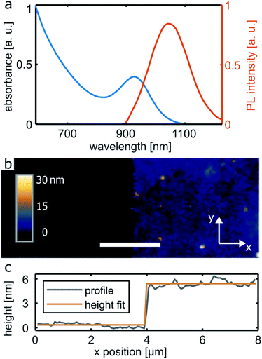
We fabricated gold electrodes with gap spacings between 25 and 800 nm (±5 nm) and either flat or pointed (bow tie) geometries. By electron beam lithography, the electrode patterns were exposed in a poly(methyl methacrylate) resist layer on glass. After chemical development, a 3 nm thick chromium adhesion layer and a 30 nm thick gold layer were added by physical vapor deposition. Resist and excess metal were finally removed by chemical lift-off (see Methods for further details). The electric contact lines to the gaps are built in the same lithographic step, extending over a length of 500 μm. Their corresponding widths depend on gap geometry and range from a few μm to about 40 nm in the case of the nanoscale bow tie structures. The ends of the contact lines were in turn overlaid by millimeter-sized gold pads by shadow mask evaporation for contacting with metal pins to interface with the measurement circuitry. Applied bias voltages were in the range 0.01–10 V, photocurrents were measured with a transimpedance amplifier at 1010 or 1011 gain and rise/fall times of 50 or 300 μs, respectively. The measured photocurrents were typically in the pA range, with dark currents smaller than 5% of the photocurrent value.3.1 nm large PbS colloidal QDs capped with lead oleate ligands were synthesized as described elsewhere.22,23 The procedure for phase transfer ligand exchange was adapted from our previous work.17 For all details, see the Methods section. Absorption and photoluminescence spectra of a QD solution (before ligand exchange) in 2,6-difluoropyridin are depicted in Fig. 1a. The PbS QD bandgap is size-dependent, the perovskite bandgap for MAPbI3 is at 1.63 eV (760 nm).24 The relative energy level values and thus the charge dynamics at the interface depends on the PbS QD size. The used PbS QDs display n-type transport behavior.25
The QDs were deposited on the electrodes by spin coating a 10 mg mL−1 solution in 2,6-difluoropyridin at 2000 rpm. The resulting films are 5.1 ± 0.4 nm thick (corresponding to a QD monolayer), as measured by atomic force microscopy (AFM) on a mechanically induced scratch, see Fig. 1b. As evidenced by AFM and scanning electron microscopy (SEM), the QD films are rather homogeneous, with a few randomly distributed QD agglomerations of 15–150 nm in diameter at μm separation distances.
As a powerful tool to image the spatial distribution of photocarrier generation and transport, scanning photocurrent microscopy (SPCM) relies on a focused laser beam that is scanned over an photoconductive sample, assigning the measured photocurrent to the respective laser position. This is in particular important for samples built from nanostructures, as it allows to assess the homogeneity of samples and to identify defects in the QD coverage. As shown in studies on CdSe/CdS QDs within μm-spaced electrodes, charge mobilities and transport pathways can be derived from SPCM measurements as well as local variations in light coupling to the sample.26,27 In our SPCM setup, we used a microscope objective with 40× magnification and 0.6 numerical aperture and a piezo stage for sample scanning. In parallel to the photocurrent measurement, an optical transmission image of the sample is acquired via a photodiode positioned behind the sample. For excitation, we used a supercontinuum laser emitting 6 ps pulses at 40 MHz repetition rate. Most experiments were done at an excitation wavelength of 650 nm, with further measurements at wavelengths at 600, 750 and 800 nm. In any case, the spectral bandwidth was 2.5 nm, selected by a volume holographic grating filter. For measuring the power dependence of the photocurrent, power levels in the nW to μW range were applied, corresponding to light irradiances between 10−2 and 102 W cm−2. The focus size was close to diffraction limited, as verified with measuring 1/e2 intensity value of a focused spot at 650 nm wavelength at a radius of 1.4 μm, by monitoring the transmitted light intensity when scanning over the sharp edge of an opaque metal film. This is confirmed by the lateral profile of photocurrent maps taken from nanoscale gaps. All SPCM measurements were done with a power of about 0.5 μW and an irradiance around 15 W cm−2.
3 Results and discussion
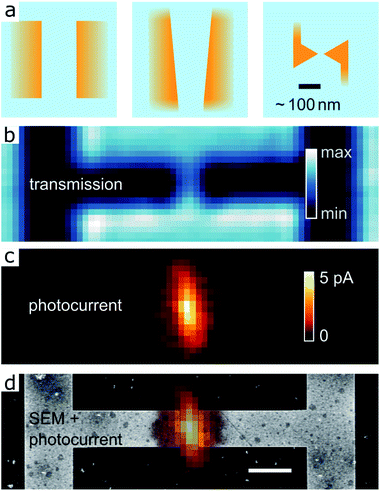
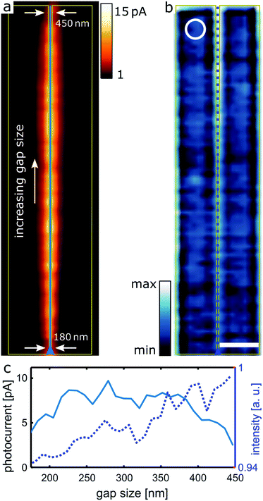
Sketches of the investigated electrode geometries are depicted in Fig. 2a. Largest gap sizes are 800 nm, while the smallest gaps measuring 25 nm are defined by a bow tie geometry. Individual gaps vary with ±5 nm, actual values are given where the respective measurements are discussed. For the ease of fabrication, the QDs are spun over the whole sample and thus cover the whole substrate surface. As we find in any case by SPCM, the photocurrents are only generated when the exciting laser is positioned well within the gap region, which we attribute to the strong field localization generated by the electrodes and the correspondingly localized photocurrents.4,7 This is evidenced exemplarily for an 800 nm gap defined by electrodes with parallel edges 1500 nm wide, as visible in the transmission image in Fig. 2b. The SPCM image (at 0.1 V bias voltage) in Fig. 2c and its overlay with a SEM image (Fig. 2d, SEM taken after the SPCM measurement) illustrate the localized photocurrent generation, any apparent delocalization is compatible with the focus size.The SPCM image of an electrode structure with a gap of varying size from 120 to 450 nm between two extended electrodes is shown in Fig. 3a. For this sample, the SPCM image shows a rather constant photocurrent along most of the slit, well confined to the gap region. The transmission image (Fig. 3b) and the corresponding cross-cut (Fig. 3c) shows that the transmission through the slit increases linearly with its size. The external quantum efficiency, which accounts for the variation of the absorptive cross section with the gap size, is shown in Fig. S1.† Gap-size-related resonance effects are thus not observed here.
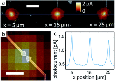
We next turn to nanoscale gaps defined by bow tie geometries with a gap size of 25 ± 5 nm. In Fig. 4a, a SPCM image of three bow tie gaps is shown, overlaid to a SEM image. For all gaps we observe quite similar signals, highlighted by the cross section in Fig. 4c. The photocurrent generation is well restricted to a region that corresponds to the focus size,4,7 as further evidenced by the high magnification image in Fig. 4a. We emphasize that a 25 nm wide gap is bridged by a QD film that contains only five QDs between the electrode tips. While apart from the example in Fig. 4 very similar photocurrent levels have been observed for about ten further gaps we conclude that our fabrication procedure yields very homogeneous QD films with rather similar QD numbers also in very small gaps. In contrast, for non-optimized film fabrication (drop casting instead of spin coating, different QD solution concentrations) we observed as well QD multilayers or agglomerates in individual gaps, that led to strongly varying photocurrents. In addition, we hypothesize that the complete absence of photocurrent signals observed for three gaps is due to a highly localized void in the QD film, as discussed in the ESI (Fig. S2†).
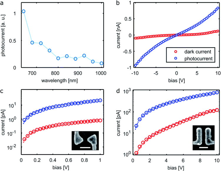
We now characterize the photoconductive properties of our QD/gap structures more closely. For a bow-tie gap (gap size 40 nm), we plot in Fig. 5a the wavelength dependence of the photocurrent (for the correction of the chromatic aberration of the microscope objective see the Methods section). Besides the evident increase towards lower wavelength, we find a rather weak but clear signature above a wavelength of 900 nm, corresponding well to the lowest energy QD absorbance (Fig. 1a), evidencing QD absorption as the initial step in photocurrent generation.
For a flat gap with 40 nm size and 200 nm width, the bias voltage dependence of the photocurrent is plotted in Fig. 5b. We note that the bias voltages used here, up to 10 V, are significantly higher than used for the other experiments in this work, that operate within the rather linear current regime up to 1 V. From the I/V curve around zero bias we can estimate the contact resistance of the QDs to the gold, which is around 20 MΩ. The same data on a logarithmic scale are plotted in Fig. 5d. Fig. 5c shows the corresponding I/V curves for a bow-tie gap (40 nm size). In any case, the red curve depicts the dark current, the blue curve depicts the photocurrent.
The photocurrent can be phenomenologically described by28
 | (1) |
The characteristic voltage barrier V0 and the equivalent sheet resistance R0 are about 5 V and 60 GΩ for the bow-tie gap and about 22 V and 10 GΩ for the flat gap, respectively. The average voltage drop per QD is thus 0.6 and 2.8 V, respectively, assuming a QD size of 5 nm. The high sheet resistance is to be expected for nanoscale electrodes, as compared to values in the MΩ range reported for laterally extended (interdigitated) electrodes.26 Interestingly, the phenomenological model of the fit describes the data from the ultrasmall gaps very well, while the concept of sheet resistance has been suggested to fail when only a few QDs are bridging a gap.26
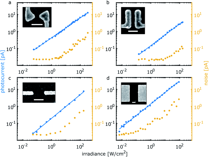
The dependence of the photocurrent on the exciting light irradiance was measured for different gap geometries, as summarized in Fig. 6 (blue symbols), the gaps are depicted in the inset SEM images. The exciting light wavelength was 650 nm in all cases. All data can be very well described by a power law with rather similar exponents α ranging from 0.60 to 0.69. The irradiance dependence of the photocurrent is largely independent on wavelength and bias, as illustrated in the ESI (Fig. S3 and S4†). While untangling the multitude of factors that could contribute to this specific value of the power law exponent (with respect to the excitation, dissociation transport and recombination dynamics of the charge carriers) is beyond the scope of this paper, a likely significant contribution is a combination of mono- and bimolecular recombination. This is in fact to be expected for different electron and hole mobilities,27 due to a resulting space charge layer giving rise to an exponent value of 0.75.29 In addition, some role might be played by (fluctuating) percolation paths in our quasi-2D QD monolayer samples, giving rise to a nontrivial charge transport dynamics.30,31
The lowest photocurrent value measured for an irradiance of 6 mW cm−2 at 650 nm wavelength was about 20 fA (for a bias voltage of 0.5 V). The responsivity for the bow-tie gaps, taking the actual focus and gap sizes into account yields normalized values around 0.2 A W−1. We note that we observed photocurrents as well at zero bias voltage, as depicted in the ESI (Fig. S5 and S6†).
Besides the photocurrent, we plot in Fig. 6 the corresponding noise (yellow symbols). The noise level is defined by the standard deviation of the static photocurrent, which is measured for five seconds for each irradiance value. For low irradiance levels noise is constant around 20 fA, to increase in proportion to the photocurrent for higher irradiances. On one hand, this can be due to fluctuating fields and conduction paths (transport noise), to be expected for nanoscale structures. On the other hand, charge generation and recombination noise that increases with irradiance can contribute.
4 Conclusion
We have shown that reproducible and stable nanoscale photoconductors in the red and near infrared spectral region can be fabricated with flat gold electrodes and PbS/MAPbI3 QDs. For gaps with sizes of 25–800 nm and either flat or pointed geometries, a power exponent around 0.60–0.69 was found for the irradiance dependence of the photocurrent over four orders of magnitude of light power. Importantly, nanoscale gaps enable the local measurement of light and/or light/matter coupling, as opposed to, e.g., interdigitated electrodes that average over large areas. Given existing fabrication processes,9 even gaps with just are few nm across that host a single QD seem feasible. Those would not only realize the ultimate limit in the miniaturization of QD photodetection, but as well bring elementary processes in QDs within experimental reach, e.g., single QD photocurrent and photoluminescence and the correlation of these two processes.12 Finally, optical functionality in the electrodes could further enrich the fundamental and applied aspects involved, in particular by exploiting plasmonic resonances of the electrodes.325 Methods
Electron beam lithography
For lithographic fabrication, we applied the beam of a scanning electron microscope to expose the electrode geometries in a 100 nm thick poly(methylmethacrylate) (PMMA) resist film on a cover slide glass substrate. An additional 60 nm thick layer of a conductive polymer (Allresist, AR-PC 5090) provided electric conductivity to prevent charging. After exposure, removal of the water-soluble conductive polymer layer and chemical development of the PMMA mask, we deposited a 3 nm thick chromium adhesion layer (rate 0.1 nm s−1) and a 30 nm thick gold layer (rate 1 nm s−1) by physical vapor deposition. Chemical lift-off with acetone removed the PMMA mask together with excess metal.Quantum dot synthesis
Briefly, Pb(CH3COO)2 × 3H2O (1.5 g, 4 mmol), ODE (47.5 mL) and oleic acid (2.5 mL, 7 mmol) were mixed in a 100 mL three-neck flask. The mixture was degassed under vacuum at 120 °C for 1 hour. Then the temperature was set to 90 °C under argon flow. The heating mantle was removed and solution of TMS2S (0.42 mL, 2 mmol) in 10 mL of pre-dried ODE was injected into vigorously stirring lead oleate solution at 85 °C. After 1 minute 3 mL of oleic acid were injected and the reaction mixture was cooled down to room temperature with use of ice bath. QDs were washed three times with hexane/ethanol solvent/nonsolvent pair, each time with minimum amount of ethanol needed to precipitate QDs (1st step: 30 mL hexane/144 mL ethanol; 2nd step: 30/36; 3rd step: 15/17). Obtained QDs were dissolved in anhydrous hexane and filtered through 0.2 μm PTFE filter. Absorption and photoluminescence spectra of the oleate-capped QDs were measured from the solution in tetrachloroethylene.For the phase transfer ligand exchange, 10 mL of oleate-capped PbS CQDs dispersed in hexane (about 5 mg mL−1) was poured on top 10 mL of a 50 mM MAI![[thin space (1/6-em)]](https://www.rsc.org/images/entities/char_2009.gif) :
:![[thin space (1/6-em)]](https://www.rsc.org/images/entities/char_2009.gif) PbI2 = 1
PbI2 = 1![[thin space (1/6-em)]](https://www.rsc.org/images/entities/char_2009.gif) :
:![[thin space (1/6-em)]](https://www.rsc.org/images/entities/char_2009.gif) 1 solution in pre-dried N-methylformamide (NMF). The mixture was stirred for 12 h inside the nitrogen-filled glovebox followed by the phase transfer of PbS QDs to the NMF phase. The polar phase was rinsed two times with hexane (2 × 10 mL). The PbS/MAPbI3 QDs were precipitated by adding 10 mL of acetone and immediate centrifugation at 4500 rpm for 5 min. The supernatant was removed, and the pellet redispersed in 2,6-difluoropyridine (DFP) at 10 mg mL−1 concentration. This solution was spin coated onto the lithographed electrode samples with 2000 rpm.
1 solution in pre-dried N-methylformamide (NMF). The mixture was stirred for 12 h inside the nitrogen-filled glovebox followed by the phase transfer of PbS QDs to the NMF phase. The polar phase was rinsed two times with hexane (2 × 10 mL). The PbS/MAPbI3 QDs were precipitated by adding 10 mL of acetone and immediate centrifugation at 4500 rpm for 5 min. The supernatant was removed, and the pellet redispersed in 2,6-difluoropyridine (DFP) at 10 mg mL−1 concentration. This solution was spin coated onto the lithographed electrode samples with 2000 rpm.
Optical measurements: aberration correction
For the quantitative measurement of the wavelength dependence of the photocurrent in Fig. 5a the chromatic aberration of the microscope objective had to be considered. Together with slight alignment imperfections, the aberration was found to give rise to lateral focus shifts up to a few 100 nm for excitation wavelengths above 720 nm. We used photocurrent maps at each wavelength to determine this shift and to correct the corresponding photocurrent values accordingly.Author contributions
D. G. sample preparation, experiments, data analysis, image preparation; E. K. experimental contributions; D. N. D. and M. V. K. quantum dot synthesis; H. D., A. H. and J. R. K. conceptualization and supervision, J. R. K., D. G. and D. N. D. writing of the manuscript; all authors proofread the final manuscript.Conflicts of interest
There are no conflicts to declare.Acknowledgements
The authors acknowledge the financial support by the University of Graz.Notes and references
- A. L. Efros and L. E. Brus, ACS Nano, 2021, 15, 6192–6210 CrossRef CAS PubMed.
- G. Konstantatos and E. H. Sargent, Nat. Nanotechnol., 2010, 5, 391–400 CrossRef CAS PubMed.
- R. Saran and R. J. Curry, Nat. Photon., 2016, 10, 81–92 CrossRef CAS.
- M. C. Hegg and L. Y. Lin, Opt. Express, 2007, 15, 17163–17170 CrossRef CAS PubMed.
- M. C. Hegg, M. P. Horning, T. Baehr-Jones, M. Hochberg and L. Y. Lin, Appl. Phys. Lett., 2010, 96, 101118 CrossRef.
- L. Huang, M. Strathman and L. Y. Lin, Opt. Lett., 2012, 37, 3144–3146 CrossRef PubMed.
- L. J. Willis, J. A. Fairfield, T. Dadosh, M. D. Fischbein and M. Drndic, Nano Lett., 2009, 9, 4191–4197 CrossRef CAS PubMed.
- J. A. Fairfield, T. Dadosh and M. Drndic, Appl. Phys. Lett., 2010, 97, 143112 CrossRef.
- F. Prins, M. Buscema, J. S. Seldenthuis, S. Etaki, G. Buchs, M. Barkelid, V. Zwiller, Y. Gao, A. J. Houtepen, L. D. A. Siebbeles and H. S. J. van der Zant, Nano Lett., 2012, 12, 5740–5743 CrossRef CAS PubMed.
- R. H. Bube, Photoconductivity of Solids, J. Wiley and Sons, New York, London, 1960 Search PubMed.
- F. Stöckmann, Phys. Status Solidi B, 1969, 34, 741–749 CrossRef.
- H. T. Yi, P. Irkhin, P. P. Joshi, Y. N. Gartstein, X. Zhu and V. Podzorov, Phys. Rev. Appl., 2018, 10, 054016 CrossRef CAS.
- C. Leatherdale, C. Kagan, N. Morgan, S. Empedocles, M. Kastner and M. Bawendi, Phys. Rev. B: Condens. Matter Mater. Phys., 2000, 62, 2669–2680 CrossRef CAS.
- H. Kind, H. Yan, B. Messer, M. Law and P. Yang, Adv. Mater., 2002, 14, 158–160 CrossRef CAS.
- R. R. Prabhakar, N. Mathews, K. B. Jinesh, K. R. G. Karthik, S. S. Pramana, B. Varghese, C. H. Sow and S. Mhaisalkar, J. Mater. Chem., 2012, 22, 9678–9683 RSC.
- W. Zhou, L. Zheng, X. Cheng, W. Zhou, X. Xiao, K. Xu, W. Xin, P. Ye and Y. Yu, J. Mater. Sci.: Mater. Electron., 2020, 31, 5900–5906 CrossRef CAS.
- D. N. Dirin, S. Dreyfuss, M. I. Bodnarchuk, G. Nedelcu, P. Papagiorgis, G. Itskos and M. V. Kovalenko, J. Am. Chem. Soc., 2014, 136, 6550–6553 CrossRef CAS PubMed.
- M. Sytnyk, S. Yakunin, W. Schöfberger, R. T. Lechner, M. Burian, L. Ludescher, N. A. Killilea, A. A. Yousefi Amin, D. Kriegner, J. Stangl, H. Groiss and W. Heiss, ACS Nano, 2017, 11, 1246–1256 CrossRef CAS PubMed.
- J. Xu, O. Voznyy, M. Liu, A. R. Kirmani, G. Walters, R. Munir, M. Abdelsamie, A. H. Proppe, A. Sarkar, F. P. García de Arquer, M. Wei, B. Sun, M. Liu, O. Ouellette, R. Quintero-Bermudez, J. Li, J. Fan, L. Quan, P. Todorovic, H. Tan, S. Hoogland, S. O. Kelley, M. Stefik, A. Amassian and E. H. Sargent, Nat. Nanotechnol., 2018, 13, 456–462 CrossRef CAS PubMed.
- N. Sukharevska, D. Bederak, V. M. Goossens, J. Momand, H. Duim, D. N. Dirin, M. V. Kovalenko, B. J. Kooi and M. A. Loi, ACS Appl. Mater. Interfaces, 2021, 13, 5195–5207 CrossRef CAS PubMed.
- X. Zhang, J. Zhang, D. Phuyal, J. Du, L. Tian, V. A. Öberg, M. B. Johansson, U. B. Cappel, O. Karis, J. Liu, H. Rensmo, G. Boschloo and E. M. J. Johansson, Adv. Energy Mater., 2018, 8, 1702049 CrossRef.
- M. A. Hines and G. D. Scholes, Adv. Mater., 2003, 15, 1844–1849 CrossRef CAS.
- M. J. Speirs, D. M. Balazs, D. N. Dirin, M. V. Kovalenko and M. A. Loi, Appl. Phys. Lett., 2017, 110, 103904 CrossRef.
- J. Peng, Y. Chen, X. Zhang, A. Dong and Z. Liang, Adv. Sci., 2016, 3, 1500432 CrossRef PubMed.
- D. Bederak, D. M. Balazs, N. V. Sukharevska, A. G. Shulga, M. Abdu-Aguye, D. N. Dirin, M. V. Kovalenko and M. A. Loi, ACS Appl. Nano Mater., 2018, 1, 6882–6889 CrossRef CAS PubMed.
- Y. Zhang, K. Miszta, S. Kudera, L. Manna, E. Di Fabrizio and R. Krahne, Nanoscale, 2011, 3, 2964–2970 RSC.
- S. Kudera, Y. Zhang, E. Di Fabrizio, L. Manna and R. Krahne, Phys. Rev. B: Condens. Matter Mater. Phys., 2012, 86, 075307 CrossRef.
- M. Drndic, M. Jarosz, N. Morgan, M. Kastner and M. Bawendi, J. Appl. Phys., 2002, 92, 7498–7503 CrossRef CAS.
- J. Euvrard, A. Revaux, A. Kahn and D. Vuillaume, Org. Electron., 2020, 76, 105450 CrossRef CAS.
- Y. Zhang, D. Zherebetskyy, N. D. Bronstein, S. Barja, L. Lichtenstein, D. Schuppisser, L.-W. Wang, A. P. Alivisatos and M. Salmeron, Nano Lett., 2015, 15, 3249–3253 CrossRef CAS PubMed.
- W. H. Evers, J. M. Schins, M. Aerts, A. Kulkarni, P. Capiod, M. Berthe, B. Grandidier, C. Delerue, H. S. J. van der Zant, C. van Overbeek, J. L. Peters, D. Vanmaekelbergh and L. D. A. Siebbeles, Nat. Commun., 2015, 6, 8195 CrossRef CAS PubMed.
- T. Hong, B. Chamlagain, S. Hu, S. M. Weiss, Z. Zhou and Y.-Q. Xu, ACS Nano, 2015, 9, 5357–5363 CrossRef CAS PubMed.
Footnote |
| † Electronic supplementary information (ESI) available: QD void in bow tie gap, comparison of photocurrent dependence at different wavelengths, comparison of photocurrent dependence on irradiance at different bias, photocurrent at zero bias. See https://doi.org/10.1039/d2na00284a |
| This journal is © The Royal Society of Chemistry 2022 |

