 Open Access Article
Creative Commons Attribution 3.0 Unported Licence
A first principles study of a van der Waals heterostructure based on MS2 (M = Mo, W) and Janus CrSSe monolayers
Q.
Alam
a,
S.
Sardar
a,
H. U.
Din
 *b,
S. A.
Khan
a,
M.
Idrees
c,
B.
Amin
 *c,
F.
Rehman
d,
Saleh
Muhammad
a and
A.
Laref
 e
e
aDepartment of Physics, Hazara University, Mansehra, KP, Pakistan
bDepartment of Physics, Bacha Khan University, Charsadda, KP, Pakistan. E-mail: haleem.uddin@yahoo.com
cDepartment of Physics, Abbottabad University of Science & Technology, Havelian, Abbottabad, KP, Pakistan. E-mail: binukhn@gmail.com
dDepartment of Physics, Khushal Khan Khattak University, Karak, KP, Pakistan
eDepartment of Physics and Astronomy, College of Science, King Saud University, Riyadh, 11451, Saudi Arabia
First published on 12th July 2022
Abstract
The strategy of stacking two-dimensional materials for designing van der Waals heterostructures has gained tremendous attention in realizing innovative device applications in optoelectronics and renewable energy sources. Here, we performed the first principles calculations of the geometry, optoelectronic and photocatalytic performance of MS2–CrSSe (M = Mo, W) vdW heterostructures. The mirror asymmetry in the Janus CrSSe system allows the designing of two models of the MS2–CrSSe system by replacing S/Se atoms at opposite surfaces in CrSSe. The feasible configurations of both models of the MS2–CrSSe system are found energetically, dynamically and thermally stable. The studied heterobilayers possess an indirect type-I band alignment, indicating that the recombination of photogenerated electrons and holes in the CrSSe monolayer is hence crucial for photodetectors and laser applications. Remarkably, a red-shift in the optical absorption spectra of MS2–CrSSe makes them potential candidates for light harvesting applications. More interestingly, all heterobilayers (except W(Mo)S2–CrSSe of model-I(II)) reveal appropriate band edge positions of the oxidation and reduction potentials of the photocatalysis of water dissociation into H+/H2 and O2/H2O at pH = 0. These results shed light on the practical design of the MS2–CrSSe system for efficient optoelectronic and photocatalytic water splitting applications.
Introduction
The isolation of single layer graphene has led to the emergence of novel two-dimensional (2D) materials for designing novel next-generation nanoelectronic and photonic devices.1,2 A majority of ultra-thin atomic layer materials such as hexagonal boron nitrides (h-BNs), transition metal dichalcogenide (TMDCs), and MXenes have been fabricated and widely studied due to their exceptional physical properties.2–4 In this sense, TMDCs with the general formula MX2 (M = Mo, W; X = S, Se) exhibit an extraordinary physical behavior compared to their bulk counterpart and have gained tremendous attention among the scientific community.5 The feasible fabrication, high thermal and mechanical structural stability, direct semiconducting band gap nature and unique optical properties of MX2 make them promising for optoelectronics,6 energy storage,7 gas sensing,8 field effect transistors,9 photocatalysis,10 and photovoltaic11 device applications.In parallel with the search for new 2D materials, the formation of Janus configurations of TMDCs has been recently achieved as an alternative technique to tune the intrinsic behavior of already existing 2D TMDC systems. For instance, the Janus TMDC MoSSe monolayer has been practically realized through the chemical vapor deposition (CVD) technique by replacing sulfur with selenium in the MoS2 monolayer12 and replacing selenium with sulfur in the MoSe2 monolayer.13 Recently, Janus WSSe monolayers have been fabricated through the CVD method.14 The MXY (M = Mo, W; X, Y = S, Se) monolayers have proven excellent electronic and optical properties, realizing them potential candidates for designing optoelectronic,15 piezoelectric,16 photocatalysis,17 and spintronic devices.18 More recently, it has been demonstrated that all single layer Janus CrXY (X, Y = S, Se, Te) are energetically and thermally stable, and display semiconducting band gap nature (in the range of 1.10–1.57 eV), have good optical absorption in the near infra-red region and hold a suitable band edge for fully photocatalytic water splitting.19
The interest in tailoring the properties of 2D materials has gained tremendous attention in designing novel devices with enhanced tunable functionalities. The vertical assembling of 2D materials via weak van der Waals (vdW) interactions allows for the tailoring of the physical properties of the constituents, provides a feasible path for photogenerated charge separation and facilitates maximum optical absorption.20 The vdW heterostructures possess different types of band alignment. In the type-I band alignment, the valence band maximum (VBM) and conduction band minimum (CBM) are localized in one constituent, resulting in the fast recombination of photogenerated charge carriers and hence making them favorable for laser or light emitting diode (LED) applications.21 A type-II heterostructure holds both VBM and CBM localized in different constituents reducing the photogenerated charge separation, making them promising for solar cells and photovoltaics.22 Moreover, the continuous separation of photogenerated electrons and holes in different layers of the vdW heterojunction is utilized for water decomposition under solar irradiation.23
The photocatalytic water splitting reaction is driven by photoexcited electron–hole pairs, which are generated in a semiconducting photocatalyst as solar illumination and spatially separated by band bending at the semiconductor surface layer. Water at the photocatalyst surface can be reduced to H2 by photoexcited electrons that reach the surface, while holes at the surface would induce oxidation of water to produce O2 gas.24–26 Recently, several efforts have been dedicated to explore enhanced optoelectronic and photocatalytic properties in GeC–MXY,27 Janus TMDC–Janus TMDCs, MoSSe–WSSe,28 MoSSe–graphene,29 MoSSe–WSe2 (ref. 30) and MoSSe–XN.31 Despite these attempts, the theoretical or experimental study of a feasible design of the MS2–CrSSe vdW heterostructure remains unexplored.
In accordance with outstanding physical properties and satisfactory lattice mismatch, in the present study, we designed and investigated the unprecedented properties of the vdW heterostructure based on MS2 (M = Mo, W) and Janus CrSSe monolayers by first-principles calculations. The mirror asymmetry in the CrSSe monolayer allows for considering two different models of the MS2–CrSSe heterostructure with six possible stacking patterns. The most feasible stacking configuration of both models reveals energetic, dynamic and thermal stability. Finally, the electronic, optical and photocatalytic behavior of the feasible configuration is explored. Our findings predict MS2–CrSSe heterostructures as promising candidates for future optoelectronic and photovoltaic devices.
Computational details
In present study, first principles calculations on the MS2–CrSSe heterostructure are performed using the projector augmented wave (PAW) method32 as implemented in the Vienna ab initio simulation package (VASP).33–35 The generalized gradient approximation (GGA) combined with the Perdew–Burke–Ernzerhof (PBE) functional36 with an energy cut-off of 600 eV was adopted to optimize the geometric structure and the HSE06 (Heyd–Scuseria–Ernzerhof) functional37 was used to correct the underestimated electronic band structures. The weak dispersion forces between the adjacent layers were described by the DFT-D2 scheme proposed by Grimme.38 A 6 × 6 × 1 Monkhorst–Pack k-point grid39 was used for geometric relaxation and further refined to 12 × 12 × 1 in the whole Brillouin zone (BZ) for the optimized geometry and electronic structure calculations. The interactions between the adjacent layers of the MS2–CrSSe heterostructure are avoided by using a vacuum slab of 25 Å along the z-axis. The convergence criteria of energy and force are set as 10−6 eV and 0.01 eV Å−1, respectively. The phonon band spectra are calculated using the density functional perturbation theory (DFPT) within the PHONOPY code.40Ab initio molecular dynamics (AIMD) calculations of the feasible structures are performed for a 6 × 6 × 1 supercell at room temperature. Bader charge analysis is adopted to demonstrate the charge transfers between the atom.41,42Results and dissection
The pristine single layers MS2 (M = Mo, W) and CrXY (X = S, Y = Se) exhibit a graphene-like hexagonal honeycomb structure. The calculated bond length for Mo–S, W–S, Cr–S and Cr–Se are 2.402 Å, 2.408 Å, 2.302 Å and 2.423 Å, respectively. Also, the optimized lattice constant (band gap) values for parent MoS2, WS2 and CrSSe monolayers are 3.16 Å (2.01 eV), 3.15 Å (1.95 eV) and 3.13 Å (2.11 eV), respectively. These results are consistent with previously available theoretical and experimental literature43–51 and confirm our theoretical approach for the study of TMDCs and Janus CrSSe monolayers.In general, the orientation of contacted atoms in individual layers or local configurations strongly affects the interfacial properties of the heterostructures. Since the lattice mismatch between Mo(W)S2 and CrSSe monolayers is 0.95 (0.63) %, the MS2 and CrSSe monolayers exhibit a satisfactory lattice mismatch, revealing the experimental construction of MS2–CrSSe heterostructures through van der Waals (vdW) interaction. As Janus CrSSe with mirror asymmetry possesses different chalcogen (X/Y) atoms, we consider two different models (model-I and model-II) with alternate chalcogen atoms at the opposite surface of single layer CrSSe placed above the MS2 monolayer to construct the MS2–CrSSe vdW-heterobilayer system, as displayed in Fig. 1(i). For each model, six possible configurations with different orientations of corresponding chalcogen or transition metal atoms in the MS2–CrSSe heterobilayer system are presented in Fig. 1(ii). In Fig. 1(ii); configuration a(b), the Se(Cr)-atom in CrSSe is localized on top of the S-atom in MoS2 and the Cr(Se)-atom occupies the position on top of the Mo-atom. Configuration c(d), Se-atom is positioned on top of the S(Mo)-atom with Mo(S)-atom localized on the hollow site. Configuration e(f), Cr-atom is located on top of Mo(S)-atom and S(Mo) occupies the hollow site. A similar trend of possible configurations with alternate orders of Se and S atoms in CrSSe is followed in model-II; hence, only model-I is discussed in detail here.
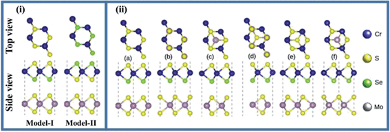 | ||
| Fig. 1 Side view and top view of (i) two models (ii) possible stacking patterns (a–f) of MS2–CrSSe (see text for details). | ||
To further confirm the energetic stability of the most feasible configuration, the binding energy is calculated for each configuration of both models of MS2–CrSSe vdW heterostructures. The binding energy is defined as:
| Eb = Ehetero − ETMDC − ECrSSe |
| Heterostructure | Model-I | Model-II | ||
|---|---|---|---|---|
| MoS2–CrSSe | WS2–CrSSe | MoS2–CrSeS | WS2–CrSeS | |
| a (Å) | 3.145 | 3.14 | 3.145 | 3.14 |
| d Mo–S/W–S (Å) | 2.40196 | 2.40815 | 2.40194 | 2.40816 |
| d Cr–Se (Å) | 2.42303 | 2.42575 | 2.42312 | 2.42499 |
| d Cr–S (Å) | 2.30146 | 2.30436 | 2.30 | 2.30375 |
| E (b) (eV) | −0.200 | −0.253 | −0.180 | −0.283 |
| h spacing (Å) | 3.2 | 3.0 | 3.1 | 3.0 |
| E g-PBE (eV) | 0.60 | 0.31 | 0.32 | 0.65 |
| E g-HSE (eV) | 1.60 | 1.07 | 1.14 | 1.48 |
| Φ (eV) | 3.79 | 3.39 | 3.59 | 3.79 |
| ΔV (eV) | 0.46 | 0.07 | 0.14 | 0.57 |
| E CBM (eV) | −0.23 | 0.13 | 0.01 | −0.08 |
| E VBM (eV) | 1.38 | 1.20 | 1.14 | 1.41 |
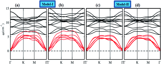
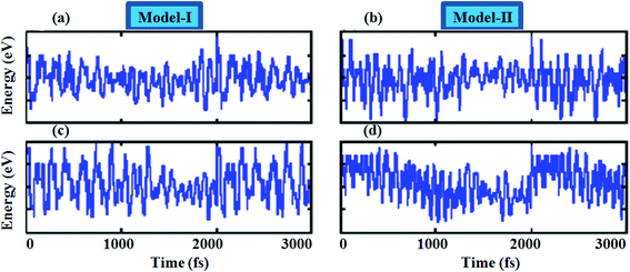
To assess the dynamical stability of MS2–CrSSe heterobilayers, the phonon band spectra is calculated using the phonopy code, as shown in Fig. 2. There are six atoms per primitive unit cell therefore, each phonon band dispersion is composed of three acoustic zero frequency modes and 15 optical branches. As it is clear from Fig. 2 that all phonon modes with positive eigenfrequencies at the Γ-point of the Brillouin zone indicates dynamical stability of MS2–CrSSe heterobilayers. This confirms the synthesis of all MS2–CrSSe heterobilayers. Further, the thermal stability of a material is important to study the molecular vibrations or fluctuation in energy with time at different temperatures.52,53 The thermal stability of MS2–CrSSe systems, presented in Fig. 3(a–d), is carried out by performing ab initio molecular dynamics (AIMD) calculations. Since it determines the amount of energy per vibrational degree of freedom and the oscillation amplitudes are dependent on the temperature. Both models of MS2–CrSSe systems comprise pure harmonic oscillators, revealing no prominent change in the energy spectra, as shown in Fig. 3(a–d). This indicates the absence of broken bonds or the reconstruction of geometric structures after heating the system at 300 K for 3000 fs, hence confirming the thermodynamical stability of the MS2–CrSSe systems. This behavior has also been demonstrated in P–SiS, P–SiC and P-Janus structures.54
In general, the electronic properties of 2D materials can be modulated by the interaction between the stacked monolayers. The electronic band structure of MS2–CrSSe systems is investigated using PBE and HSE06 functionals, as displayed in Fig. 4(a–d). All understudy systems possess an indirect band gap semiconducting nature with the valence band maximum (VBM) located at K-point and the conduction band maximum (CBM) found at Γ-point of the Brillouin zone. In this case, the excited electrons could jump from the valence band to the conduction band at K-point and then the holes move from Γ-point, which can effectively retard the combination of photogenerated electrons and holes and enhance the photocatalytic performance55 TMDCs.56,57 This is consistent with other 2D In2X3 (X = S, Se, Te) monolayers58 and Nb2XTe4.59 The band gap values of MS2–CrSSe (model-I and model-II) systems using PBE and HSE06 functionals are listed in Table 1. Evidently, an enlarged band gap value using the HSE06 level can be seen. This trend has been demonstrated in GeC–MS2 and SiC–MX2 systems.24,60,61 Further, the MS2–CrSSe vdW heterostructures with indirect type-I band gaps are comparatively more promising for photodetectors and photocatalysis as compared to MX2–Zr2CO2,62 PbI2–α-Te63 and GaS–g-C3N4 (ref. 64) vdWs heterostructures.
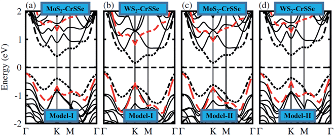 | ||
| Fig. 4 (a–d) Electronic band structures of MS2–CrSSe heterostructures and the black (red) dashed lines represent the PBE (HSE06) functional. | ||
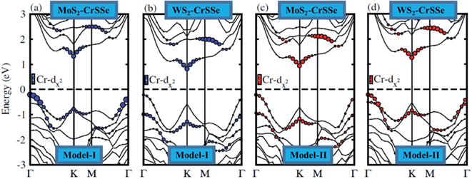
In order to illuminate the orbital character for understanding the nature of the band alignment of heterostructures, the weighted band structure of all heterobilayers is calculated, as displayed in Fig. 5. For both models of MS2–CrSSe systems, VBM and CBM are mainly attributed by the Cr-dz2 state. It is evident from Fig. 5(a–d) that both VBM and CBM are localized in the CrSSe monolayer of the studied systems, indicating the type-I band alignment in MS2–CrSSe heterobilayers. The formation of the type-I band alignment is crucial for lasers or light emitting diodes (LEDs) applications.65 A similar trend of type-I band alignment has been theoretically demonstrated in ZnO–JTMDC, phosphorene–ZrSSe, and WSSe–WX2 (ref. 66–68) and experimentally reported in MoS2–PbI2.69
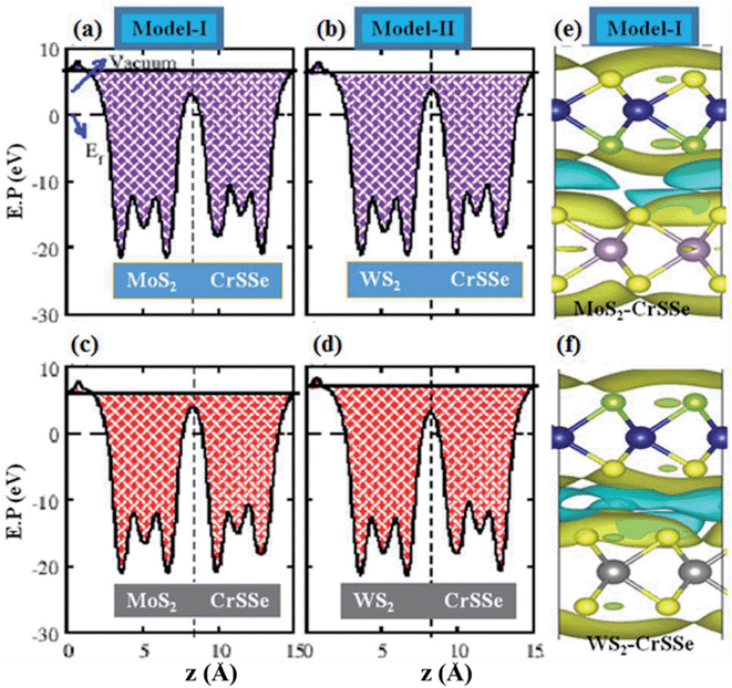
The absence of mirror-symmetry in Janus 2D materials results in different polarization effects, which helps to understand the intrinsic electronic and extrinsic photocatalytic behavior of the materials.70–73 The plane-averaged electrostatic potential of all MS2–CrSSe heterobilayers for both models is calculated and plotted in Fig. 6(a–d). It can be clearly seen that all MS2–CrSSe heterobilayers have different potential energies with different positions of S- and Se-atoms in CrSSe in both models and results in different work functions (Φ) at S and Se atoms in CrSSe, as listed in Table 1. The calculated work function of understudy heterobilayers is comparatively smaller than the work functions of corresponding parent monolayers (5.15 eV (MoS2), 4.09 eV (WS2) and 5.24 eV (CrSSe) reported in ref. 23 and 38) and leads to strong interfacial interaction. In models-I, electrons may transfer from MoS2(WS2) with deeper potential to CrSSe with a lower potential, forming a built-in electric field at the interface with a potential drop of 0.46 eV(0.07 eV). Similarly, the potential drop (ΔV) for MoS2(WS2)–CrSeS is 0.14 eV(0.57 eV), which is consistent with C4N–MoS2.74 The built-in electric field formed at the interface moves from the MS2 (M = Mo, W) layer to the CrSSe layer for both model-I and model-II. Further, the charge density difference (Δρ = ρMS2–CrSSe − ρMS2 − ρCrSSe) of the MS2–CrSSe system is calculated to address the interlayer charge transfer, as plotted in Fig. 6(e and f). Here, ρMS2–CrSSe, ρMS2 and ρCrSSe represent the charge density of MS2–CrSSe, MS2 and CrSSe systems, respectively. In Fig. 6(e and f), the gain and loss of electrons are represented by yellow and cyan colors, respectively. It can be easily seen that MS2 depletes charges and the CrSSe layer accumulates charges. However, the main charge redistribution occurs in the interfacial region between chalcogen atoms of the individual layers, indicating a built-in electric field in the interfacial region. In both models, MS2–CrSSe heterobilayers exhibit the same character of charge transfer; hence, Δρ is plotted only for model-I of the Mo(W)S2–CrSSe system (Fig. 6(e and f)). This identifies that P-type doping occurs in MS2 monolayers. Moreover, the Bader charge analysis reveals that an amount of 0.0005e (0.0025e) is driven from MoS2 to CrSSe in model-I (model-II) and 0.0089e (0.0021e) is donated by WS2 to CrSSe in model-I (model-II). Interestingly, charge transfer in model-I (model-II) is responsible for stronger electronic influence in the WS2 (MoS2) monolayer.
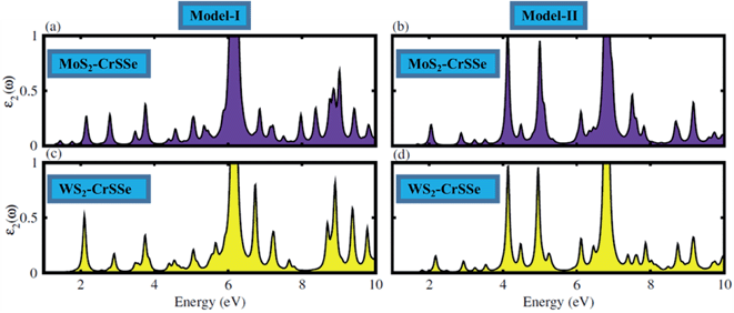
The optical response of materials to incident solar light is crucial in identifying the promising materials for the water splitting mechanism. The optical parameter particularly the imaginary part of the dielectric function ε2(ω) of understudy systems is calculated to understand the transition between the occupied and unoccupied states, as displayed in Fig. 7(a–d). The electronic band structure is modified in the MS2–CrSSe system due to the weak coupling and interlayer charge transfer between the pristine monolayers. Moreover, the excitons dominate the optical transition from the valence band (VB) to the conduction band (CB) in all understudy heterostructures. Interestingly, the excitonic transition occurs in the range of 1.07–1.60 eV for MoS2–CrSSe, 2.05–2.80 eV for WS2–CrSSe, 2.01–2.80 eV for MoS2–CrSeS and 3.0–3.5 eV for WS2–CrSeS. In contrast to pristine monolayers, a red-shift is evidently observed in the optical absorption spectra of MS2–CrSSe, highlighting them as potential candidates for optoelectronic devices to capture the visible solar spectrum. Other 2D materials have followed the same trend.75–78
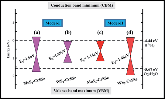
To explore water dissociation into hydrogen production under solar irradiation, the valence band (VB) edge and conduction band (CB) edge position align with the standard reduction (H+/H2) and oxidation (O2/H2O) potentials of water dissociation are calculated at pH = 0 using the HSE06 level, as displayed in Fig. 8. In general, the standard potentials for the redox reactions of water splitting are as follows Ered (H+/H2) = −4.44 eV + pH × 0.059 eV and EOx (O2/H2O) = −5.67 eV + pH × 0.059 eV.79 In photocatalysis, photogenerated electrons and holes are separated and transported to H+/H2 or to O2 molecules. For the water splitting reaction, the photocatalyst should possess a semiconducting band gap with a value greater than 1.23 eV. Evidently, for W(Mo)S2–CrSSe of model-I(II), the valence band (VB) edge is found above the oxidation potential and the conduction band (CB) edge fails to reside above the reduction potential. In contrast, for other Mo(W)S2–CrSSe systems of model-I(II), the CBM lies higher than the reduction potential (−4.50 eV) and the VBM is located lower than the oxidation potential (−5.70 eV). This exciting trend of the band edge position has been demonstrated for other materials.80,81 Hence, both VB and CB edges straddle the redox potentials, rendering these systems as suitable candidates for producing low cost hydrogen gas at a commercial scale.
Conclusion
To summarize, we theoretically investigated the structural, electronic, optical and photocatalytic behavior of two different models of MS2–CrSSe (M = Mo, W) heterostructures by performing the density functional theory calculations. The feasible binding energy, absence of imaginary frequencies in phonon branches and no considerable fluctuation of the energy curve at room temperature verify the energetic and dynamical stability of all understudy heterobilayers. All MS2–CrSSe (M = Mo, W) systems possess an indirect type-I band alignment with VBM and CBM localized in the CrSSe layer, indicating the recombination of photogenerated electrons and holes in the CrSSe layer, hence making them suitable for light detection applications. The broadening of light absorption in the visible region coupled with red-shift in absorption spectra reveals MS2–CrSSe systems promising for light conversion purposes. The Mo(W)S2–CrSSe of model-I(II) heterobilayers are capable of performing redox reactions of water splitting under solar irradiation, whereas the WS2(MoS2)–CrSSe system of model-I(II) fails to perform redox reactions. These findings lead to the practical utilization of MS2–CrSSe systems in future optoelectronic and photocatalytic water splitting applications.Conflicts of interest
The authors declare no conflict of interest.References
- G. A. Konstantin, Science, 2009, 324(5934), 1530–1534 CrossRef PubMed.
- R. Mas-Balleste, C. Gomez-Navarro, J. Gomez-Herrero and F. Zamora, Nanoscale, 2011, 3(1), 20–30 RSC.
- S. Dervin, D. D. Dionysiou and S. C. Pillai, Nanoscale, 2016, 8(33), 15115–15131 RSC.
- C. Jin, F. Lin, K. Suenaga and S. Iijima, Phys. Rev. Lett., 2009, 102(19), 195505 CrossRef PubMed.
- Y. Khan, S. M. Obaidulla, M. R. Habib, A. Gayen, T. Liang, X. Wang and M. Xu, Nano Today, 2020, 34, 100902 CrossRef CAS.
- J. D. Yao and G. W. Yang, Nano Today, 2021, 36, 101026 CrossRef CAS.
- M. Mattinen, M. Leskelä and M. Ritala, Adv. Mater. Interfaces, 2021, 8(6), 2001677 CrossRef CAS.
- P. V. Shinde, A. Kumar, D. J. Late and C. S. Rout, J. Mater. Chem. C, 2021, 9(11), 3773–3794 RSC.
- S. G. Seo, J. Jeong, S. Y. Kim, A. Kumar and S. H. Jin, Nano Res., 2021, 14(9), 3214–3227 CrossRef CAS.
- N. N. Rosman, R. M. Yunus, L. J. Minggu, K. Arifin, M. N. I. Salehmin, M. A. Mohamed and M. B. Kassim, Int. J. Hydrogen Energy, 2018, 43(41), 18925–18945 CrossRef CAS.
- W. Lei, S. Zhang, G. Heymann, X. Tang, J. Wen, X. Zheng, G. Hu and X. Ming, J. Mater. Chem. C, 2019, 7(7), 2096–2105 RSC.
- X. Wan, E. Z. Chen, J. Yao, M. Gao, X. Miao, S. Wang and Y. Gu, et al. , ACS Nano, 2021, 15(12), 20319–20331 CrossRef CAS PubMed.
- Z. Cai, B. Liu, X. Zou and H.-M. Cheng, Chem. Rev., 2018, 118(13), 6091–6133 CrossRef CAS PubMed.
- R. Li, Y. Cheng and W. Huang, Small, 2018, 14, 1802091 CrossRef PubMed.
- S. Ahmad, I. Shahid, N. Shehzad, W. Khan, H. U. Din, M. Idrees, B. Amin and A. Laref, RSC Adv., 2022, 12, 11202–11206 RSC.
- M. Idrees, H. U. Din, R. Ali, G. Rehman, T. Hussain, C. V. Nguyen and B. Amin, Phys. Chem. Chem. Phys., 2019, 21, 18612–18621 RSC.
- B. Javvaji, B. He, X. Zhuang and H. S. Park, Phys. Rev. Mater., 2019, 3, 125402 CrossRef CAS.
- L. Ju, M. Bie, J. Shang, X. Tang and L. Kou, J. Phys.: Mater., 2020, 3, 022004 CAS.
- S. B. Yu, M. Zhou, D. Zhang and K. Chang, Phys. Rev. B, 2021, 104, 075435 CrossRef CAS.
- W. Z. Xiao, L. Xu, G. Xiao, L. L. Wang and X. Y. Dai, Phys. Chem. Chem. Phys., 2020, 22, 14503–14513 RSC.
- H. W. Guo, Z. Hu, Z. B. Liu and J. G. Tian, Adv. Funct. Mater., 2021, 31, 2007810 CrossRef CAS.
- Y. Guo, L. Wu, J. Deng, L. Zhou, W. Jiang, S. Lu and C. Zhang, Nano Res., 2022, 15, 1276–1281 CrossRef CAS.
- Q. Zhuang, J. Li, C. He, T. Ouyang, C. Zhang, C. Tang and J. Zhong, Nanoscale Adv., 2021, 3, 3643–3649 RSC.
- H. U. Din, M. Idrees, A. Albar, M. Shafiq, I. Ahmad, C. V. Nguyen and B. Amin, Phys. Rev. B, 2019, 100, 165425 CrossRef CAS.
- W. Xia, L. Dai, P. Yu, X. Tong, W. Song, G. Zhang and Z. Wang, Nanoscale, 2017, 9, 4324–4365 RSC.
- W. Wei, Y. Dai, Q. Sun, N. Yin, S. Han, B. Huang and T. Jacob, Phys. Chem. Chem. Phys., 2015, 17, 29380–29386 RSC.
- W. Wei, Y. Dai and B. Huang, Phys. Chem. Chem. Phys., 2017, 19, 663–672 RSC.
- K. Ren, S. Wang, Y. Luo, J. P. Chou, J. Yu, W. Tang and M. Sun, J. Phys. D: Appl. Phys., 2020, 53, 185504 CrossRef CAS.
- M. Torrent, N. A. W. Holzwarth, F. Jollet, D. Harris, N. Lepley and X. Xu, Comput. Phys. Commun., 2010, 181, 1862–1867 CrossRef CAS.
- B. Liu, X. Wang, J. L. Xu, D. Tian, R. Y. Chen, J. Xu and X. H. Buab, Phys. Rev. B: Condens. Matter Mater. Phys., 1994, 49, 16223–16233 CrossRef PubMed.
- G. Kresse and J. Furthmüller, Phys. Rev. B: Condens. Matter Mater. Phys., 1996, 54, 11169 CrossRef CAS PubMed.
- J. P. Perdew, K. Burke and M. Ernzerhof, Phys. Rev. Lett., 1996, 77, 3865 CrossRef CAS PubMed.
- J. Heyd, G. E. Scuseria and M. Ernzerhof, J. Chem. Phys., 2003, 118, 8207–8215 CrossRef CAS.
- J. Antony and S. Grimme, Phys. Chem. Chem. Phys., 2006, 8, 5287–5293 RSC.
- H. J. Monkhorst and J. D. Pack, Phys. Rev. B: Solid State, 1976, 13, 5188 CrossRef.
- A. Togo, F. Oba and I. Tanaka, Phys. Rev. B: Condens. Matter Mater. Phys., 2008, 78, 134106 CrossRef.
- G. Henkelman, A. Arnaldsson and H. Jónsson, Comput. Mater. Sci., 2006, 36, 354–360 CrossRef.
- S. Grimme, J. Comput. Chem., 2006, 27, 1787 CrossRef CAS PubMed.
- X.-H. Li, B.-J. Wang, X.-L. Cai, W.-Y. Yu, L.-W. Zhang, G.-D. Wanga and S.-H. Ke, RSC Adv., 2017, 7, 44394–44400 RSC.
- C. V. Nguyen and N. N. Hieu, Chem. Phys., 2016, 468, 9–14 CrossRef CAS.
- B. Amin, T. P. Kaloni and U. Schwingenschlögl, RSC Adv., 2014, 4, 34561–34565 RSC.
- H. U. Din, M. Idrees, Q. Alam and B. Amin, Appl. Surf. Sci., 2021, 568, 150846 CrossRef CAS.
- K. F. Mak, C. Lee, J. Hone, J. Shan and T. F Heinz, Phys. Rev. Lett., 2010, 105, 136805 CrossRef PubMed.
- A. Splendiani, L. Sun, Y. Zhang, T. Li, J. Kim, C. Y. Chim, G. Galli and F. Wang, Nano Lett., 2010, 10, 1271–1275 CrossRef CAS PubMed.
- M. R. Molas, K. Nogajewski, A. O. Slobodeniuk, J. Binder, M. Bartos and M. Potemski, Nanoscale, 2017, 9, 13128–13141 RSC.
- W. Zhao, et al., Evolution of electronic structure in atomically thin sheets of WS2 and WSe2, ACS Nano, 2013, 7, 791–797 CrossRef CAS PubMed.
- Q. H. Wang, K. Kalantar-Zadeh, A. Kis, J. N. Coleman and M. S. Strano, Nat. Nanotechnol., 2012, 7, 699 CrossRef CAS PubMed.
- X. Hong, J. Kim, S. F. Shi, Y. Zhang, C. Jin, Y. Sun, S. Tongay, J. Wu, Y. Zhang and F. Wang, Nat. Nanotechnol., 2014, 9, 682–686 CrossRef CAS PubMed.
- P. Tonndorf, R. Schmidt, P. Böttger, X. Zhang, J. Börner, A. Liebig, M. Albrecht, C. Kloc, O. Gordan, D. R. T. Zahn, S. M. de Vasconcellos and R. Bratschitsch, Opt. Express, 2013, 21, 4908–4916 CrossRef CAS PubMed.
- Q. Luan, C.-L. Yang, M.-S. Wang and X.-G. Ma, Chin. J. Phys., 2017, 55(5), 1930–1937 CrossRef CAS.
- H. R. Gutierrez, N. P. P. Lopez, A. L. Elías, A. Berkdemir, B. Wang, R. Lv, F. López-Urías, V. H. Crespi, H. Terrones and M. Terrones, Nano Lett., 2013, 13(8), 3447–3454 CrossRef CAS PubMed.
- I. Ahmad, S. A. Khan, M. Idrees, M. Haneef, I. Shahid, H. U. Din and B. Amin, Phys. B, 2018, 545, 113–118 CrossRef CAS.
- B. Fallahazad, H. C. Movva, K. Kim, S. Larentis, T. Taniguchi, K. Watanabe and E. Tutuc, Phys. Rev. Lett., 2016, 116, 086601 CrossRef PubMed.
- A. Devi, A. Kumar, A. Singh and P. K. Ahluwalia, AIP Conf. Proc., 2020, 1, 030701 CrossRef.
- H.-L. Liu, T. Yang, J.-H. Chen, H.-W. Chen, H. Guo, R. Saito, M.-Y. Li and L.-J. Li, Sci. Rep., 2020, 10(1), 1–11 CrossRef PubMed.
- G. Wang, A. Chernikov, M. M. Glazov, T. F. Heinz, X. Marie, T. Amand and B. Urbaszek, Rev. Mod. Phys., 2018, 90, 021001 CrossRef CAS.
- D. Erben, A. Steinhoff, C. Gies, G. Schönhoff, T. O. Wehling and F. Jahnke, Phys. Rev. B, 2018, 98, 245203 CrossRef.
- W.-Y. Fang, P. An Li, J.-H. Yuan, K.-H. Xue and J.-F. Wang, J. Electron. Mater., 2020, 49(2), 959–968 CrossRef CAS.
- P. Zhao, Y. Ma, X. Lv, M. Li, B. Huang and Y. Dai, Nano Energy, 2018, 51, 533–538 CrossRef CAS.
- H. U. Din, M. Idrees, G. Rehman, C. V. Nguyen, L. Y. Gan, I. Ahmad and B. Amin, Phys. Chem. Chem. Phys., 2018, 20, 24168–24175 RSC.
- M. Idrees, M. Fawad, M. Bilal, Y. Saeed, C. V. Nguyen and B. Amin, RSC Adv., 2020, 10, 25801–25807 RSC.
- G. Rehman, S. A. Khan, B. Amin, I. Ahmad, Li.-Y. Gan and M. Maqbool, J. Mater. Chem. C, 2018, 6, 2830–2839 RSC.
- M. M. Obeid, Appl. Surf. Sci., 2020, 508, 144824 CrossRef CAS.
- K. Bai, Z. Cui, E. Li, Y. Ding, J. Zheng, C. Liu and Y. Zheng, Vacuum, 2020, 180, 109562 CrossRef CAS.
- S. Lee, J.-E. Jung, H.-G. Kim, Y. Lee, J. M. Park, J. Jang, S. Yoon, A. Ghosh, M. Kim, J. Kim, W. Na, J. Kim, H. J. Choi, H. Cheong and K. Kim, Nano Lett., 2021, 21(10), 4305–4313 CrossRef CAS PubMed.
- M. Idrees, H. U. Din, S. U. Rehman, M. Shafiq, Y. Saeed, H. D. Bui and B. Amin, Phys. Chem. Chem. Phys., 2020, 22, 10351–10359 RSC.
- T. A. Alrebdi and B. Amin, Chem. Phys., 2021, 549, 111252 CrossRef CAS.
- M. Hetterich, M. D. Dawson, A. Y. Egorov, D. Bernklau and D. H. Riechert, Appl. Phys. Lett., 2000, 76, 1030–1032 CrossRef CAS.
- S. Ding, X. Xiao, S. Liu, J. Wu, Z. Huang, X. Qi and J. Li, Appl. Phys. A: Mater. Sci. Process., 2019, 125, 1–7 CrossRef.
- Q. F. Yao, J. Cai, W. Y. Tong, S. J. Gong, J. Q. Wang, X. Wan and X. J. H. Chu, Phys. Rev. B, 2017, 95, 165401 CrossRef.
- A. Kandemir and A. H. Sahin, Phys. Rev. B, 2018, 97, 155410 CrossRef CAS.
- F. Ersan and C. Ataca, Phys. Rev. Appli., 2020, 13, 064008 CrossRef CAS.
- W. Ju, D. Wang, T. Li, Y. Zhang, Z. Gao, L. Ren and S. Gong, Phys. Chem. Chem. Phys., 2020, 22, 9148–9156 RSC.
- M. Yang, L. Wang, T. Hou and Y. Li, J. Mater. Chem. C, 2017, 5, 201–207 RSC.
- X. Zhang, Y. Song, F. Zhang, Q. Fan, H. Jin, S. Chen and W. Zhang, Mater. Res. Express, 2019, 6, 105055 CrossRef CAS.
- A. L. Elías, N. Perea-López, A. Castro-Beltrán, A. Berkdemir, R. Lv, S. Feng and M. Terrones, ACS Nano, 2013, 7, 5235–5242 CrossRef PubMed.
- A. Ramasubramaniam, Phys. Rev. B: Condens. Matter Mater. Phys., 2012, 86, 115409 CrossRef.
- H. Shi, H. Pan, Y. W. Zhang and B. I. Yakobson, Phys. Rev. B: Condens. Matter Mater. Phys., 2013, 87, 155304 CrossRef.
- A. Molina-Sánchez, D. Sangalli, K. Hummer, A. Marini and L. Wirtz, Phys. Rev. B: Condens. Matter Mater. Phys., 2013, 88, 045412 CrossRef.
- M. M. Asmar and S. E. Ulloa, Phys. Rev. B: Condens. Matter Mater. Phys., 2014, 112(13), 136602 Search PubMed.
- F. Zheng, L. Z. Tan, S. Liu and A. M. Rappe, Nano Lett., 2015, 15, 7794–7800 CrossRef CAS PubMed.
| This journal is © The Royal Society of Chemistry 2022 |

