
 Open Access Article
 This Open Access Article is licensed under a Creative Commons Attribution-Non Commercial 3.0 Unported Licence
Te/SnS2 tunneling heterojunctions as high-performance photodetectors with superior self-powered properties†
Xuanhao
Cao
a,
Zehong
Lei
a,
Shuting
Zhao
a,
Lili
Tao
a,
Zhaoqiang
Zheng
 a,
Xing
Feng
a,
Jingbo
Li
b and
Yu
Zhao
*a
a,
Xing
Feng
a,
Jingbo
Li
b and
Yu
Zhao
*a
aGuangdong Provincial Key Laboratory of Information Photonics Technology, Guangdong Provincial Key Laboratory of Functional Soft Condensed Matter, School of Material and Energy, Guangdong University of Technology, Guangzhou 510006, China. E-mail: zhaoyu@gdut.edu.cn
bGuangdong Key Lab of Chip and Integration Technology, Institute of Semiconductors, South China Normal University, Guangzhou 510631, P. R. China
First published on 29th August 2022
Abstract
The tunneling heterojunctions made of two-dimensional (2D) materials have been explored to have many intriguing properties, such as ultrahigh rectification and on/off ratio, superior photoresponsivity, and improved photoresponse speed, showing great potential in achieving multifunctional and high-performance electronic and optoelectronic devices. Here, we report a systematic study of the tunneling heterojunctions consisting of 2D tellurium (Te) and Tin disulfide (SnS2). The Te/SnS2 heterojunctions possess type-II band alignment and can transfer to type-III one under reverse bias, showing a reverse rectification ratio of about 5000 and a current on/off ratio over 104. The tunneling heterojunctions as photodetectors exhibit an ultrahigh photoresponsivity of 50.5 A W−1 in the visible range, along with a dramatically enhanced photoresponse speed. Furthermore, due to the reasonable type-II band alignment and negligible band bending at the interface, Te/SnS2 heterojunctions at zero bias exhibit excellent self-powered performance with a high responsivity of 2.21 A W−1 and external quantum efficiency of 678%. The proposed heterostructure in this work provides a useful guideline for the rational design of a high-performance self-powered photodetector.
Introduction
Two-dimensional (2D) materials, such as graphene, transition metal dichalcogenides (TMDs), and black phosphorus (BP), have attracted extensive attention due to their outstanding properties and wide range of applications in electronic and optoelectronic devices.1,2 van der Waals heterojunctions (vdWHs) formed by stacking of layered 2D materials not only offer new properties, such as tunable band structure,3,4 charge transfer5,6 and new optical absorption,7 but also preserve the unique properties of their building blocks, giving them great potential for applications in many diverse fields, including electronics,8,9 optoelectronics,10–13 catalysis,14,15 and energy harvesting.16 The built-in electric field at the interface of a heterojunction provides a driving force to efficiently separate the photogenerated electron–hole pairs, making vdWH a potential high-performance photodetector through proper band alignment design. VdWHs constructed using most of the 2D TMDs tend to form a type-II band alignment, which is beneficial for the modulation of interlayer energy transition and the separation of spatial charge. Typically, MoS2/WS2 (ref. 17) and MoS2/BP18 vdWHs exhibit strong interlayer coupling and have comparable photoresponsivity of 2.3 and 22.3 A W−1 in the visible range, respectively. On the other hand, type-III (broken gap) heterojunctions, which can induce band-to-band tunneling of the photoinduced carrier at the interface, have drawn special attention due to their unique properties of ultrahigh reverse rectification and ultralow forward current.13,19–23 In order to construct a tunneling structure, a narrow-band gap semiconductor material (e.g., AsP, BP, PtS2,etc.) is chosen as one of the channel materials. However, the large dark current and ultrafast electron–hole recombination rate originating from the narrow-bandgap nature hinder the enhancement of photoresponsivity in tunneling vdWHs. Hence, in spite of excellent rectification properties, most of the reported tunneling vdWHs, including Bi2Se3/MoTe2,19 PtS2/WSe2,20 AsP/InSe,21 and BP/ReS2,22 show moderate photoresponsivity ranging from 8 mA W−1 to 2.49 A W−1. In our previous work, we intentionally constructed a non-layered Te/SnS2 tunneling heterojunction to utilize the photogating effect, with which we successfully achieved an ultrahigh photoresponsivity of 146 A W−1 along with enhanced response speed.4 Furthermore, self-powered photodetectors can detect light without an external power supply, which has important applications in scenarios that have limited energy source.24 The heterostructure-based self-powered photodetector, which can work well by the irradiation of light from ultraviolet (UV)25–28 to infrared,29 has been widely studied. However, due to the same above-mentioned reasons, the reported tunneling vdWHs exhibited zero-bias photoresponsivity below 1 A W−1, which is too small for practical self-powered applications. It is still a challenge to obtain tunneling-heterojunction-based high-performance photodetectors with excellent self-powered properties.2D tellurium (Te) is a p-type material with a thickness-dependent bandgap (0.35–1.04 eV).31 It has many intriguing properties, such as excellent photoresponse to infrared irradiation,29,30 ambipolar electrical transport behavior,31 high field-effect hole mobility exceeds 800 cm2 V−1 s−1,32 and superior air stability enabled by the inherent chiral-chain structure along the c-axis. On the other hand, tin disulfide (SnS2) is an intrinsic n-type semiconductor material with an indirect bandgap of 2.07 eV.33 It exhibits high electron mobility up to 230 cm2 V−1 s−1 (ref. 34) and a high optical absorption coefficient exceeding 104 cm−1 in the visible region,35 making it a promising channel material for the photodetector. More importantly, when combining these two materials to form a heterostructure, the valence-band maximum (Ev) of the SnS2 is very close to the conduction band minimum (Ec) of the Te, which is beneficial for the efficient separation of the photo-induced electron–hole pairs.
Here, we report a tunneling heterojunction consisting of 2D Te and SnS2 flakes, which can function as a high-performance backward diode and photodetector. The Te/SnS2 heterojunctions possess type-II band alignment and can transfer to type-III at reverse bias, showing typical reverse rectification characteristics. The heterojunctions used as a photodetector exhibit excellent optical response to visible light with a maximal responsivity of 50.5 A W−1 and detectivity of 1.15 × 10¹¹ jones under irradiation of 405 nm laser. Due to the reasonable band alignment of the type-II structure and negligible band bending at the interface, the Te/SnS2 tunneling heterojunctions demonstrate superior self-powered properties with a high responsivity of 2.21 A W−1 and external quantum efficiency of 678% at zero bias, which exceed the self-powered performance of all the reported photodetectors based on tunneling vdWHs.
Results and discussion
The Te flakes were grown on a mica substrate by the physical vapor deposition (PVD) method while SnS2 flakes were prepared by mechanical exfoliation followed by the polydimethylsiloxane (PDMS) assisted dry alignment transfer method. SnS2 and Te flakes were then sequentially transferred onto the 300 nm SiO2/Si substrate to form a vertical stacking via a wet transfer process. 50 nm layer of Au, as electrodes, was deposited in the photolithography-defined patterned area by thermal evaporation. The details of the materials preparation and device fabrication can be seen in the Experimental section. The conductance types of Te and SnS2 were testified (S1 and S2 in the ESI†), which proved to be p-type and n-type respectively. X-ray diffraction (XRD), X-ray photoelectron spectroscopy (XPS), and high-resolution transmission electron microscopy (HRTEM) were used to characterize the constituent materials Te and SnS2, results of which are shown in Fig. 1. As seen in the XRD pattern shown in Fig. 1(a), the very sharp four peaks located at 23.1°, 27.6°, 40.4°, and 47.1° correspond to (100), (101), (110) and (200) planes of Te (ICSD 97-008-0004), respectively, suggesting the high quality of the PVD-grown Te. The binding energies for Te 3d5/2 and Te 3d3/2 shown in Fig. 1(b) are located at 573.2 eV and 583.5 eV, respectively, with ΔE of 10.3 eV, agreeing well with the previously reported results on Te.36 The lattice spacing of 0.38 nm seen in the HRTEM image in Fig. 1(c) is in accordance with the (100) interplanar distance of Te. In addition, the in situ selected area electron diffraction (SAED) in the inset of Fig. 1(c) shows a set of regular hexagonal patterns, suggesting again the single-crystalline nature of Te. Similarly, Fig. 1(d) shows four main XRD peaks located at 15.1°, 30.4°, 46.2°, and 63.1°, corresponding to (100), (002), (003) and (004) planes, respectively, of SnS2 (ICSD 97-004-3004). The peaks at 161.80 eV and 162.95 eV in the XPS image of Fig. 1(d) belong to S 2p3/2 and S 2p1/2, respectively, and those at 486.85 eV and 495.25 eV belong to Sn 3d5/2 and Sn 3d3/2, respectively. The HRTEM image of Fig. 1(f) shows a lattice spacing of 0.32 nm, corresponding to the (100) plane of the hexagonal structure SnS2.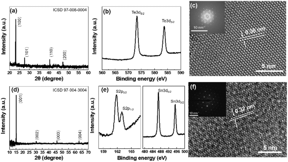 | ||
| Fig. 1 (a) XRD patterns, (b) XPS patterns, and (c) HRTEM image with the inset of SAED patterns of synthesized Te flakes. (d) XRD patterns, (e) XPS patterns, and (f) HRTEM image with the inset of SAED patterns of mechanically-exfoliated SnS2 flakes. | ||
Fig. 2(a) and (b) show the schematic diagram and optical microscopy image of the Te/SnS2 heterojunction, respectively. The Te flakes are specifically on top of the SnS2 for a more efficient separation of the photoinduced electron–hole pairs (discussed later). As shown in the inset of Fig. 2(b), the thickness of Te and SnS2 flakes, as revealed from the atomic force microscopy (AFM) measurements, was estimated to be 92 nm and 67 nm, respectively. Fig. 2(c) shows the Raman spectra measured on the surface of the Te side, SnS2 side, and overlap area in a single heterostructure. Te flakes have three vibration peaks located at 89.2 cm−1, 118.6 cm−1, and 137.2 cm−1, corresponding to E1, A1 and E2 vibration modes, respectively. SnS2 flakes have one characteristic peak at 312.3 cm−1. Those Raman peaks are in accordance with the previous reports of Te32,37 and 2H–SnS2.38 The Raman spectrum of the heterojunction exhibits a combination of the phonon vibration modes of its two constituent materials with slightly reduced intensity and negligible peak shift.
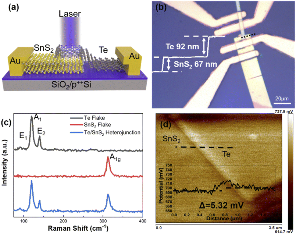 | ||
| Fig. 2 (a) The schematic diagram of the Te/SnS2 heterostructure as a photodetector. (b) The optical microscope image of the Te/SnS2 heterostructure with an effective channel area of 76 μm2 and an inset of the thickness height profile measured by AFM. (c) The Raman spectra of the Te/SnS2 heterostructure on the Te side, SnS2 side, and overlap area, respectively. (d) The potential difference between Te and SnS2 with an inset of the potential height profile. | ||
A Kelvin probe force microscope (KPFM) was used to measure the built-in contact potential difference at the interface between Te flakes and SnS2 flakes, as shown in Fig. 2(d). The surface potential distribution (SPD) of Te and SnS2 flakes with respect to the tip of AFM can be expressed in the form of the following equations:
| eSPDSnS2 = Wtip − WSnS2 | (1) |
| eSPDTe = Wtip − WTe | (2) |
| ΔEf = WTe − WSnS2 = eSPDSnS2 − eSPDTe | (3) |
The work function difference between Te and SnS2 (see the inset of Fig. 2(d)) is as small as 5.32 meV. As the work function of the AFM tip is about 3.65 eV, the work functions of Te and SnS2 can be calculated to be about 4.350 eV and 4.345 eV, respectively. On the other hand, the valence-band maximum (denoted by Ev) of Te and SnS2 with respect to the vacuum level are −4.38 eV and −6.28 eV, respectively, obtained by linearly extrapolating the low-binding energy region of the XPS spectra to the baseline (Fig. S3†). The reported indirect bandgap energy of SnS2 is 2.07 eV,33 while the bandgap energy of bulk Te is about 0.36 eV.39 Hence, with the above band information, the relative band positions of SnS2 and Te, before and after the contact can be drawn and illustrated in Fig. 3(c) and (d). The stacking of Te/SnS2 was found to be a PN junction with the band arrangement of the type-II heterostructure. It was noticed that the band structure had negligible band bending at the interface due to a very small energy difference (5.32 meV) between the Fermi levels of SnS2 and Te.
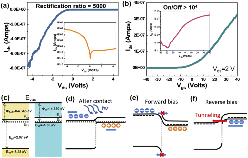 | ||
| Fig. 3 (a) The output (Ids–Vds) curve of the Te/SnS2 heterojunction at Vgs = 0 V with the same curve in the logarithmic plot as an inset. (b) The transfer (Ids–Vgs) curve of the Te/SnS2 heterojunction at Vds = 2 V with the same curve in the logarithmic plot as an inset. The energy band diagrams of SnS2 and Te (c) before and (d) after contact. Diagrams of the band alignment of Te/SnS2 heterojunction under (e) forward and (f) reverse bias. | ||
The electrical characteristics of the heterojunction devices including output and transfer curves were measured. As illustrated in Fig. 2(a), the electrode on the p-type Te is defined as the drain, while the other on n-type SnS2 is defined as the source. The 300 nm SiO2 on Si was used as a back gate. The output curve at Vgs = 0 in Fig. 3(a) shows a prominent reverse rectification characteristic with a rectification ratio of about 5000 at Vds = ±4 V. This unique behaviour of reverse rectification is a typical characteristic of a tunneling heterostructure.4,20,21,40,41 In addition, the transfer curve of the device in Fig. 3(b) shows a current on/off ratio over 104. Also, it exhibits an n-type-dominated characteristic with very weak bipolar behaviour, indicating that the conducting property of the device is mainly determined by the SnS2 channel. The working mechanism of the Te/SnS2 tunneling heterostructure is described as follows. As shown in Fig. 3(e), when under forward bias, the transport of electrons from SnS2 to Te is greatly blocked by the severe band bending at the interface and the large Schottky barrier built at the metal–SnS2 interface because of the Fermi level pinning effect. Hence, forward current is largely suppressed. When under the reverse bias, the downward pulling of the n-side band diagram results in a type-III band alignment (Fig. 3(f)), where electrons are allowed to transport from Te to SnS2 through band-to-band tunneling (BTBT) with the help of the external field. In this way, a large reverse current is produced in the device. To further confirm this tunneling mechanism, a theoretical I–V relation for the BTBT tunneling model21,42 is used to fit the experimental results in Fig. 3(a). As shown in Fig. S4,† the reverse current is well fitted by the relation  , confirming the tunneling mechanism of the electron transport under reverse bias.
The optical response of the Te/SnS2 tunneling heterostructure was systematically investigated. The photocurrents of the device at Vds = 2 V in response to periodic irradiation of 405, 532, 635, and 808 nm lasers are shown in Fig. 4(a)–(d), respectively. The photocurrent demonstrates a stable response of the device to the irradiation of all four wavelengths under different light power intensities. Parameters including responsivity, detectivity, and external quantum efficiency are used to evaluate the performance of the device in response to light. The responsivity Rλ refers to the photocurrent of the device generated per unit power of the incident light per unit area. The expression is as follows.
 | (4) |
 | (5) |
 | (6) |
![[thin space (1/6-em)]](https://www.rsc.org/images/entities/char_2009.gif) 500%, respectively, under irradiation by the 405 nm laser with the power density of 0.24 W m−2. The photocurrent can be expressed using the power-law Iph ∝ Pα to quantify the influence of the optical power density on the optical response, where α is the power index. By fitting the experimental data, the expression follows the relationship Iph (A) = 2.2 × 10⁹P0.55, where P is in the unit of W m−2. Furthermore, as shown in Fig. S5,† the heterojunction shows a steady response (deviation less than 10%) and negligible degradation after 500 continuous cycles of irradiation. Also, the heterojunction device can maintain excellent optical response after being exposed to air for two weeks (see Fig. S6†), showing good environmental stability. Since many studies have revealed the optical response of the Te-based photodetector to infrared light, we also measured the response of our Te/SnS2 heterojunction to a longer wavelength. It is found that the device almost has no response at 915 and 1550 nm (Fig. S7†).
500%, respectively, under irradiation by the 405 nm laser with the power density of 0.24 W m−2. The photocurrent can be expressed using the power-law Iph ∝ Pα to quantify the influence of the optical power density on the optical response, where α is the power index. By fitting the experimental data, the expression follows the relationship Iph (A) = 2.2 × 10⁹P0.55, where P is in the unit of W m−2. Furthermore, as shown in Fig. S5,† the heterojunction shows a steady response (deviation less than 10%) and negligible degradation after 500 continuous cycles of irradiation. Also, the heterojunction device can maintain excellent optical response after being exposed to air for two weeks (see Fig. S6†), showing good environmental stability. Since many studies have revealed the optical response of the Te-based photodetector to infrared light, we also measured the response of our Te/SnS2 heterojunction to a longer wavelength. It is found that the device almost has no response at 915 and 1550 nm (Fig. S7†).
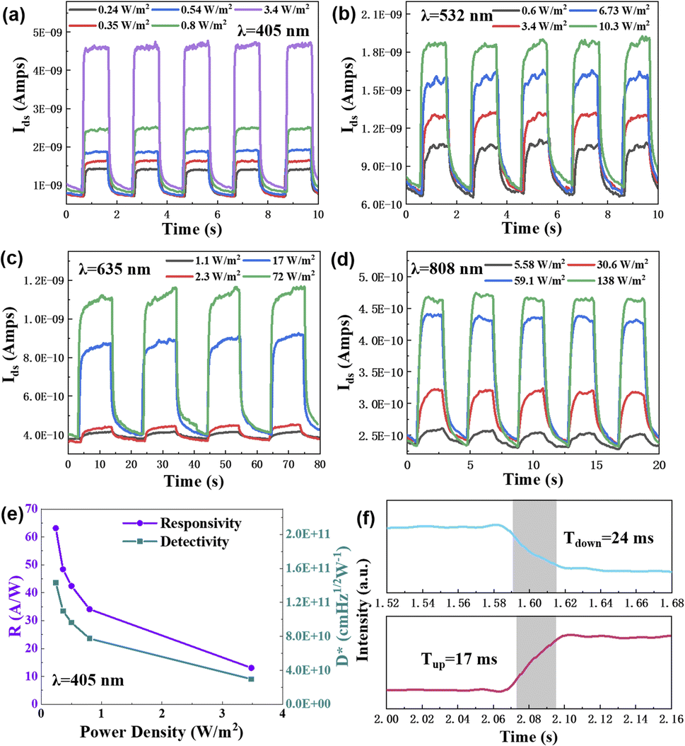 | ||
| Fig. 4 The photoresponse of the Te/SnS2 heterojunction at Vds = 2 V and Vgs = 0 V under the irradiation of (a) 405 nm, (b) 532 nm, (c) 635 nm and (d) 808 nm laser with different light power intensities. (e) The light-power-dependent responsivity and detectivity, and (f) photoresponse time of the Te/SnS2 heterojunction under the irradiation of the 405 nm laser. | ||
The performance of the Te/SnS2 heterojunction was also compared with that of its constituents SnS2 and Te by measuring the photocurrent of the heterojunction and individual materials in the same device. The Te/SnS2 heterojunction has about 1.6-fold improvement in the photocurrent (Fig. S8†) when compared with that of the in-suit SnS2, indicating an improved separation of the photo-induced electron–hole pair in the heterostructure. The Te/SnS2 heterojunction also exhibited an enhancement of about ten times in photoresponsivity when compared with a single SnS2 device with a similar thickness (Fig. S1(d)†). The rising and falling times of the heterojunction and individual material, which are defined as the time for the photocurrent to increase to 90% and decay to 10% of the maximum peak value, were also measured, and the data are shown in Fig. 4(f), S1(d) and S2(d).† The rising and falling time of the heterojunction under the irradiation of 405 nm laser is about 17 and 24 ms, respectively, which is approximately two and three orders of magnitude faster than that of individual SnS2 (1 and 2 s) and Te (10 and 30 s), respectively. The greatly improved response speed may originate from the direct tunneling of the photo-induced carrier at the interface of the device under forward bias. As the band diagram shows in Fig. 3(e), the photo-induced electrons accumulated at the steep potential barrier of the SnS2 side, where the external electric field drags the electrons into Te by direct tunneling. In this way, the electrons recombine quickly with the majority of holes of Te, effectively enhancing the response speed. It is also noticed that the response time increases to subsecond (for 532 and 808 nm) and a few-second (for 635 nm) magnitude when increasing the irradiation wavelength. This special wavelength-dependent response time is probably attributed to the unique charge transfer at the Te/TeO2 hetero-interface of the CVD-growth Te flakes, which we found and discussed in our previous work.32
The photovoltaic characteristics of the tunneling heterojunction were particularly studied. The I–V curve in Fig. 5(a) shows a prominent photocurrent at zero bias when under the irradiation of a 405 nm laser with a power of 0.36 W m−2. The open-circuit voltage Voc and short-circuit current Isc are 0.1 V and 39.7 pA, respectively. Isc and Voc increase with the increase in light power density, as shown in Fig. S9.† The electrical output power Pel is given by the equation
| Pel = VocIsc | (7) |
 | ||
| Fig. 5 The self-power (at zero bias) performance of the Te/SnS2 tunneling heterojunction. (a) Ids–Vds curve under the irradiation of 405 nm laser. The photocurrent in response to the irradiation of (b) 405 nm and (c) 532 nm laser, respectively. (d) The responsivity and detectivity with different light power intensities of 405 nm laser. | ||
The point in the I–V curve that has the maximum electrical output power Pmax can be found in the lower right corner of the blue rectangle in Fig. 5(a). The fill factor (FF) is expressed as
 | (8) |
P max and FF were calculated to be 3.97 pW (at 0.05 V) and 0.25, respectively.
The heterojunction at zero-bias state (Vds = 0 V, Vgs = 0 V) can work in the photovoltaic mode. Fig. 5(b) and (c) show the stable photocurrent of the heterojunction as a self-powered photodetector under irradiation of 405 nm and 532 nm laser. The device also has a response to 635 nm and 808 nm lasers, which is shown in Fig. S10.† Under the irradiation of the 405 nm laser at P = 0.24 W m−2 (Fig. 5(d)), the Rλ, D*, and EQE are calculated to be 2.21 A W−1, 3.55 × 10¹⁰ jones, 678%, respectively, indicating the excellent performance of a self-powered photodetector. By fitting the experimental data, the photocurrent and the optical power density follow the relationship Iph(A) = 6.8 × 10¹¹P0.47, where P is in the unit of W m−2. However, the response speed becomes slower (Fig. S11†) when compared to that at Vds = 2 V. This is probable due to the longer transit time for the carriers to cross the channel as the built-in electric field is much smaller than the external electric field.
To evaluate the self-powered performance of the photodetector based on our Te/SnS2 tunneling heterojunction, we compared the two key parameters of the device with the reported self-powered photodetector based on a tunneling heterojunction, as listed in Table 1. It is obvious that the Rλ of 2.21 A W−1 and EQE of 678% for our device are much higher than those of all the other reported tunneling heterojunctions, showing superior self-powered performance. We also listed the values of many representative high-performance heterojunctions (but not tunneling ones) for comparison. The self-powered performance of our device is very competitive and among one of the best self-powered photodetectors reported so far. Considering the large dark current and ultrafast electron–hole recombination rate originating from the narrow-bandgap materials in the tunneling heterojunction, it is a great challenge to obtain a good self-powered performance in such devices. We believe that the superior self-powered properties of our tunneling heterojunction are attributed to the unique band diagrams of the Te/SnS2 heterostructure. Firstly, as seen in Fig. 3(d), the Ec of SnS2 is positioned in the middle of the forbidden band of Te, which is very close to the Ev of Te (about 0.17 eV). Thus, the generated photo-induced electrons in the on-top Te flakes are easily excited from the Ec of Te to the Ev of SnS2, while the photo-induced holes stay in Te, promoting the separation of electron–hole pairs. Secondly, the Fermi levels of Te and SnS2 have negligible energy differences (0.005 eV), which leads to tiny band bending at the interface of the two materials after contact. Hence, carriers easily transfer from one material to the other due to the very small interfacial potential barrier. The above two features are helpful in the efficient separation of the electron–hole pairs, resulting in excellent photovoltaic properties and self-powered performance.
| Heterojunction | tunneling | Wave length [nm] | Responsivity [mA W−1] | EQE [%] | Ref. |
|---|---|---|---|---|---|
| PtS2/WSe2 | Yes | 635 | 420 | 28 | 20 |
| AsP/InSe | Yes | 520 | 6 | 1.5 | 21 |
| CdS/BP | Yes | 450 | 270 | 76 | 43 |
| WSe2/WSe2 | Yes | 532 | 11.2 | 2.6 | 44 |
| MoS2/WS2 | Yes | 532 | 4.36 | — | 45 |
| Au/InSe/Gr | Yes | 400 | 365 | 46 | |
| PdSe2/MoS2 | No | 532 | 185.6 | 24.5 | 47 |
| MoTe2/MoS2 | No | 520 | 183 | — | 48 |
| Te/WS2 | No | 635 | 471 | 91 | 49 |
| GaTe-MoS2 | No | 514 | 1365 | 266 | 50 |
| WSe2/Bi2O2Se | No | 532 | 284 | 66.3 | 51 |
| Te/Bi2O2Se | No | 532 | 768.8 | — | 52 |
| WSe2/Bi2Te3 | No | 633 | 20500 |
— | 53 |
| Te/Si | No | 808 | 6450 | 998 | 54 |
| Te/SnS2 | Yes | 405 | 2210 | 678 | This work |
Conclusions
In this work, tunneling heterojunctions were fabricated using the stacking of 2D Te and SnS2 flakes. The type-II band alignment of the Te/SnS2 heterojunctions can transfer to type-III one when applying the reverse bias. The Te/SnS2 tunneling heterojunction exhibited a reverse rectification ratio of about 5000. The photodetector based on the heterojunctions shows ultrahigh photoresponsivity 50.5 A W−1 under the irradiation of a 405 nm laser. The heterojunction device exhibits a superior response time of 24 ms, which is approximately two and three orders of magnitude faster than that of individual SnS2 and Te, respectively. Furthermore, the device at zero bias exhibited a high responsivity of 2.21 A W−1 and external quantum efficiency of 678%, which represents one of the best self-powered performances for a heterojunction-based photodetector.Experimental section/methods
Synthesis of Te flakes
The Te flakes were synthesized in a horizontal tube furnace with a single temperature zone by the physical vapor deposition method. Te powder was placed in the centre of the quartz tube and fluorophlogopite mica [KMg3(AlSi3O10)F2] sheets were placed in the downstream area, 14 cm away from the source. The sealed quartz tube was evacuated and flushed a few times with high-purity Ar gas (Xinhe, 99.999%) to provide an oxygen-free environment. The reaction was carried out in the centre of the tube under a constant flow rate of 120 sccm Ar gas at a temperature of 750 °C. The reaction process continued for 15 min followed by natural cooling to room temperature.Preparation of SnS2
SnS2 flakes were exfoliated from the commercial bulk SnS2 (Shanghai Onway, China) using a blue membrane tape (UST, America) and then transferred onto a silicon substrate (with 300 nm SiO2) via PDMS.Device fabrication
After the transfer of the SnS2 flakes onto the SiO2/Si, Te flakes were then transferred from mica to the SnS2/SiO2/Si by polystyrene (PS) to achieve a stacking of Te flakes on the SnS2 ones. Finally, 50 nm-thick Au as an electrode was deposited on the heterojunction through a standard lithography process and thermal evaporation.Characterizations
Morphology, composition, and microstructure of the materials were characterized using optical microscopy (Motic, BA310MET), atomic force microscopy (Bruker, Dimension FastScan), Raman (NOST, FEX, 532 nm excitation laser), transmission electron microscopy (FEI, Thermo, Talos F200S), X-ray diffraction (Bruker, D8 VENTURE) and X-ray photoelectron spectroscopy (Thermo Fisher, Escalab 250Xi) techniques. The photoresponse properties of the devices were studied on a four-probe system (Semishare SM-4, China) combined with a 2636B source meter (KEITHLEY, America). The photodetectors were measured under 405, 532, 635, and 808 nm lasers in the air at room temperature.Author contributions
Yu Zhao: conceptualization, methodology, formal analysis, data curation, resources, funding acquisition, and writing–original draft. Xuanhao Cao: conceptualization, methodology, investigation, data curation, and writing-original draft. Zehong Lei: investigation, and data curation. Lili Tao, Zhaoqiang Zheng, Xing Feng: formal analysis, and writing–review and editing. Jingbo Li: supervision, and funding acquisition. All authors have discussed the results of this manuscript. All authors have given approval for the final version of the manuscript.Conflicts of interest
There are no conflicts to declare.Acknowledgements
This work was sponsored by the National Natural Science Foundation of China (Grant no. 61975036), the Fund of Guangdong Provincial Key Laboratory of Information Photonics Technology (Grant no. 2020B121201011) and the Pearl River Talent Recruitment Program (Grant no. 2019ZT08X639).References
- K. S. Novoselov, A. Mishchenko, A. Carvalho and A. H. Castro Neto, Science, 2016, 353, aac9439 CrossRef CAS PubMed.
- X. Duan, C. Wang, A. Pan, R. Yu and X. Duan, Chem. Soc. Rev., 2015, 44, 8859–8876 RSC.
- W. Hu and J. Yang, J. Mater. Chem. C, 2017, 5, 12289–12297 RSC.
- X. Cao, Z. Lei, B. Huang, A. Wei, L. Tao, Y. Yang, Z. Zheng, X. Feng, J. Li and Y. Zhao, Small, 2022, 18, 2200445 CrossRef CAS PubMed.
- D. Unuchek, A. Ciarrocchi, A. Avsar, K. Watanabe, T. Taniguchi and A. Kis, Nature, 2018, 560, 340–344 CrossRef CAS PubMed.
- Y. Shimazaki, I. Schwartz, K. Watanabe, T. Taniguchi, M. Kroner and A. Imamoğlu, Nature, 2020, 580, 472–477 CrossRef CAS PubMed.
- A. Du, S. Sanvito, Z. Li, D. Wang, Y. Jiao, T. Liao, Q. Sun, Y. H. Ng, Z. Zhu, R. Amal and S. C. Smith, J. Am. Chem. Soc., 2012, 134, 4393–4397 CrossRef CAS PubMed.
- M. M. Otrokov, I. I. Klimovskikh, H. Bentmann, D. Estyunin, A. Zeugner, Z. S. Aliev, S. Gaß, A. U. B. Wolter, A. V. Koroleva, A. M. Shikin, M. Blanco-Rey, M. Hoffmann, I. P. Rusinov, A. Y. Vyazovskaya, S. V. Eremeev, Y. M. Koroteev, V. M. Kuznetsov, F. Freyse, J. Sánchez-Barriga, I. R. Amiraslanov, M. B. Babanly, N. T. Mamedov, N. A. Abdullayev, V. N. Zverev, A. Alfonsov, V. Kataev, B. Büchner, E. F. Schwier, S. Kumar, A. Kimura, L. Petaccia, G. Di Santo, R. C. Vidal, S. Schatz, K. Kißner, M. Ünzelmann, C. H. Min, S. Moser, T. R. F. Peixoto, F. Reinert, A. Ernst, P. M. Echenique, A. Isaeva and E. V. Chulkov, Nature, 2019, 576, 416–422 CrossRef CAS PubMed.
- S. Kezilebieke, M. N. Huda, V. Vaňo, M. Aapro, S. C. Ganguli, O. J. Silveira, S. Głodzik, A. S. Foster, T. Ojanen and P. Liljeroth, Nature, 2020, 588, 424–428 CrossRef CAS PubMed.
- K. Zhang, T. Zhang, G. Cheng, T. Li, S. Wang, W. Wei, X. Zhou, W. Yu, Y. Sun, P. Wang, D. Zhang, C. Zeng, X. Wang, W. Hu, H. J. Fan, G. Shen, X. Chen, X. Duan, K. Chang and N. Dai, ACS Nano, 2016, 10, 3852–3858 CrossRef CAS PubMed.
- T. Yang, B. Zheng, Z. Wang, T. Xu, C. Pan, J. Zou, X. Zhang, Z. Qi, H. Liu, Y. Feng, W. Hu, F. Miao, L. Sun, X. Duan and A. Pan, Nat. Commun., 2017, 8, 1906 CrossRef PubMed.
- F. Wang, Z. Wang, K. Xu, F. Wang, Q. Wang, Y. Huang, L. Yin and J. He, Nano Lett., 2015, 15, 7558–7566 CrossRef CAS PubMed.
- X. Zhou, X. Hu, S. Zhou, H. Song, Q. Zhang, L. Pi, L. Li, H. Li, J. Lü and T. Zhai, Adv. Mater., 2018, 30, 1703286 CrossRef.
- S. Li, W. Zang, X. Liu, S. J. Pennycook, Z. Kou, C. Yang, C. Guan and J. Wang, Chem. Eng. J., 2019, 359, 1419–1426 CrossRef CAS.
- J. Ran, W. Guo, H. Wang, B. Zhu, J. Yu and S.-Z. Qiao, Adv. Mater., 2018, 30, 1800128 CrossRef PubMed.
- O. Lopez-Sanchez, E. Alarcon Llado, V. Koman, A. Fontcuberta i Morral, A. Radenovic and A. Kis, ACS Nano, 2014, 8, 3042–3048 CrossRef CAS PubMed.
- Y. Xue, Y. Zhang, Y. Liu, H. Liu, J. Song, J. Sophia, J. Liu, Z. Xu, Q. Xu, Z. Wang, J. Zheng, Y. Liu, S. Li and Q. Bao, ACS Nano, 2016, 10, 573–580 CrossRef CAS PubMed.
- L. Ye, H. Li, Z. Chen and J. Xu, ACS Photonics, 2016, 3, 692–699 CrossRef CAS.
- L. Tao, B. Yao, Q. Yue, Z. Dan, P. Wen, M. Yang, Z. Zheng, D. Luo, W. Fan, X. Wang and W. Gao, Nanoscale, 2021, 13, 15403–15414 RSC.
- C. Tan, S. Yin, J. Chen, Y. Lu, W. Wei, H. Du, K. Liu, F. Wang, T. Zhai and L. Li, ACS Nano, 2021, 15, 8328–8337 CrossRef CAS PubMed.
- F. Wu, H. Xia, H. Sun, J. Zhang, F. Gong, Z. Wang, L. Chen, P. Wang, M. Long, X. Wu, J. Wang, W. Ren, X. Chen, W. Lu and W. Hu, Adv. Funct. Mater., 2019, 29, 1900314 CrossRef.
- P. K. Srivastava, Y. Hassan, Y. Gebredingle, J. Jung, B. Kang, W. J. Yoo, B. Singh and C. Lee, ACS Appl. Mater. Interfaces, 2019, 11, 8266–8275 CrossRef CAS PubMed.
- X. Yan, C. Liu, C. Li, W. Bao, S. Ding, D. W. Zhang and P. Zhou, Small, 2017, 13, 1701478 CrossRef.
- H. Qiao, Z. Huang, X. Ren, S. Liu, Y. Zhang, X. Qi and H. Zhang, Adv. Opt. Mater., 2020, 8, 1900765 CrossRef CAS.
- Y. Zhang, W. Xu, X. Xu, W. Yang, S. Li, J. Chen and X. Fang, Nanoscale Horiz., 2019, 4, 452 RSC.
- X. Xu, J. Chen, S. Cai, Z. Long, Y. Zhang, L. Su, S. He, C. Tang, P. Liu, H. Peng and X. Fang, Adv. Mater., 2018, 30, 1803165 CrossRef PubMed.
- Z. Zhang, Y. Ning and X. Fang, J. Mater. Chem. C, 2019, 7, 223 RSC.
- W. Song, J. Chen, Z. Li and X. Fang, Adv. Mater., 2021, 33, 2101059 CrossRef CAS PubMed.
- M. Peng, Y. Yu, Z. Wang, X. Fu, Y. Gu, Y. Wang, K. Zhang, Z. Zhang, M. Huang, Z. Cui, F. Zhong, P. Wu, J. Ye, T. Xu, Q. Li, P. Wang, F. Yue, F. Wu, J. Dai, C. Chen and W. Hu, ACS Photonics, 2022, 9, 1775–1782 CrossRef CAS.
- M. Peng, R. Xie, Z. Wang, P. Wang, F. Wang, H. Ge, Y. Wang, F. Zhong, P. Wu, J. Ye, Q. Li, L. Zhang, X. Ge, Y. Ye, Y. Lei, W. Jiang, Z. Hu, F. Wu, X. Zhou, J. Miao, J. Wang, H. Yan, C. Shan, J. Dai, C. Chen, X. Chen, W. Lu and W. Hu, Sci. Adv., 2021, 7, eabf7358 CrossRef CAS PubMed.
- Z. Shi, R. Cao, K. Khan, A. K. Tareen, X. Liu, W. Liang, Y. Zhang, C. Ma, Z. Guo, X. Luo and H. Zhang, Nano-Micro Lett., 2020, 12, 99 CrossRef CAS PubMed.
- B. Huang, Z. Lei, X. Cao, A. Wei, L. Tao, Y. Yang, J. Liu, Z. Zheng and Y. Zhao, J. Mater. Chem. C, 2021, 9, 14394–14400 RSC.
- G. Domingo, R. S. Itoga and C. R. Kannewurf, Phys. Rev., 1966, 143, 536–541 CrossRef CAS.
- Y. Hu, T. Chen, X. Wang, L. Ma, R. Chen, H. Zhu, X. Yuan, C. Yan, G. Zhu, H. Lv, J. Liang, Z. Jin and J. Liu, Nano Res., 2017, 10, 1434–1447 CrossRef CAS.
- L. Xu, P. Zhang, H. Jiang, X. Wang, F. Chen, Z. Hu, Y. Gong, L. Shang, J. Zhang, K. Jiang and J. Chu, Small, 2019, 15, 1904116 CrossRef CAS PubMed.
- J. Peng, Y. Pan, Z. Yu, J. Wu, J. Wu, Y. Zhou, Y. Guo, X. Wu, C. Wu and Y. Xie, Angew. Chem., Int. Ed., 2018, 57, 13533–13537 CrossRef CAS PubMed.
- Y. Wang, G. Qiu, R. Wang, S. Huang, Q. Wang, Y. Liu, Y. Du, W. A. Goddard, M. J. Kim, X. Xu, P. D. Ye and W. Wu, Nat. Electron., 2018, 1, 228–236 CrossRef.
- G. Su, V. G. Hadjiev, P. E. Loya, J. Zhang, S. Lei, S. Maharjan, P. Dong, P. M. Ajayan, J. Lou and H. Peng, Nano Lett., 2015, 15, 506–513 CrossRef CAS.
- A. Coker, T. Lee and T. P. Das, Phys. Rev. B: Condens. Matter Mater. Phys., 1980, 22, 2968–2975 CrossRef CAS.
- K. Murali, M. Dandu, S. Das and K. Majumdar, ACS Appl. Mater. Interfaces, 2018, 10, 5657–5664 CrossRef CAS PubMed.
- L. Liu, C. Liu, X. Huang, S. Zeng, Z. Tang, D. W. Zhang and P. Zhou, Adv. Electron. Mater., 2022, 8, 2100869 CrossRef CAS.
- S. M. Sze and K. K. Ng, Physics of Semiconductor Devices, John Wiley & Sons, Hoboken, New Jersey, USA, 2006 Search PubMed.
- M. Zubair, C. Zhu, X. Sun, H. Liu, B. Zheng, J. Yi, X. Zhu, D. Li and A. Pan, Sci. China Mater., 2020, 63, 1570–1578 CrossRef CAS.
- C. Tan, H. Wang, X. Zhu, W. Gao, H. Li, J. Chen, G. Li, L. Chen, J. Xu, X. Hu, L. Li and T. Zhai, ACS Appl. Mater. Interfaces, 2020, 12, 44934–44942 CrossRef CAS.
- W. Wu, Q. Zhang, X. Zhou, L. Li, J. Su, F. Wang and T. Zhai, Nano Energy, 2018, 51, 45–53 CrossRef CAS.
- M. Dai, H. Chen, F. Wang, M. Long, H. Shang, Y. Hu, W. Li, C. Ge, J. Zhang, T. Zhai, Y. Fu and P. Hu, ACS Nano, 2020, 14, 9098–9106 CrossRef CAS PubMed.
- M. Long, Y. Wang, P. Wang, X. Zhou, H. Xia, C. Luo, S. Huang, G. Zhang, H. Yan, Z. Fan, X. Wu, X. Chen, W. Lu and W. Hu, ACS Nano, 2019, 13, 2511–2519 CAS.
- S. Li, Z. He, Y. Ke, J. Guo, T. Cheng, T. Gong, Y. Lin, Z. Liu, W. Huang and X. Zhang, Appl. Phys. Express, 2019, 13, 015007 CrossRef.
- L. Han, M. Yang, P. Wen, W. Gao, N. Huo and J. Li, Nanoscale Adv., 2021, 3, 2657–2665 RSC.
- S. Yang, C. Wang, C. Ataca, Y. Li, H. Chen, H. Cai, A. Suslu, J. C. Grossman, C. Jiang, Q. Liu and S. Tongay, ACS Appl. Mater. Interfaces, 2016, 8, 2533–2539 CrossRef CAS.
- P. Luo, F. Wang, J. Qu, K. Liu, X. Hu, K. Liu and T. Zhai, Adv. Funct. Mater., 2021, 31, 2008351 CrossRef CAS.
- W. Wang, Y. Meng, W. Wang, Z. Zhang, P. Xie, Z. Lai, X. Bu, Y. Li, C. Liu, Z. Yang, S. Yip and J. C. Ho, Adv. Funct. Mater., 2022, 2203003 CrossRef CAS.
- H. Liu, X. Zhu, X. Sun, C. Zhu, W. Huang, X. Zhang, B. Zheng, Z. Zou, Z. Luo, X. Wang, D. Li and A. Pan, ACS Nano, 2019, 13, 13573–13580 CrossRef CAS PubMed.
- T. Zheng, M. Yang, Y. Sun, L. Han, Y. Pan, Q. Zhao, Z. Zheng, N. Huo, W. Gao and J. Li, J. Mater. Chem. C, 2022, 10, 7283–7293 RSC.
Footnote |
| † Electronic supplementary information (ESI) available. See https://doi.org/10.1039/d2na00507g |
| This journal is © The Royal Society of Chemistry 2022 |