DOI:
10.1039/D2NA00623E
(Paper)
Nanoscale Adv., 2022,
4, 5144-5153
Giant tunneling magnetoresistance in two-dimensional magnetic tunnel junctions based on double transition metal MXene ScCr2C2F2†
Received
14th September 2022
, Accepted 22nd October 2022
First published on 24th October 2022
Abstract
Two-dimensional (2D) transition metal carbides (MXenes) with intrinsic magnetism and half-metallic features show great promising applications for spintronic and magnetic devices, for instance, achieving perfect spin-filtering in van der Waals (vdW) magnetic tunnel junctions (MTJs). Herein, combining density functional theory calculations and nonequilibrium Green's function simulations, we systematically investigated the spin-dependent transport properties of 2D double transition metal MXene ScCr2C2F2-based vdW MTJs, where ScCr2C2F2 acts as the spin-filter tunnel barriers, 1T-MoS2 acts as the electrode and 2H-MoS2 as the tunnel barrier. We found that the spin-up electrons in the parallel configuration state play a decisive role in the transmission behavior. We found that all the constructed MTJs could hold large tunnel magnetoresistance (TMR) ratios over 9 × 10⁵%. Especially, the maximum giant TMR ratio of 6.95 × 10⁶% can be found in the vdW MTJ with trilayer 2H-MoS2 as the tunnel barrier. These results indicate the potential for spintronic applications of vdW MTJs based on 2D double transition metal MXene ScCr2C2F2.
Introduction
A magnetic tunnel junction (MTJ) is an important spintronic device, which consists of two ferromagnets divided by a thin insulating barrier.1,2 MTJs are widely utilized in magnetic random-access memory, hard disks, and magnetic sensors, etc.3–6 Furthermore, much efforts have been put into the relevant research for MTJs since the tunneling magnetoresistance (TMR) effect was firstly discovered in Fe/Ge/Co multilayer films.7–9 Herein, the TMR ratio is regarded as one of the most important factors for estimating the performance of MTJs. To enhance the TMR ratio, an effective method involves employing intrinsic magnetic materials with high spin polarizabilities as the electrode material.10,11 In early years, three-dimensional (3D) magnetic metals such as Fe, Ni, and Co are employed as the ferromagnetic electrodes in MTJs.12 Unfortunately, the limited spin polarizations lower than 50% result in low TMR ratios for these 3D magnetic metals.13–15 It is interesting to note that the TMR ratios of MTJs could be improved to a higher level by employing half-metallic (HM) materials as electrodes.16–18 This is because HM materials possess 100% spin polarization theoretically.19 However, controlling the quality of the interface between the electrode materials and barrier layers is one of the thorny challenges in 3D HM material-based MTJs.20 When constructing the MTJs by cleaving 3D materials, the surface dangling bonds will inevitably cause atomic distortion, disorder, and point defects, which could strengthen the interfacial scattering, and lead to the reduction of the TMR ratio.21
Recently, the successful synthesis of intrinsic magnetic two-dimensional (2D) materials, such as CrI3,22 Cr2Ge2Te6,23 and Fe3GeTe2,24 has opened a new horizon for spintronic devices. Constructing van der Waals (vdW) MTJs via perpendicularly stacking magnetic and dielectric 2D materials together through vdW interactions offers impressive performance with high TMR ratios.25 For example, a TMR ratio of 160% has been experimentally obtained in Fe3GeTe2|h-BN|Fe3GeTe2 vdW MTJs at low temperatures.26 Moreover, the TMR ratio of graphene/CrI3/graphene vdW MTJ up to 19![[thin space (1/6-em)]](https://www.rsc.org/images/entities/char_2009.gif) 000% has been experimentally realized by increasing the CrI3 layer thickness.27 It is theoretically predicted that a giant zero-bias TMR ratio of up to 48
000% has been experimentally realized by increasing the CrI3 layer thickness.27 It is theoretically predicted that a giant zero-bias TMR ratio of up to 48![[thin space (1/6-em)]](https://www.rsc.org/images/entities/char_2009.gif) 000% can be achieved using CrOCl/CrOX bilayer as the spin-filter tunnel barriers.28 On the other hand, the vdW MTJs based on 1T-VSe2 possess a high TMR ratio of 5600%, and the TMR ratio is sharply increased to 1.7 × 10⁵% by inserting 2H-MoSe2.29 Two kinds of 6,6,12-graphyne-based molecular magnetic tunnel junctions have novel transport behaviors, and the maximum order of magnitude of tunneling magnetoresistance values reaches 106%.30 Wang et al. reported the spin-dependent transport properties of a molecular junction made of two manganese phthalocyanine molecules linked by single-walled carbon nanotubes and predicted a high spin-filter efficiency and magnetoresistance ratio.31 However, it is still challenging to develop 2D materials with intrinsic magnetism to achieve giant TMR ratios in MTJs.
000% can be achieved using CrOCl/CrOX bilayer as the spin-filter tunnel barriers.28 On the other hand, the vdW MTJs based on 1T-VSe2 possess a high TMR ratio of 5600%, and the TMR ratio is sharply increased to 1.7 × 10⁵% by inserting 2H-MoSe2.29 Two kinds of 6,6,12-graphyne-based molecular magnetic tunnel junctions have novel transport behaviors, and the maximum order of magnitude of tunneling magnetoresistance values reaches 106%.30 Wang et al. reported the spin-dependent transport properties of a molecular junction made of two manganese phthalocyanine molecules linked by single-walled carbon nanotubes and predicted a high spin-filter efficiency and magnetoresistance ratio.31 However, it is still challenging to develop 2D materials with intrinsic magnetism to achieve giant TMR ratios in MTJs.
Among various 2D materials, 2D transition metal carbides/nitrides (MXene) materials have attracted much attention due to their fascinating tunable physical and chemical properties from the remarkable variety of chemical diversity.32–34 MXenes have a general formula of Mn+1XnTx, where M, X, and T represent early transition metals, carbon/nitrogen, and the functional groups (such as O, OH, and F), respectively.35 It is worth noting that MXene Cr2C without the surface functional groups is predicted to have intrinsic half-metallicity, and ferromagnetic to antiferromagnetic transitions accompanied by metal-to-insulator transitions can be observed after adsorbing different surface functional groups.36 Moreover, some intrinsic magnetic MXenes, such as Cr2NX2 (X = O, F, OH),37 Mn2CT2 (T = F, Cl, OH, O, and H)38 are found to possess HM polarization nature and are proposed as potential candidates for vdW MTJs or spin filters.39,40 Apart from that, double transition metal (DTM) MXenes, including two different transition metals with the general formula of  41,42 offer more possibilities for fantastic magnetic properties.43–45 Recently, impressive intrinsic magnetic properties have been found in HM DTM MXenes, such as ScCr2C2F2, ZrCr2C2H2 and YCr2C2H2.46 Herein, ScCr2C2F2 presents a high Curie temperature of 230 K based on the Metropolis Monte Carlo (MC) simulations. Although TC could be theoretically overestimated, recently good agreement between theoretical results and experimental values have been achieved, for instance, in the case of CrI3 and Fe3GeTe2.46,47 The MC predicted TC of 230 K indicates that ScCr2C2F2 is anticipated to achieve distinguished MTJ performance as the ferromagnetic electrodes. Therefore, a systematical understanding and optimization of ScCr2C2F2-based vdW MTJs are of great interest and importance.
In this work, by employing ScCr2C2F2 as the spin-filter tunnel barriers, 1T-MoS2 and 2H-MoS2 respectively, as the electrode and tunnel barrier, we have designed and optimized the 1T-MoS2/ScCr2C2F2/2H-MoS2/ScCr2C2F2/1T-MoS2 vdW MTJs with different stacking configurations and tunnel barrier layer numbers. The interlayer charge transfers, spin-dependent transmission coefficients, spectra projected local density of states, and TMR ratios in the equilibrium state of the constructed vdW MTJs were investigated. The negative binding and formation energies of ScCr2C2F2/1T-MoS2 and ScCr2C2F2/2H-MoS2 heterostructures demonstrate that different layers could stack spontaneously in experiments. Besides, the energetically favorable stacking-II of the ScCr2C2F2/1T-MoS2 interface and stacking-I configurations for the ScCr2C2F2/1T-MoS2 interface are selected to construct the vdW MTJs, which will increase the experimental feasibility. Furthermore, it reveals that the monolayer ScCr2C2F2 can maintain half-metallicity with perfect polarization after application in the vdW MTJs. Large TMR ratios of over 9 × 10⁵% are found in all the constructed vdW MTJs, and the maximum TMR ratio of 6.95 × 10⁶% was detected in such vdW MTJ with a trilayer 2H-MoS2 tunnel barrier. Our findings demonstrate that such DTM MXene-based vdW MTJs have application potential in spintronics.
Computational methods
In order to obtain the interlayer structures before modeling the vdW MTJs, the different stacking configurations for ScCr2C2F2/1T-MoS2 and ScCr2C2F2/2H-MoS2 heterostructures were built using the ALKEMIE platform,48,49 and investigated based on the density functional theory (DFT) calculations using the Vienna Ab initio Simulation Package (VASP).50 The generalized gradient approximation (GGA) with Perdew–Burke–Ernzerhof (PBE)51 was used for the exchange and correlation potentials. To better describe the correlation effect of localized 3d electrons in Cr atoms, the GGA + U method with the on-site effective interaction parameter U = 3.0 eV was used.52 The plane-wave cut-off energy of 500 eV and 12 × 12 × 1 K-points were utilized for the optimization and self-consistent calculations. The DFT-D3 method53,54 was adopted to describe the interlayer van der Waals force. To avoid the interlayer interaction, a 20 Å vacuum was added on top of the 2D materials. The heterostructures were relaxed with the convergence energy for electrons and convergence forces for atoms to 1 × 10⁻⁵ eV and 0.01 eV Å−1, respectively.
The optimizations and spin-dependent transport calculations of vdW MTJs were implemented using the QuantumWise Atomistix Toolkit (QuantumATK) Q-2021.06 package,55 based on DFT combined with the nonequilibrium Green's function (NEGF).56 The generalized gradient approximation (GGA) of the Perdew–Burke–Ernzerhof (PBE)51 functional with a linear combination of atomic orbitals (LCAO) norm-conserving PseudoDojo pseudopotential57 were included to deal with the electron exchange and correctional interactions. The double-zeta basis set used to expand wave functions was employed for the calculations.58 The plane-wave cut-off of 105 Hartree was employed, 10 × 10 × 1 Monkhorst k-point meshes were used for the optimization of the MTJs before performing the spin-dependent transport calculations, and the convergence criterion of the force was set to 0.01 eV Å−1. The electron temperature was set at 300 K, which was determined by the Fermi–Dirac distribution via the occupation number of each state. When performing the self-consistent calculation, 10 × 10 × 1 Monkhorst k-point meshes were utilized for the central scattering regions. Besides, inspired by the set of electrodes of the recently proposed NiI2/In2Se3 multiferroic devices,59 the dense enough k-points set was required for the electrodes along the transport direction since they are regarded as the periodic bulk structures for the transport calculations. The Monkhorst k-point meshes for the electrodes were set to 10 × 10 × 150, which is dense enough to ensure the accuracy of the results, and 151 × 151 Monkhorst–Pack grids were used for the spin-dependent transport calculations.
Results and discussion
In 1T-MoS2/ScCr2C2F2/2H-MoS2/ScCr2C2F2/1T-MoS2 vdW MTJs, the origin of TMR effects arise from the different densities of states for spin-up and spin-down channels of the ScCr2C2F2 layers, which act as the spin-filter tunnel barriers. The corresponding transportation mechanism is illustrated in Fig. 1. When the external magnetic fields are applied in vdW MTJs, the magnetic configurations of the two ScCr2C2F2 layers are manipulated to parallel configuration (PC) and antiparallel configuration (APC) states, individually. The tunneling resistances in vdW MTJs vary widely varied in PC and APC. Herein, the TMR ratio is the most important factor in estimating the performance of the magnetic tunnel junctions, which is defined as60| |  | (1) |
where RAPC and RPC are the tunneling resistances in PC and APC, respectively. P1 and P2 represent the spin polarization of the left and right ferromagnetic materials, respectively. When the device is in the PC state, the spin-up electrons from the left 1T-MoS2 electrode can hop to the spin-up states around the Fermi level in the left ScCr2C2F2 layer, which can further go through the 2H-MoS2 barrier layer due to the quantum tunneling effect. Subsequently, the spin-up electrons around the Fermi level can hop to the spin-up states of the right ScCr2C2F2 layer, and finally hop to the spin-up states of the right 1T-MoS2 electrode. However, owing to the semiconducting feature of the left ScCr2C2F2 in the spin-down channel, a rare state is observed around the Fermi level. Hence, the spin-down electrons from the left 1T-MoS2 electrode cannot hop to the spin-down states of the left ScCr2C2F2 layer. As a result, the vdW MTJ is in a high conductivity state with the contribution of the conductive spin-up electron channel. When the device is in the APC state, both the spin-up and spin-down electrons can hardly pass through the vdW MTJ since the spin-up and spin-down electrons are prevented from hopping to the left and right ScCr2C2F2 layers, respectively. As a result, the vdW MTJ is in a high resistance state. Therefore, a considerable difference in the tunneling resistances is obtained from the 1T-MoS2/ScCr2C2F2/2H-MoS2/ScCr2C2F2/1T-MoS2 vdW MTJ with different spin configurations, where the high conductivity PC state and high resistance APC state are regarded as “1” and “0” states for data storage.61,62
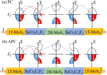 |
| | Fig. 1 The electron tunneling mechanism of the 1T-MoS2/ScCr2C2F2/2H-MoS2/ScCr2C2F2/1T-MoS2 MTJ in (a) PC and (b) APC states. | |
The crystal structures of ScCr2C2F2, 1T-MoS2 and 2H-MoS2 monolayers are shown in Fig. 2a–c. Herein, ScCr2C2F2 and 1T-MoS2 have hexagonal crystal structures with the space group of P![[3 with combining macron]](https://www.rsc.org/images/entities/char_0033_0304.gif) m1, and 2H-MoS2 has the space group of P
m1, and 2H-MoS2 has the space group of P![[6 with combining macron]](https://www.rsc.org/images/entities/char_0036_0304.gif) m2. The optimized lattice constant of ScCr2C2F2 is 3.12 Å. The optimized lattice constants of both 1T-MoS2 and 2H-MoS2 are 3.18 Å, which not only agrees well with the experimental values,63–66 but also exhibits a perfect lattice match with ScCr2C2F2. Fig. 2d and f illustrates the calculated band structures for ScCr2C2F2, 1T-MoS2, and 2H-MoS2 monolayers. From Fig. 2d, ScCr2C2F2 shows the metallic properties in the spin-up channel and semiconducting properties in the spin-down channel, revealing its half-metallic magnetic features. On the other hand, from Fig. 2e and f, 1T-MoS2 and 2H-MoS2 are demonstrated to be metallic conducting and semiconducting, respectively. Therefore, 1T-MoS2 and 2H-MoS2 could be employed as the electrodes and tunnel barrier for the vdW MTJs.
m2. The optimized lattice constant of ScCr2C2F2 is 3.12 Å. The optimized lattice constants of both 1T-MoS2 and 2H-MoS2 are 3.18 Å, which not only agrees well with the experimental values,63–66 but also exhibits a perfect lattice match with ScCr2C2F2. Fig. 2d and f illustrates the calculated band structures for ScCr2C2F2, 1T-MoS2, and 2H-MoS2 monolayers. From Fig. 2d, ScCr2C2F2 shows the metallic properties in the spin-up channel and semiconducting properties in the spin-down channel, revealing its half-metallic magnetic features. On the other hand, from Fig. 2e and f, 1T-MoS2 and 2H-MoS2 are demonstrated to be metallic conducting and semiconducting, respectively. Therefore, 1T-MoS2 and 2H-MoS2 could be employed as the electrodes and tunnel barrier for the vdW MTJs.
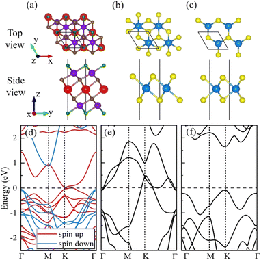 |
| | Fig. 2 The crystal structures and band structures for monolayers of (a) and (d) ScCr2C2F2, (b) and (e) 1T-MoS2, (c) and (f) 2H-MoS2. | |
In 1T-MoS2/ScCr2C2F2/2H-MoS2/ScCr2C2F2/1T-MoS2 vdW MTJs, there are two important vdW interfaces: the ScCr2C2F2/1T-MoS2 interface and the ScCr2C2F2/2H-MoS2 interface. To find the stable interfacial connections in the vdW MTJs, we investigated the different stacking configurations of ScCr2C2F2/1T-MoS2 and ScCr2C2F2/2H-MoS2 heterostructures. As depicted in Fig. 3, each of them owns six different possible stacking configurations. For stacking-I of ScCr2C2F2/1T-MoS2 heterostructure, the Mo atoms of the 1T-MoS2 layer lie on top of the upper F atoms of the ScCr2C2F2 layer, and the upper Cr and C atoms sit right across the upper and bottom S atoms, respectively. Stacking-II and stacking-III are obtained from stacking-I by shifting the 1T-MoS2 layer along the [110] direction of 1/3 and 2/3a, respectively. For stacking-IV, the Mo atoms of the 1T-MoS2 layer lie on top of the Sc atoms and upper F atoms of the ScCr2C2F2 layer, and the upper Cr and C atoms sit right from the bottom and upper S atoms, respectively. Similarly, stacking-V and stacking-VI are obtained from stacking-IV by shifting the 1T-MoS2 layer along the [110] direction of 1/3 and 2/3a, respectively. For stacking-I of ScCr2C2F2/2H-MoS2 heterostructure, the Mo atoms of the 2H-MoS2 layer lie on top of the upper C atoms, and the S atoms sit right across the upper Cr atoms. For stacking-IV of ScCr2C2F2/2H-MoS2 heterostructures, the Mo atoms of the 2H-MoS2 layer lie on top of the upper Cr atoms, and the S atoms sit right across the upper C atoms. The transition of ScCr2C2F2/2H-MoS2 heterostructures from stacking-I to stacking-II/stacking-III and from stacking-IV to stacking-V/stacking-VI is the same as that in the ScCr2C2F2/1T-MoS2 heterostructure.
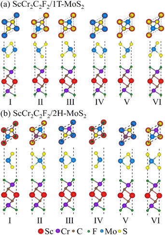 |
| | Fig. 3 The structure schematic diagrams of (a) ScCr2C2F2/1T-MoS2 heterostructure and (b) ScCr2C2F2/2H-MoS2 heterostructure with different stacking configurations. | |
To estimate the stabilities of the different stacking configurations, the binding energies (Ebind) and formation energies (Eform) were calculated using the following equations67,68
| |  | (2) |
| | | Eform = EScCr2C2F2/MoS2 − EScCr2C2F2 − EMoS2 | (3) |
where
EScCr2C2F2/MoS2is the total energy of the ScCr
2C
2F
2/1T-MoS
2 (or ScCr
2C
2F
2/2H-MoS
2) heterostructures,

stand for the total energies of ScCr
2C
2F
2 and 1T-MoS
2 (or 2H-MoS
2) monolayers constrained in the corresponding heterostructure lattice, respectively.
S is the interface area.
EScCr2C2F2 and
EMoS2 represent the free-standing total energies of ScCr
2C
2F
2 and 1T-MoS
2 (or 2H-MoS
2) monolayers. The calculated
Ebind and
Eform are summarized in
Table 1. The negative
Ebind and
Eform demonstrate that all the stacking configurations of ScCr
2C
2F
2/1T-MoS
2 and ScCr
2C
2F
2/2H-MoS
2 heterostructures can form spontaneously. It is worth noting that the stacking-II of ScCr
2C
2F
2/1T-MoS
2 heterostructure and stacking-I of ScCr
2C
2F
2/1T-MoS
2 heterostructure are more favorable to exist in experiments due to their lowest
Ebind and
Eform among various stacking configurations in
Table 1. Based on the
Ebind and
Eform results, energetically-favorable stacking-II for the ScCr
2C
2F
2/1T-MoS
2 interface and stacking-I configurations for the ScCr
2C
2F
2/1T-MoS
2 interface were selected to construct the vdW MTJs.
Table 1 Formation energies Eform (meV) and binding energies Ebind (meV Å−2) of different stacking configurations of ScCr2C2F2/1T-MoS2 and ScCr2C2F2/1T-MoS2 heterostructures
| Stacking |
ScCr2C2F2/1T-MoS2 |
ScCr2C2F2/2H-MoS2 |
|
E
form
|
E
bind
|
E
form
|
E
bind
|
| I |
−247.46 |
−29.88 |
−208.23 |
−25.15 |
| II |
−255.79 |
−30.91 |
−152.59 |
−18.69 |
| III |
−193.68 |
−23.43 |
−152.39 |
−18.65 |
| IV |
−250.63 |
−30.24 |
−201.82 |
−24.47 |
| V |
−251.70 |
−30.48 |
−204.12 |
−24.64 |
| VI |
−193.92 |
−23.44 |
−199.54 |
−24.15 |
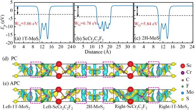
The work function (WG) and charge transfer between different materials in the MTJ could strongly influence the interfacial effects and the devices' performance.69,70 To further understand the interfacial effects in the 1T-MoS2/ScCr2C2F2/2H-MoS2/ScCr2C2F2/1T-MoS2 vdW MTJ, we calculated the electrostatic potential for the 1T-MoS2, 2H-MoS2 and ScCr2C2F2 monolayers, as shown in Fig. 4a–c, respectively. The work function is defined as the difference between the vacuum energy level and the Fermi level of a 2D material. As depicted in Fig. 4a–c, the values of WG for 1T-MoS2, 2H-MoS2, and ScCr2C2F2 monolayers are 5.06, 5.84, and 6.78 eV, respectively. When two different 2D materials are in contact, the electrons of the lower work function side will flow to the higher work function side until their Fermi levels are equal.71 Therefore, the interlayer charge transfers from 1T-MoS2/2H-MoS2 to ScCr2C2F2 layers are inferred due to the difference in work functions. To verify the corollary, the charge redistributions in the corresponding 1T-MoS2/ScCr2C2F2/2H-MoS2/ScCr2C2F2/1T-MoS2 heterostructure are represented from the differential charge density plots in Fig. 4d and e. As seen in the interfacial regions marked with magenta dashed boxes, charge accumulations occur at the F terminations in the ScCr2C2F2 layers, and charge depletions are found at the S terminations in the 1T-MoS2 and 2H-MoS2 layers.
 |
| | Fig. 4 The electrostatic potential Ep for (a) 1T-MoS2, (b) monolayer ScCr2C2F2 and (c) 2H-MoS2. The differential charge density of 1T-MoS2/ScCr2C2F2/2H-MoS2/ScCr2C2F2/1T-MoS2 heterostructure in (d) PC and (e) APC states. The isosurface value is set to 0.0002 e bohr−1,3 and the yellow and cyan regions represent the accumulation and depletion of electrons, respectively. The magenta dashed box represents the interfacial region. | |
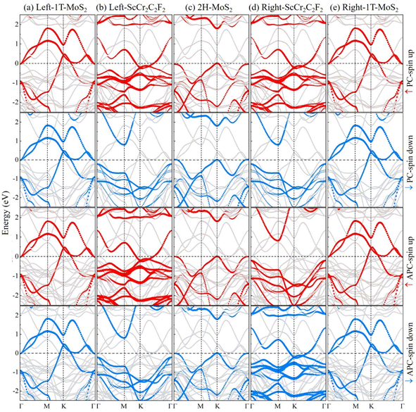
To investigate whether the half-metallicity of ScCr2C2F2 can be retained in vdW MTJs, we calculated the spin-dependent projected band structures of the 1T-MoS2/ScCr2C2F2/2H-MoS2/ScCr2C2F2/1T-MoS2 heterostructure when the ScCr2C2F2 layers are in PC and APC states. Compared with the band structures of corresponding monolayers in Fig. 2, the projected band structures of the 1T-MoS2 and 2H-MoS2 layers move up with respect to the Fermi level, as shown in Fig. 5a, c and e. On the other hand, a conversely downward shift is found for the projected band structures of the ScCr2C2F2 layers, as shown in Fig. 5b and d. The energy-level shift agrees well with the charge transfers of electrons in the process of forming the heterostructure we have shown previously. Furthermore, the half-metallic electronic structures of the left and right ScCr2C2F2 layers are well maintained, and only the spin-up channel of the PC state is conductive, while the other three channels are insulating. The difference in transmission mainly comes from the spin-up channel of ScCr2C2F2 that allows the electrons to pass through, while its spin-down channel prevents electrons from passing through. Therefore, the spin filter effect is mainly contributed by the spin-resolved band structures of ScCr2C2F2, rather than the interface between ScCr2C2F2 and 2H-MoS2. Tis phenomenon reveals a large conductivity difference between PC and APC states, which indicates a distinguished performance of the ScCr2C2F2-based vdW MTJs.
 |
| | Fig. 5 The spin-dependent projected band structures of (a) left-1T-MoS2 (b) left-ScCr2C2F2 (c) 2H-MoS2 (d) right-ScCr2C2F2 and (e) right-1T-MoS2 in the 1T-MoS2/ScCr2C2F2/2H-MoS2/ScCr2C2F2/1T-MoS2 heterostructure. | |
Furthermore, to understand the thickness effects of the tunnel barrier, odd layer number 2H-MoS2 with different layer n (n = 1, 3, 5) was taken into account, following the principle of control variables. In the following discussion, 1T-MoS2/ScCr2C2F2/2H-MoS2/ScCr2C2F2/1T-MoS2 vdW MTJs with one, three and five 2H-MoS2 layers are abbreviated as MTJ-HM, MTJ-3HM and MTJ-5HM, respectively. The corresponding atomically structured schematics of the vdW MTJs are illustrated in Fig. 6. Herein, after the full-structure optimizations of the vdW MTJs, the relaxed interface distances between different materials are summarized in Table 2. For all the vdW MTJs, the distances between 2H-MoS2 and ScCr2C2F2 (dLC and dRC) are around 2.7–3 Å, and the distances between 1T-MoS2 and ScCr2C2F2 (dL and dR) hold smaller values around 2.4–2.5 Å, revealing weak vdW connections in the MTJs.
 |
| | Fig. 6 The schematic illustrations of 1T-MoS2/ScCr2C2F2/2H-MoS2/ScCr2C2F2/1T-MoS2 vdW MTJs with (a) one (MTJ-HM) (b) three (MTJ-3HM) and (c) five (MTJ-5HM) 2H-MoS2 tunnel barrier layers. | |
Table 2 The interface distances dL, dLC, dRC and dR (Å) of left-1T-MoS2/left-ScCr2C2F2, left-ScCr2C2F2/2H-MoS2, 2H-MoS2/right-ScCr2C2F2 and right-ScCr2C2F2/right-1T-MoS2 interfaces in different vdW MTJs
| MTJs |
d
L
|
d
LC
|
d
RC
|
d
R
|
| MTJ-HM |
2.44 |
3.01 |
2.93 |
2.49 |
| MTJ-3HM |
2.48 |
2.76 |
2.76 |
2.48 |
| MTJ-5HM |
2.48 |
2.72 |
2.78 |
2.44 |
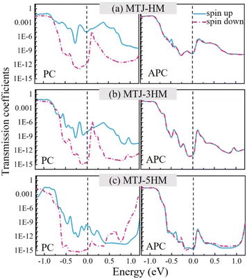
To investigate the spin-dependent transport properties, we calculated the transmission coefficients at the equilibrium state for the 1T-MoS2/ScCr2C2F2/2H-MoS2/ScCr2C2F2/1T-MoS2 vdW MTJs. Fig. 7 shows the zero-bias transmission coefficient curves from −1.2 eV to 1.2 eV for MTJ-HM, MTJ-3HM, and MTJ-5HM in PC and APC states. For all the vdW MTJs in the PC state, the maximum spin-up and spin-down transmission coefficients appear around −1 eV below the Fermi level, and the spin-down transmission coefficients suffer more reduction than spin-up transmission coefficients with the energy region approaching the Fermi level. Therefore, the spin-up transmission coefficients at the Fermi level are several orders of magnitude larger than the spin-down transmission coefficients. Herein, the spin-up channel plays a decisive role in the transmission process. When the vdW MTJs are in an APC state, the spin-up transmission coefficients are almost equivalent to the spin-down transmission coefficients of the entire energy region, and the minimum values occur around the Fermi level. Hence, the transmission capacity of both spin channels is tiny in the APC state.
 |
| | Fig. 7 The transmission coefficients for (a) MTJ-HM, (b) MTJ-3HM, and (c) MTJ-5HM in PC and APC states. | |
To quantitatively analyse the device performance of the 1T-MoS2/ScCr2C2F2/2H-MoS2/ScCr2C2F2/1T-MoS2 vdW MTJs, the TMR ratios can be calculated using the following equation14,72
| | | TMR = (GPC − GAPC)/GAPC × 100% | (4) |
where
GPC and
GAPC are the total spin-dependent conductance of the PC and APC states, which are defined as
| | | GPC = T↑PC(Ef) + T↓PC(Ef) | (5) |
| | | GAPC = T↑APC(Ef) + T↓APC(Ef) | (6) |
where
T↑PC(
Ef) and
T↓PC(
Ef) represent the spin-up and spin-down transmission coefficients at the Fermi level when the vdW MTJs are in the PC state, and
T↑APC(
Ef) and
T↓APC(
Ef) represent the spin-up and spin-down transmission coefficients, respectively, at the Fermi level when the vdW MTJs are in the APC state.
Table 3 lists the calculated spin-dependent transmission coefficients at the Fermi level, total spin-dependent conductances, and TMR ratios. It was observed that the total spin-dependent conductances decrease exponentially with the increase in the 2H-MoS
2 barrier layers. It was noted that
GPC of MTJ-HM is five orders of magnitude larger than
GAPC, which results in the giant TMR ratios of 2.95 × 10
6%. Interestingly, although,
GPC and
GAPC was reduced by several orders of magnitude, when the tunnel-barrier 2H-MoS
2 increases to three layers, the TMR ratio of MTJ-3HM increases to 6.95 × 10
6% since the corresponding
GPC is six orders of magnitude larger than
GAPC. Besides, when the number of tunnel-barrier 2H-MoS
2 increases to five layers, the TMR ratios of MTJ-5HM decrease to 9.24 × 10
5%, which is still a considerable giant value. Furthermore, the transmission calculations by including the spin–orbit coupling (SOC) are shown in Table S1.
† It is noted that the SOC should contribute to the spin-flip scattering, enhancing the transmission probability in antiparallel configuration and reducing the TMR. Nevertheless, the proposed vdW MTJ devices showed considerable TMR values at a 10
4% level.
Table 3 The calculated transmission coefficients (e2/h) of the spin-up channel in the PC state T↑PC(Ef), spin-down channel in the PC state T↓PC(Ef), spin-up channel in the APC state T↑APC(Ef), and spin-down channel in the APC state T↓APC(Ef), total spin-dependent conductances (e2/h) in the PC state GPC and the APC state GAPC, and TMR ratios for MTJ-HM, MTJ-3HM, and MTJ-5HM devices
| MTJs |
T
PC
↑(Ef) |
T
PC
↓(Ef) |
T
APC
↑(Ef) |
T
APC
↓(Ef) |
G
PC
|
G
APC
|
TMR (%) |
| MTJ-HM |
1.19 × 10⁻⁵ |
1.76 × 10⁻¹² |
2.03 × 10⁻¹⁰ |
2.02 × 10⁻¹⁰ |
1.19 × 10⁻⁵ |
4.05 × 10⁻¹⁰ |
2.95 × 10⁶ |
| MTJ-3HM |
1.30 × 10⁻⁸ |
3.43 × 10⁻¹⁵ |
9.36 × 10⁻¹⁴ |
9.27 × 10⁻¹⁴ |
1.30 × 10⁻⁸ |
1.86 × 10⁻¹³ |
6.95 × 10⁶ |
| MTJ-5HM |
5.51 × 10⁻¹¹ |
1.96 × 10⁻¹⁵ |
2.32 × 10⁻¹⁵ |
3.64 × 10⁻¹⁵ |
5.51 × 10⁻¹¹ |
5.96 × 10⁻¹⁵ |
9.24 × 10⁵ |
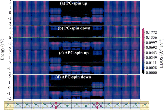
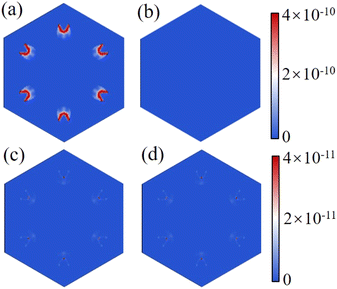
Moreover, we calculated the spin-dependent k‖-resolved transmission spectrums at the Fermi level to better represent the physical origin of the giant TMR effects in the 1T-MoS2/ScCr2C2F2/2H-MoS2/ScCr2C2F2/1T-MoS2 vdW MTJs. Herein, Fig. 8 illustrates the transmission spectrum of MTJ-3HM as an example since it shows the highest TMR ratio. For reference, the transmission spectra of MTJ-HM and MTJ-5HM are presented in Fig. S3 and S4,† respectively. Fig. 8a shows that there are six crescent-shaped high transmission regions in the spin-up transmission spectrum for MTJ-3HM in the PC state. However, there is no distinguishable high transmission region in the whole k‖-resolved regions for the spin-down transmission spectrum in Fig. 8b. On the other hand, the transmission regions of both spin-up and spin-down channels are similar for MTJ-3HM in the APC state. Herein, it is noted that the transmission capacity of the APC state is several orders of magnitude smaller than that of the PC state, which leads to the apparent TMR effect. In addition, the spin-dependent projected local density of states of MTJ-HM, MTJ-3HM, and MTJ-5HM along the transport direction are shown in Fig. S5, 9 and S6,† respectively. The corresponding vdW MTJ model is illustrated in the bottom panel for reference. Regardless of the PC or APC states, it was observed that the 1T-MoS2 electrodes and 2H-MoS2 barriers still exhibit their metallic and semiconducting properties, respectively. However, the ScCr2C2F2 monolayer shows metallic properties in the spin-up channel but presents a semiconducting feature in the spin-down channel in the PC state and vice versa in the APC state. As a result, in the PC state, for the electron transport process from the left to right in the 1T-MoS2 electrodes, the spin-up electrons only need to go through the potential barrier of the 2H-MoS2 layer. However, the spin-down electrons have to overcome a much higher potential barrier, which is from the left and right ScCr2C2F2 layers as well as the 2H-MoS2 layers. On the other hand, in the APC state, the spin-up (spin-down) electrons have to overcome the potential barriers of the right (left) ScCr2C2F2 layer and the 2H-MoS2 layers for the electron transport process from the left to right 1T-MoS2 electrodes. Therefore, the spin-up electrons in the PC state are proved to play a decisive role in the transmission behavior, which agrees well with our previously electronic structure analysis.
 |
| | Fig. 8 The spin-dependent k‖-resolved transmission spectrums of MTJ-3HM at the Fermi level for (a) spin-up and (b) spin-down channels in the PC state and (c) spin-up and (d) spin-down channels in the APC state. | |
 |
| | Fig. 9 The spin-dependent projected local density of states of MTJ-3HM for (a) spin-up and (b) spin-down channels in the PC state, (c) spin-up, and (d) spin-down channels in the APC state. | |
Conclusion
In summary, by combining density functional theory and nonequilibrium Green's function calculations, we investigated the transport properties of 1T-MoS2/ScCr2C2F2/2H-MoS2/ScCr2C2F2/1T-MoS2 vdW MTJs with different thicknesses of the 2H-MoS2 tunnel barrier. The different stacking configurations of ScCr2C2F2 relative to 1T-MoS2 and 2H-MoS2 were firstly studied to determine the stable interface configurations. The calculated formation energies and binding energies indicated that all the interface configurations can form spontaneously. Besides, the interlayer charge transfers from the 1T-MoS2/2H-MoS2 to ScCr2C2F2 layers can be inferred due to the work function differences. The projected band structures of the corresponding 1T-MoS2/ScCr2C2F2/2H-MoS2/ScCr2C2F2/1T-MoS2 heterostructure revealed that the ScCr2C2F2 monolayer can still maintain half-metallicity with perfect polarization in vdW MTJs. Subsequently, the thickness of the 2H-MoS2 tunnel barrier was considered for further performance optimizations. It is remarkable to note that all the vdW MTJs hold giant TMR ratios over 9 × 10⁵%, and the maximum TMR ratio of 6.95 × 10⁶% was obtained in vdW MTJ with a trilayer 2H-MoS2 tunnel barrier, demonstrating the potential of such vdW MTJs for applications.
Conflicts of interest
The authors declare no competing financial interest.
Acknowledgements
This work was supported by the National Natural Science Foundation of China (Grant No. 52201022, 21973012, 51872017, and 51871009), the Natural Science Foundation of Fujian Province (Grant No. 2021J06011, 2020J01351, 2020J01474, and 2021J01590), and the “Qishan Scholar” Scientific Research Project of Fuzhou University.
References
- J. G. Zhu and C. Park, Mater. Today, 2006, 9, 36–45 CrossRef CAS.
- A. Hirohata, K. Yamada, Y. Nakatani, I. L. Prejbeanu, B. Diény, P. Pirro and B. Hillebrands, J. Magn. Magn. Mater., 2020, 509, 166711 CrossRef CAS.
- A. D. Kent and D. C. Worledge, Nat. Nanotechnol., 2015, 10, 187–191 CrossRef CAS PubMed.
- J. M. Hu, Z. Li, L. Q. Chen and C. W. Nan, Nat. Commun., 2011, 2, 553 CrossRef PubMed.
- S. Bhatti, R. Sbiaa, A. Hirohata, H. Ohno, S. Fukami and S. N. Piramanayagam, Mater. Today, 2017, 20, 530–548 CrossRef.
- A. Hirohata and K. Takanashi, J. Phys. D: Appl. Phys., 2014, 47, 193001 CrossRef.
- M. Julliere, Phys. Lett., 1975, 54A, 225–226 CrossRef CAS.
- H. Lu, Y. Guo and J. Robertson, ACS Appl. Mater. Interfaces, 2021, 13, 47226–47235 CrossRef CAS.
- Y. Feng, H. Ding, X. Li, B. Wu and H. Chen, J. Appl. Phys., 2022, 131, 133901 CrossRef CAS.
- Y. Guo, Y. Zhang, S. Yuan, B. Wang and J. Wang, Nanoscale, 2018, 10, 18036–18042 RSC.
- Y. Shen, D. Kan, I. C. Lin, M. W. Chu, I. Suzuki and Y. Shimakawa, Appl. Phys. Lett., 2020, 117, 042408 CrossRef CAS.
- P. M. Tedrow and R. Meservey, Phys. Rev. B: Solid State, 1973, 7, 318–326 CrossRef CAS.
- T. Miyazaki and N. Tezuka, J. Magn. Magn. Mater., 1995, 139, L231–L234 CrossRef CAS.
- S. Yuasa, T. Nagahama, A. Fukushima, Y. Suzuki and K. Ando, Nat. Mater., 2004, 3, 868–871 CrossRef CAS.
- J. S. Moodera, L. R. Kinder, T. M. Wong and R. Meservey, Phys. Rev. Lett., 1995, 74, 3273–3276 CrossRef CAS PubMed.
- T. Ishikawa, T. Marukame, H. Kijima, K. I. Matsuda, T. Uemura, M. Arita and M. Yamamoto, Appl. Phys. Lett., 2006, 89, 192505 CrossRef.
- W. H. Wang, H. Sukegawa, R. Shan, S. Mitani and K. Inomata, Appl. Phys. Lett., 2009, 95, 182502 CrossRef.
- B. Yang, L. Tao, L. Jiang, W. Chen, P. Tang, Y. Yan and X. Han, Phys. Rev. Appl., 2018, 9, 054019 CrossRef.
- R. A. de Groot, F. M. Mueller, P. G. van Engen and K. H. J. Buschow, Phys. Rev. Lett., 1983, 50, 2024–2027 CrossRef CAS.
- T. Scheike, H. Sukegawa, T. Furubayashi, Z. Wen, K. Inomata, T. Ohkubo, K. Hono and S. Mitani, Appl. Phys. Lett., 2014, 105, 242407 CrossRef.
- S. Cardoso, P. P. Freitas, C. de Jesus, P. Wei and J. C. Soares, Appl. Phys. Lett., 2000, 76, 610–612 CrossRef CAS.
- B. Huang, G. Clark, E. Navarro-Moratalla, D. R. Klein, R. Cheng, K. L. Seyler, D. Zhong, E. Schmidgall, M. A. McGuire, D. H. Cobden, W. Yao, D. Xiao, P. Jarillo-Herrero and X. Xu, Nature, 2017, 546, 270–273 CrossRef CAS PubMed.
- C. Gong, L. Li, Z. Li, H. Ji, A. Stern, Y. Xia, T. Cao, W. Bao, C. Wang, Y. Wang, Z. Q. Qiu, R. J. Cava, S. G. Louie, J. Xia and X. Zhang, Nature, 2017, 546, 265–269 CrossRef CAS PubMed.
- Y. Deng, Y. Yu, Y. Song, J. Zhang, N. Z. Wang, Z. Sun, Y. Yi, Y. Z. Wu, S. Wu, J. Zhu, J. Wang, X. H. Chen and Y. Zhang, Nature, 2018, 563, 94–99 CrossRef CAS PubMed.
- Q. Liu, Y. Wang, Y. Zhao, Y. Guo, X. Jiang and J. Zhao, Adv. Funct. Mater., 2022, 2113126 CrossRef CAS.
- Z. Wang, D. Sapkota, T. Taniguchi, K. Watanabe, D. Mandrus and A. F. Morpurgo, Nano Lett., 2018, 18, 4303–4308 CrossRef CAS PubMed.
- T. Song, M. W. Tu, X. Zhang, B. Huang, N. P. Wilson, K. L. Seyler, L. Zhu, T. Taniguchi, K. Watanabe, M. A. McGuire, D. H. Cobden, D. Xiao, W. Yao and X. Xu, Science, 2018, 360, 1214–1218 CrossRef CAS PubMed.
- X. Zhang, Y. Guo, Z. Zhou, X. Zhang, Y. Chen, X. C. Zeng and J. Wang, Adv. Funct. Mater., 2022, 2200154 CrossRef CAS.
- W. Yang, Y. Cao, J. Han, X. Lin, X. Wang, G. Wei, C. Lv, A. Bournel and W. Zhao, Nanoscale, 2021, 13, 862–868 RSC.
- J. Li, M. Di, Z. Yang, L. C. Xu, Y. Yang and X. Liu, Phys. Chem. Chem. Phys., 2019, 21, 2734–2742 RSC.
- L. L. Tao and J. Wang, Nanoscale, 2017, 9, 12684–12689 RSC.
- K. Huang, Z. Li, J. Lin, G. Han and P. Huang, Chem. Soc. Rev., 2018, 47, 5109–5124 RSC.
- K. R. G. Lim, A. D. Handoko, S. K. Nemani, B. Wyatt, H. Y. Jiang, J. Tang, B. Anasori and Z. W. Seh, ACS Nano, 2020, 14, 10834–10864 CrossRef CAS PubMed.
- F. Shahzad, A. Iqbal, H. Kim and C. M. Koo, Adv. Mater., 2020, 32, 2002159 CrossRef CAS PubMed.
- M. Alhabeb, K. Maleski, B. Anasori, P. Lelyukh, L. Clark, S. Sin and Y. Gogotsi, Chem. Mater., 2017, 29, 7633–7644 CrossRef CAS.
- C. Si, J. Zhou and Z. Sun, ACS Appl. Mater. Interfaces, 2015, 7, 17510–17515 CrossRef CAS PubMed.
- Q. Sun, J. Li, Y. Li, Z. Yang and R. Wu, Appl. Phys. Lett., 2021, 119, 062404 CrossRef CAS.
- J. He, P. Lyu and P. Nachtigall, J. Mater. Chem. C, 2016, 4, 11143–11149 RSC.
- E. Balci, U. O. Akkus and S. Berber, ACS Appl. Mater. Interfaces, 2019, 11, 3609–3616 CrossRef CAS PubMed.
- J. Yang, S. Zhang, L. Li, A. Wang, Z. Zhong and L. Chen, Matter, 2019, 1, 1304–1315 CrossRef.
- B. Anasori, Y. Xie, M. Beidaghi, J. Lu, B. C. Hosler, L. Hultman, P. R. C. Kent, Y. Gogotsi and M. W. Barsoum, ACS Nano, 2015, 9, 9507–9516 CrossRef CAS.
- W. Hong, B. C. Wyatt, S. K. Nemani and B. Anasori, MRS Bull., 2020, 45, 850–861 CrossRef.
- Y. W. Cheng, J. H. Dai, Y. M. Zhang and Y. Song, J. Phys. Chem. C, 2018, 122, 28113–28122 CrossRef CAS.
- L. Dong, H. Kumar, B. Anasori, Y. Gogotsi and V. B. Shenoy, J. Phys. Chem. Lett., 2017, 8, 422–428 CrossRef CAS PubMed.
- Z. Jing, H. Wang, X. Feng, B. Xiao, Y. Ding, K. Wu and Y. Cheng, J. Phys. Chem. Lett., 2019, 10, 5721–5728 CrossRef CAS PubMed.
- Y. Zhang, Z. Cui, B. Sa, N. Miao, J. Zhou and Z. Sun, Nanoscale Horiz., 2022, 7, 276–287 RSC.
- Z. Shen, X. Bo, K. Cao, X. Wan and L. He, Phys. Rev. B, 2021, 103, 085102 CrossRef CAS.
- G. Wang, L. Peng, K. Li, L. Zhu, J. Zhou, N. Miao and Z. Sun, Comput. Mater. Sci., 2021, 186, 110064 CrossRef CAS.
- G. Wang, K. Li, L. Peng, Y. Zhang, J. Zhou and Z. Sun, Acta Metall. Sin., 2022, 58, 75–88 Search PubMed.
- G. Kresse and J. Furthmüller, Phys. Rev. B: Condens. Matter Mater. Phys., 1996, 54, 11169 CrossRef CAS PubMed.
- J. P. Perdew, K. Burke and M. Ernzerhof, Phys. Rev. Lett., 1996, 77, 3865 CrossRef CAS PubMed.
- H. Kumar, N. C. Frey, L. Dong, B. Anasori, Y. Gogotsi and V. B. Shenoy, ACS Nano, 2017, 11, 7648–7655 CrossRef CAS PubMed.
- S. Grimme, J. Antony, S. Ehrlich and H. Krieg, J. Chem. Phys., 2010, 132, 154104 CrossRef PubMed.
- S. Grimme, S. Ehrlich and L. Goerigk, J. Comput. Chem., 2011, 32, 1456–1465 CrossRef CAS PubMed.
- S. Smidstrup, T. Markussen, P. Vancraeyveld, J. Wellendorff, J. Schneider, T. Gunst, B. Verstichel, D. Stradi, P. A. Khomyakov, U. G. Vej-Hansen, M. E. Lee, S. T. Chill, F. Rasmussen, G. Penazzi, F. Corsetti, A. Ojanpera, K. Jensen, M. L. N. Palsgaard, U. Martinez, A. Blom, M. Brandbyge and K. Stokbro, J. Phys.: Condens. Matter, 2020, 32, 015901 CrossRef CAS.
- M. Brandbyge, J. L. Mozos, P. Ordejón, J. Taylor and K. Stokbro, Phys. Rev. B: Condens. Matter Mater. Phys., 2002, 65, 165401 CrossRef.
- M. J. van Setten, M. Giantomassi, E. Bousquet, M. J. Verstraete, D. R. Hamann, X. Gonze and G. M. Rignanese, Comput. Phys. Commun., 2018, 226, 39–54 CrossRef CAS.
- V. Blum, R. Gehrke, F. Hanke, P. Havu, V. Havu, X. Ren, K. Reuter and M. Scheffler, Comput. Phys. Commun., 2009, 180, 2175–2196 CrossRef CAS.
- Y. Guo, X. Yu, Y. Zhang, X. Zhang, S. Yuan, Y. Li, S. A. Yang and J. Wang, ACS Nano, 2022, 16, 11174–11181 CrossRef CAS PubMed.
- M. Julliere, Phys. Lett., 1975, 54A, 225–227 CrossRef CAS.
- Z. Diao, Z. Li, S. Wang, Y. Ding, A. Panchula, E. Chen, L. C. Wang and Y. Huai, J. Phys.: Condens. Matter, 2007, 19, 165209 CrossRef.
- J. Z. Sun and D. C. Ralph, J. Magn. Magn. Mater., 2008, 320, 1227–1237 CrossRef CAS.
- M. Kan, J. Y. Wang, X. W. Li, S. H. Zhang, Y. W. Li, Y. Kawazoe, Q. Sun and P. Jena, J. Phys. Chem. C, 2014, 118, 1515–1522 CrossRef CAS.
- R. Kappera, D. Voiry, S. E. Yalcin, B. Branch, G. Gupta, A. D. Mohite and M. Chhowalla, Nat. Mater., 2014, 13, 1128–1134 CrossRef CAS PubMed.
- F. Raffone, C. Ataca, J. C. Grossman and G. Cicero, J. Phys. Chem. Lett., 2016, 7, 2304–2309 CrossRef CAS PubMed.
- J. N. Coleman, M. Lotya, A. O'Neill, S. D. Bergin, P. J. King, U. Khan, K. Young, A. Gaucher, S. De, R. J. Smith, I. V. Shvets, S. K. Arora, G. Stanton, H. Y. Kim, K. Lee, G. T. Kim, G. S. Duesberg, T. Hallam, J. J. Boland, J. J. Wang, J. F. Donegan, J. C. Grunlan, G. Moriarty, A. Shmeliov, R. J. Nicholls, J. M. Perkins, E. M. Grieveson, K. Theuwissen, D. W. McComb, P. D. Nellist and V. Nicolosi, Science, 2011, 331, 568 CrossRef CAS PubMed.
- J. Liao, B. Sa, J. Zhou, R. Ahuja and Z. Sun, J. Phys. Chem. C, 2014, 118, 17594–17599 CrossRef CAS.
- L. F. Wang, T. B. Ma, Y. Z. Hu, Q. Zheng, H. Wang and J. Luo, Nanotechnology, 2014, 25, 385701 CrossRef PubMed.
- S. Gbadamasi, M. Mohiuddin, V. Krishnamurthi, R. Verma, M. W. Khan, S. Pathak, K. Kalantar-Zadeh and N. Mahmood, Chem. Soc. Rev., 2021, 50, 4684–4729 RSC.
- X. Hu, X. Li, G. Li, T. Ji, F. Ai, J. Wu, E. Ha and J. Hu, Adv. Funct. Mater., 2021, 31, 2011284 CrossRef CAS.
- J. Kang, W. Liu, D. Sarkar, D. Jena and K. Banerjee, Phys. Rev. X, 2014, 4, 031005 CAS.
- S. S. Parkin, C. Kaiser, A. Panchula, P. M. Rice, B. Hughes, M. Samant and S. H. Yang, Nat. Mater., 2004, 3, 862–867 CrossRef CAS PubMed.
|
| This journal is © The Royal Society of Chemistry 2022 |
Click here to see how this site uses Cookies. View our privacy policy here.  Open Access Article
 a,
Jian
Zhou
 c,
Baisheng
Sa
 *a and
Zhimei
Sun
 *c
*c
![[thin space (1/6-em)]](https://www.rsc.org/images/entities/char_2009.gif) 000% has been experimentally realized by increasing the CrI3 layer thickness.27 It is theoretically predicted that a giant zero-bias TMR ratio of up to 48
000% has been experimentally realized by increasing the CrI3 layer thickness.27 It is theoretically predicted that a giant zero-bias TMR ratio of up to 48![[thin space (1/6-em)]](https://www.rsc.org/images/entities/char_2009.gif) 000% can be achieved using CrOCl/CrOX bilayer as the spin-filter tunnel barriers.28 On the other hand, the vdW MTJs based on 1T-VSe2 possess a high TMR ratio of 5600%, and the TMR ratio is sharply increased to 1.7 × 10⁵% by inserting 2H-MoSe2.29 Two kinds of 6,6,12-graphyne-based molecular magnetic tunnel junctions have novel transport behaviors, and the maximum order of magnitude of tunneling magnetoresistance values reaches 106%.30 Wang et al. reported the spin-dependent transport properties of a molecular junction made of two manganese phthalocyanine molecules linked by single-walled carbon nanotubes and predicted a high spin-filter efficiency and magnetoresistance ratio.31 However, it is still challenging to develop 2D materials with intrinsic magnetism to achieve giant TMR ratios in MTJs.
000% can be achieved using CrOCl/CrOX bilayer as the spin-filter tunnel barriers.28 On the other hand, the vdW MTJs based on 1T-VSe2 possess a high TMR ratio of 5600%, and the TMR ratio is sharply increased to 1.7 × 10⁵% by inserting 2H-MoSe2.29 Two kinds of 6,6,12-graphyne-based molecular magnetic tunnel junctions have novel transport behaviors, and the maximum order of magnitude of tunneling magnetoresistance values reaches 106%.30 Wang et al. reported the spin-dependent transport properties of a molecular junction made of two manganese phthalocyanine molecules linked by single-walled carbon nanotubes and predicted a high spin-filter efficiency and magnetoresistance ratio.31 However, it is still challenging to develop 2D materials with intrinsic magnetism to achieve giant TMR ratios in MTJs. 41,42 offer more possibilities for fantastic magnetic properties.43–45 Recently, impressive intrinsic magnetic properties have been found in HM DTM MXenes, such as ScCr2C2F2, ZrCr2C2H2 and YCr2C2H2.46 Herein, ScCr2C2F2 presents a high Curie temperature of 230 K based on the Metropolis Monte Carlo (MC) simulations. Although TC could be theoretically overestimated, recently good agreement between theoretical results and experimental values have been achieved, for instance, in the case of CrI3 and Fe3GeTe2.46,47 The MC predicted TC of 230 K indicates that ScCr2C2F2 is anticipated to achieve distinguished MTJ performance as the ferromagnetic electrodes. Therefore, a systematical understanding and optimization of ScCr2C2F2-based vdW MTJs are of great interest and importance.

![[3 with combining macron]](https://www.rsc.org/images/entities/char_0033_0304.gif) m1, and 2H-MoS2 has the space group of P
m1, and 2H-MoS2 has the space group of P![[6 with combining macron]](https://www.rsc.org/images/entities/char_0036_0304.gif) m2. The optimized lattice constant of ScCr2C2F2 is 3.12 Å. The optimized lattice constants of both 1T-MoS2 and 2H-MoS2 are 3.18 Å, which not only agrees well with the experimental values,63–66 but also exhibits a perfect lattice match with ScCr2C2F2. Fig. 2d and f illustrates the calculated band structures for ScCr2C2F2, 1T-MoS2, and 2H-MoS2 monolayers. From Fig. 2d, ScCr2C2F2 shows the metallic properties in the spin-up channel and semiconducting properties in the spin-down channel, revealing its half-metallic magnetic features. On the other hand, from Fig. 2e and f, 1T-MoS2 and 2H-MoS2 are demonstrated to be metallic conducting and semiconducting, respectively. Therefore, 1T-MoS2 and 2H-MoS2 could be employed as the electrodes and tunnel barrier for the vdW MTJs.
m2. The optimized lattice constant of ScCr2C2F2 is 3.12 Å. The optimized lattice constants of both 1T-MoS2 and 2H-MoS2 are 3.18 Å, which not only agrees well with the experimental values,63–66 but also exhibits a perfect lattice match with ScCr2C2F2. Fig. 2d and f illustrates the calculated band structures for ScCr2C2F2, 1T-MoS2, and 2H-MoS2 monolayers. From Fig. 2d, ScCr2C2F2 shows the metallic properties in the spin-up channel and semiconducting properties in the spin-down channel, revealing its half-metallic magnetic features. On the other hand, from Fig. 2e and f, 1T-MoS2 and 2H-MoS2 are demonstrated to be metallic conducting and semiconducting, respectively. Therefore, 1T-MoS2 and 2H-MoS2 could be employed as the electrodes and tunnel barrier for the vdW MTJs.


 stand for the total energies of ScCr2C2F2 and 1T-MoS2 (or 2H-MoS2) monolayers constrained in the corresponding heterostructure lattice, respectively. S is the interface area. EScCr2C2F2 and EMoS2 represent the free-standing total energies of ScCr2C2F2 and 1T-MoS2 (or 2H-MoS2) monolayers. The calculated Ebind and Eform are summarized in Table 1. The negative Ebind and Eform demonstrate that all the stacking configurations of ScCr2C2F2/1T-MoS2 and ScCr2C2F2/2H-MoS2 heterostructures can form spontaneously. It is worth noting that the stacking-II of ScCr2C2F2/1T-MoS2 heterostructure and stacking-I of ScCr2C2F2/1T-MoS2 heterostructure are more favorable to exist in experiments due to their lowest Ebind and Eform among various stacking configurations in Table 1. Based on the Ebind and Eform results, energetically-favorable stacking-II for the ScCr2C2F2/1T-MoS2 interface and stacking-I configurations for the ScCr2C2F2/1T-MoS2 interface were selected to construct the vdW MTJs.
