 Open Access Article
Low-temperature solution-processed SnO2 electron transport layer modified by oxygen plasma for planar perovskite solar cells†
Akshaiya Padmalatha Muthukrishnana,
Junyeoung Leea,
Jongbok Kim b,
Chang Su Kimc and
Sungjin Jo
 *a
*a
aSchool of Energy Engineering, Kyungpook National University, Daegu 41566, Republic of Korea. E-mail: sungjin@knu.ac.kr
bDepartment of Materials Science and Engineering, Kumoh National Institute of Technology, Gumi 39177, Republic of Korea
cDepartment of Advanced Functional Thin Films, Surface Technology Division, Korea Institute of Materials Science, 797 Changwondaero, Sungsan-Gu, Changwon, Gyeongnam 51508, Republic of Korea
First published on 9th February 2022
Abstract
SnO2 has attracted significant attention as an electron transport layer (ETL) because of its wide optical bandgap, electron mobility, and transparency. However, the annealing temperature of 180 °C–200 °C, as reported by several studies, for the fabrication of SnO2 ETL limits its application for flexible devices. Herein, we demonstrated that the low-temperature deposition of SnO2 ETL and further surface modification with oxygen plasma enhances its efficiency from 2.3% to 15.30%. Oxygen plasma treatment improves the wettability of the low-temperature processed SnO2 ETL that results in a larger perovskite grain size. Hence, oxygen plasma treatment effectively improves the efficiency of perovskite solar cells at a low temperature and is compatible with flexible applications.
1. Introduction
Among the next-generation solar cells, organic–inorganic hybrid perovskite solar cells (PSCs) have emerged as a nascent technology in recent years due to their high photoelectric power-conversion efficiency (PCE), low cost, and ease of fabrication. Intensive research on light-absorbing materials, electron transport layers (ETLs), and hole transport layers (HTLs) resulted in a drastic improvement in the PCE from 3.8% to 25.5% over the past decade.1–6 Generally, n-i-p planar structures are employed in most state-of-the-art PSCs where the perovskite light-absorbing layer is sandwiched between the ETL and HTL.7 Appropriate selection of the ETL plays a dominant role in determining the performance of PSCs by effectively extracting and transporting photogenerated electrons from the perovskite layer to the electrodes. Recently, extensive research has been focused on metal oxide-based ETLs, such as TiO2, SnO2, ZnO, InO3, and Nb2O5, for planar structure-based PSCs.8–13Although most of the highly efficient PSCs employ TiO2 as the ETL, the high-temperature sintering process, low mobility, and instability under ultraviolet (UV) light limit its application for flexible and commercial PSCs. In contrast, SnO2 has attracted attention as an excellent alternative to TiO2 because of its distinct advantages, such as its wide optical bandgap, high electron mobility, and good optical stability. It can be also processed at lower temperatures than TiO2,14–17 and several studies have reported the fabrication of SnO2 ETL at annealing temperatures of 180 °C–200 °C.18–21 However, the required fabrication temperature is still high and incompatible with most plastic substrates. To circumvent this problem, alternative annealing methods have been developed, such as UV, vacuum, and microwave-assisted annealing, to facilitate the formation of the metal oxide layer at low temperatures. For example, Xiaodong Ren et al. used a UV ozone illumination to prepare a chlorinated SnO2 as ETL for PSC.22,23 Huang et al. employed UV-assisted annealing of SnO2 film as a low-temperature ETL for PSCs.24 In addition, Menghua et al. effectively prepared SnO2 ETL via an in-pulsed photonic annealing technique.25 These low-temperature methodologies lead to the formation of SnO2 ETLs at a low temperature, but the device characteristics in these studies were lower than those obtained using thermally annealed SnO2. Therefore, there is a desperate need for an innovative precursor-to-metal oxide conversion strategy capable of breaking the alkoxy and hydroxyl groups to form a metal–oxide–metal network, thereby producing a high-quality SnO2 ETL at a low temperature.
In this study, we adopt a simple and effective oxygen plasma treatment on low-temperature deposited SnO2 (LT-SnO2) ETL. In this method, a sol–gel-coated SnO2 layer is activated by the highly reactive and energetic species in the plasma, which facilitates a rapid precursor-to-metal oxide conversion at a low temperature. The low-temperature SnO2 modified by oxygen plasma (LTP-SnO2) retains material properties comparable to those of high-temperature annealed SnO2 (HT-SnO2). Therefore, the LTP-SnO2 ETL-based PSCs show a significant improvement over LT-SnO2 ETL-based PSCs. Moreover, surface modification with oxygen plasma improves the wettability of LT-SnO2, which in turn increases the grain size of CH3NH3PbI3 (MAPbI3), resulting in reduced charge recombination at the grain boundaries. After undergoing plasma treatment, the PCE of PSC based on LT-SnO2 and LTP-SnO2 increases from 2.3% to 15.30%. Further, the open-circuit voltage (Voc) of LT-SnO2 based PSC increases rapidly from 0.34 to 1.06 V after plasma treatment, which indicates the suppression of charge recombination at the ETL/MAPbI3 interface. This study demonstrates the efficacy of low-temperature fabrication of PSCs for future applications.
2. Materials and methods
2.1 Synthesis of SnO2
Facile synthesis of SnO2 sol–gel was carried out using the solution-processed method. SnCl2·2H2O was dissolved in ethanol to obtain a precursor solution with a concentration of 0.05 M. The solution was stirred at 1000 rpm for 24 h. Before the solution is spin-coated on a fluorine-doped tin oxide (FTO) substrate, it is filtered with a polytetrafluoroethylene filter to obtain a clear and homogeneous solution without any impurities. The reaction mechanism involved in the formation of SnO2 during the synthesis process is given below.26| SnCl2·2H2O + C2H5OH → Sn(OH)2 + C2H5Cl |
| Sn(OH)2 → SnO + H2O |
| SnO → SnO2 |
2.2 Fabrication of SnO2 layer and perovskite solar cell
SnO2 film is prepared by spin coating the above precursor solution on an FTO substrate at 2000 rpm for 30 s and then heated at a temperature of 200 °C and 150 °C for high-temperature and low-temperature annealing, respectively. Oxygen plasma treatment was performed on low-temperature annealed ETL at a radio frequency power of 20 W for 10 min immediately before coating the perovskite layer. The perovskite solar cell device was fabricated according to our previously reported work.272.3 Measurements
The surface morphology and topology of SnO2 and MAPbI3 layers were characterized using scanning electron microscopy (SEM; SU8220, Hitachi) and atomic force microscopy (AFM; NX20, Park System). The crystallographic changes were measured via X-ray diffractometer (XRD; Bruker AXS, D8-Discover) using Cu Kα excitation. X-ray photoelectron spectroscopy (XPS) analysis was carried out using a Quantera SXM (ULVAC-PHI) instrument. The steady-state photoluminescence (PL) spectra and time-resolved photoluminescence (TRPL) were acquired using MicroTime-200 (Picoquant), which uses an inverted-type scanning confocal microscope. The photovoltaic characteristics of PSCs were measured under AM 1.5G illumination using Sol2A (Oriel). The contact-angle (CA) images and results were attained from CA-measuring equipment (GSX, SurfaceTech Co.).3. Results and discussion
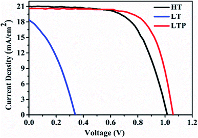
In our study, we employed a planar heterojunction (FTO/SnO2/MAPbI3/Spiro-OMeTAD/Ag) based PSC architecture. To investigate the effect of oxygen plasma treatment on the performance of PSCs based on LT-SnO2, we fabricated three different sets of PSCs with the aforementioned structure. The main difference among the three sets is post-treatment of the SnO2 layers. In the case of the pristine LT-SnO2-based PSC, SnO2 was only annealed at 150 °C, whereas oxygen plasma was directly performed on the LT-SnO2 for the LTP-SnO2-based PSC. For comparison, we also fabricated a conventional HT-SnO2-based PSC by annealing SnO2 at 200 °C.Fig. 1 shows the current density–voltage curve (J–V curve) for champion cells based on LT-SnO2, LTP-SnO2, and HT-SnO2. PSC fabricated using LT-SnO2 generated a PCE of 2.27% with Voc of 0.34 V, short-circuit current density (Jsc) of 18.44 mA cm−2, and fill factor (FF) of 0.36. Fascinatingly, after oxygen plasma treatment on LT-SnO2, the performance of PSC is drastically improved with PCE, Voc, Jsc, and FF values of 15.30%, 1.06 V, 20.58 mA cm−2, and 0.70, respectively. Moreover, the PSC based on LTP-SnO2 has a higher PCE than that of the conventionally annealed HT-SnO2-based PSC, 13.52%. The device parameters are listed in Table 1. The LT-SnO2-based PSC exhibited inferior performance due to the incomplete precursor-to-metal oxide conversion affecting the interface between MAPbI3 and ETL, as foreseen by the shallow slope of the J–V curve.28 Plasma treatment effectively modifies the surface of LT-SnO2, facilitating metal oxide formation and improving the growth property of the subsequent perovskite layer. This result indicates that it is possible to fabricate SnO2 ETL at a low temperature using oxygen plasma.
| Device | Jsc (mA cm−2) | Voc (V) | Fill factor | Efficiency (%) |
|---|---|---|---|---|
| HT-SnO2 | 21.02 | 1.02 | 0.63 | 13.52 |
| LT-SnO2 | 18.44 | 0.34 | 0.36 | 2.27 |
| LTP-SnO2 | 20.58 | 1.06 | 0.70 | 15.30 |
A statistical distribution for all three types of PSC is obtained to investigate the reproducibility of the fabrication process, as shown in Fig. 2, and the corresponding device parameters are listed in Table S1.† The average PCE of the LTP-SnO2-based PSC is 14.16%, which is higher than that of the LT-SnO2- and HT-SnO2-based PSCs. All the device parameters of the LTP-SnO2-based PSC show smaller deviations, which indicate that oxygen plasma treatment is a consistent and reproducible process.
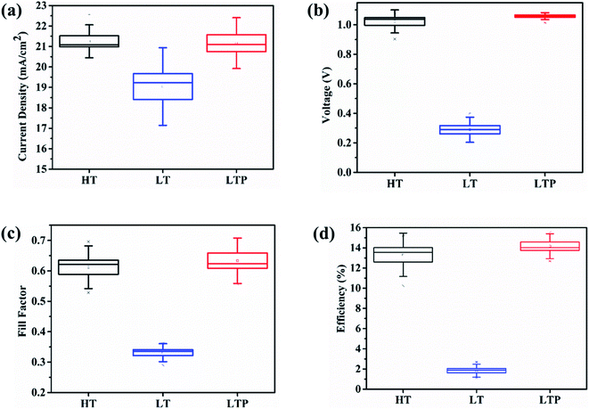 | ||
| Fig. 2 Statistical distribution of PSCs fabricated with HT-, LT-, and LTP-SnO2. (a) Jsc (b) Voc (c) fill factor (d) efficiency. | ||
The above experimental results demonstrate that oxygen plasma treatment is sufficiently effective to improve the performance of LT-SnO2-based PSCs. In addition, a series of experiments were conducted at various annealing temperatures ranging from 100 °C to 150 °C to ascertain that oxygen plasma treatment is also valid for lower annealing temperatures under 150 °C (Fig. S1 and Table S2†). The efficiency of the LT-SnO2-based PSCs significantly increased, even at an annealing temperature of 100 °C, with oxygen plasma treatment, and the highest efficiency was obtained at 150 °C. Although the efficiency of LTP-SnO2-based PSCs increased as the annealing temperature increased, it was confirmed that the oxygen plasma treatment was still effective in improving the efficiency of PSCs at much lower temperatures. Furthermore, the efficiency of the LTP-SnO2 PSC annealed at 125 °C was comparable to that of HT-SnO2 PSC, revealing that the fabrication temperature achieved with oxygen plasma treatment is compatible with most plastic substrates.
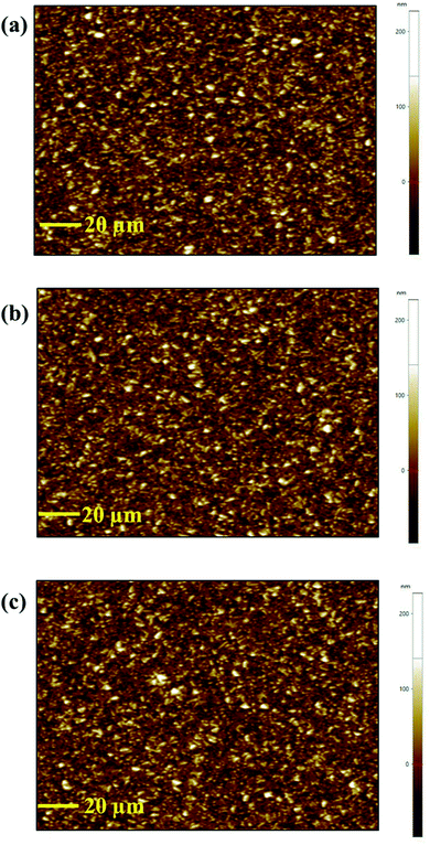
First, to elucidate the causes of enhancement in photovoltaic performance via oxygen plasma treatment, we investigated the compositional and structural changes in SnO2 ETL by XPS, XRD, and AFM. As shown in Fig. S3,† XRD analysis was performed for LTP-, LT-, and HT-SnO2. As expected, the SnO2 layers are amorphous with no visible diffraction peaks, irrespective of post-treatment conditions, because a high temperature of 450 °C is required for the formation of the SnO2 crystalline structure.29,30 Fig. 3 shows the AFM images of HT-, LT-, and LTP-SnO2. All the SnO2 films based on different post-treatment conditions resulted in a uniform surface with a root-mean-square roughness value of ∼34 nm. Oxygen plasma treatment on the SnO2 surface does not significantly affect the surface morphology of SnO2. However, oxygen plasma on LT-SnO2 improved its hydrophilicity, as determined by CA measurement (Fig. S4†). The low surface energy of LT-SnO2 (CA of 63.78°) reduces the uniform coverage of MAPbI3 on its surface, which affects the performance of the PSC. The improved wettability of LTP-SnO2 enhances the interface characteristics between the ETL and perovskite layer. Fig. 4 shows the XPS spectra of the Sn, O, and Cl peaks for the LT- and LTP-SnO2 layers. Both LT- and LTP-SnO2 films exhibited two peaks at binding energies of 487.3 and 495.7 eV corresponding to Sn 3d5/2 and Sn 3d3/2, as previously reported.31 The single peak at 487.3 eV is assigned to the Sn4+ oxidation state of SnO2. However, there is no visible peak at the binding energy of 485.8 eV that corresponds to the Sn2+ oxidation state which indicates the formation of SnO. At a low temperature, the reaction involved in the formation of SnO2 might occur via an indirect pathway that produces an intermediate product Sn(OH)2 because of the reaction of SnCl2 with C2H5OH as given in the above reaction equation. This intermediate product is converted into SnO which further reacts to form SnO2.32 Therefore, a single peak at the 487.3 eV reveals that SnO2 begun to form at a low temperature of 150 °C. The XPS peak of O 1s were deconvoluted into two peaks, where a peak at a binding energy of 531.1 eV corresponds to the lattice oxygen atoms that confirms the formation of SnO2.24 The peak at the binding energy of 532.2 eV represents hydroxide species.33 After undergoing oxygen plasma, the –OH group of LT-SnO2 decreased slightly, indicating that oxygen plasma helps in the breakage of the –OH bond and initiates the formation of SnO2.13 The most noticeable difference that arises in the XPS spectra from plasma treatment is the detection of Cl−, as shown in Fig. 4b. The Cl− peak originates from the utilization of SnCl2·2H2O precursor to fabricate the SnO2 ETL. As can be observed, LT-SnO2 has high-intensity Cl 2p peaks that indicate the presence of residual Cl−. After oxygen plasma treatment, the Cl 2p level gradually decreased, representing the minimal presence of metal chloride precursor. This means that oxygen plasma improves the conversion of the precursor to metal oxide, as described in the above equation.
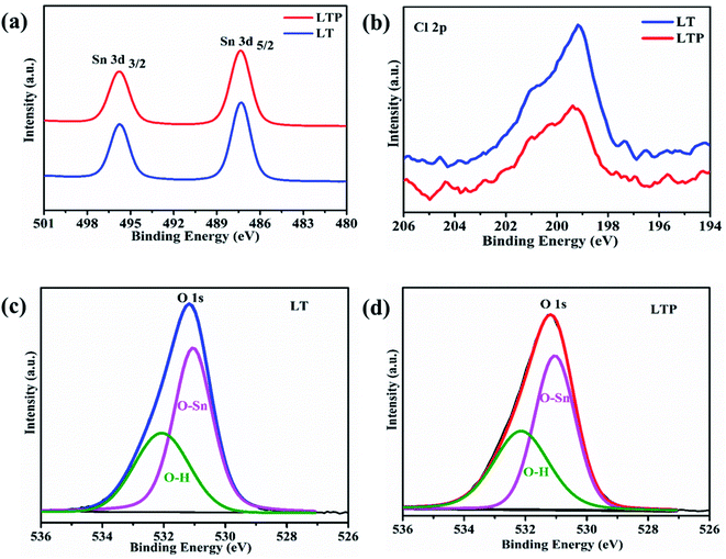 | ||
| Fig. 4 XPS spectra of (a) Sn 3d, (b) Cl 2p from LT- and LTP-SnO2. (c) and (d) O 1s from LT- and LTP-SnO2, respectively. | ||
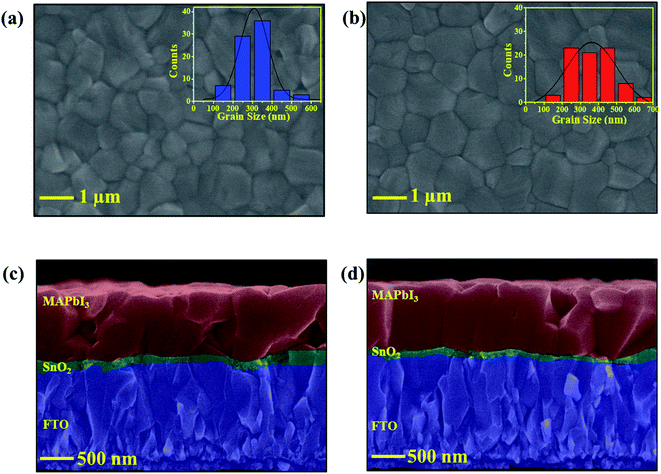
Second, to investigate the improvement in the performance of oxygen plasma-treated PSCs, the structural and morphological changes in the MAPbI3 layer were examined. The XRD patterns of the MAPbI3 layer on LT-, HT-, and LTP-SnO2 are displayed in Fig. S5.† The samples based on different ETL conditions exhibit diffraction peaks at 14.08°, 20.0°, 23.54°, 24.5°, 28.4°, 31.9°, 34.9°, 40.5°, and 43.2° corresponding to the (110), (112), (211), (202), (220), (222), (312), (224), and (314) planes, respectively, which confirms the formation of a tetrahedral MAPbI3 structure.34 There are no noticeable differences in the crystalline nature of the MAPbI3 layer for HT-, LT-, and LTP-SnO2. This reveals that oxygen plasma treatment does not affect the crystalline nature of the perovskite layer. Fig. 5 and S7† show the top view SEM image and cross sectional SEM image of the perovskite film deposited on LT-SnO2 and LTP-SnO2. The surface morphology of MAPbI3 on HT-, LT-, and LTP-SnO2 is uniform, dense, and homogeneous with pinhole-free structures. The average grain size of the perovskite film for LTP-SnO2 is 314.38 nm, which is greater than those of HT-SnO2 and LT-SnO2 with values of 280.33 and 255.68 nm, respectively. It is generally accepted that a MAPbI3 grain size of 300–500 nm is beneficial for charge transportation on PSC.16,35 The large grain size in LTP-SnO2 is obtained because oxygen plasma improves the wettability of the surface, as indicated by the low CA. This small CA reduces the Gibbs free energy for heterogeneous nucleation, which assists the nucleation process that leads to improved grain size.36 This improved grain size reduces the interface defect states that sequentially suppress the charge recombination at the grain boundaries, thus leading to improved PCE for oxygen plasma-treated PSCs. The reduced grain size in LT-SnO2 is also responsible for its lower Voc, as indicated by the J–V graph, because of the high charge trap sites within the grain boundaries.15
To further investigate the role of oxygen plasma treatment on the interfacial transfer kinetics between the ETL and perovskite layer, we analyzed the steady-state PL spectra and TRPL decay on the HT-SnO2/MAPbI3, LT-SnO2/MAPbI3, and LTP-SnO2/MAPbI3 films, as shown in Fig. 6. The peak at 770 nm corresponds to the fluorescence emission originating from the MAPbI3 layer.4 The PL intensity of perovskite on LTP-SnO2 is strongly quenched compared to that of MAPbI3 deposited on HT-SnO2 and LT-SnO2. This indicates that efficient electron extraction and transportation from MAPbI3 to the LTP-SnO2 layer subdues the nonradiative recombination at the interface. Fig. 6b illustrates the TRPL decay profiles of the perovskite layer on the HT-SnO2, LT-SnO2, and LTP-SnO2 samples. The corresponding τ values were determined by fitting the data with tri-exponential decay functions, and the values are represented in Table S3.† The value of τ1, τ2, and τ3 correspond to the decay time of fast, intermediate, and slow component respectively. Fast decay components correspond to an effective charge extraction from perovskite to the ETL layer, whereas τ2 and τ3 represent the radiative recombination of free carriers.37,38 In addition, the LTP-SnO2 sample exhibits a low PL decay time (τ1 = 2.28, τ2 = 7.24) compared to LT-SnO2 (τ1 = 2.48, τ2 = 11.5), indicating an effective electron transfer from the perovskite to ETL. The average recombination lifetime (τavg) is calculated using the equation below:
 | ||
| Fig. 6 (a) Steady state PL spectra and (b) TRPL spectra of MAPbI3 deposited on HT-, LT-, and LTP-SnO2. | ||
To more accurately examine the differences in the carrier transport and recombination dynamics at SnO2 ETL/MAPbI3 interfaces, electrochemical impedance spectroscopy (EIS) is performed. Fig. 7 shows the Nyquist plot obtained by EIS for three different PSCs measured under the dark condition at a bias voltage of 0.9 V. The solid lines in the graph represent the fitted results of the experimental data based on the equivalent circuit model shown in Fig. 7c. The values of the fitted parameters are given in Table S4.† The EIS spectra of all three devices have one arc that represents the interfacial recombination resistance (Rrec), which is inversely proportional to the recombination rate of the charge carriers.13,39 The larger arc of the LTP-SnO2 corresponds to a higher Rrec, which indicates a smaller recombination constant (Krec) in solar cells. The Rrec of LTP-SnO2, 3669 Ω, is higher than those of HT-SnO2 and LT-SnO2, 1961 and 19.37 Ω, respectively. Higher Rrec values indicate that the device exhibits a low leakage current and reduced charge recombination at the ETL/MAPbI3 interface.40 In addition, we can interpolate the series resistance (Rs) from the EIS spectra at the starting point of the real part of the Nyquist plot.9 The Rs value of LTP-SnO2 is 19.69 Ω, which is lower than those of HT-SnO2 and LT-SnO2, which are 25.43 and 30.95 Ω, respectively. The only differences during device fabrication lie in the post-treatment of ETL; therefore, the small Rs and higher Rrec values of LTP-SnO2 convey that oxygen plasma treatment on LT-SnO2 is advantageous for efficient electron extraction, which is in agreement with the PL results. All the results based on PL, TRPL, and EIS are consistent with the PCE of the PSC for LTP-SnO2 ETL.
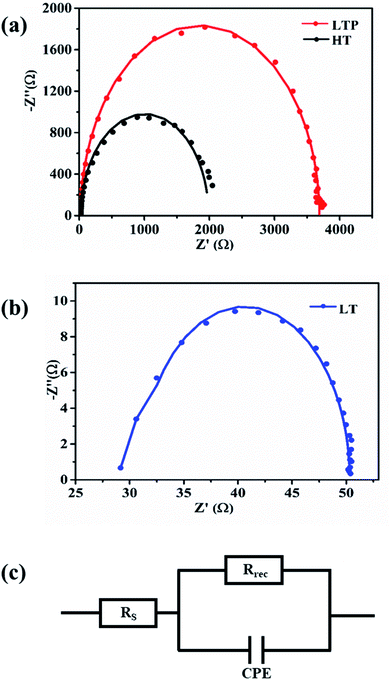 | ||
| Fig. 7 Nyquist plots of perovskite solar cells based on (a) HT-SnO2 and LTP-SnO2, (b) LT-SnO2, (c) equivalent circuit model. | ||
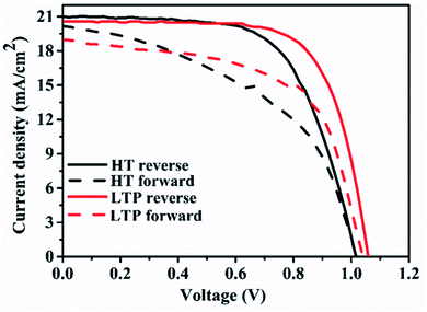
Fig. 8 displays the J–V hysteresis of HT-SnO2 and LTP-SnO2 PSC by sweeping the forward and reverse scan directions. The value of the hysteresis index (HI) is determined from the following equation:41
| HI = JRS (0.8Voc) − JFS (0.8Voc)/JRS (0.8Voc), |
4. Conclusion
Interface engineering of a low-temperature deposited SnO2 film surface using oxygen plasma treatment improves the performance of PSCs. Oxygen plasma improves the conversion of the precursor-to-metal oxide layer. This effectively improves the hydrophilicity of LT-SnO2, which enhances the surface coverage of the MAPbI3 layer. The increased MAPbI3 grain size of LTP-SnO2 resulted in an improvement in Voc from 0.34 V to 1.06 V after plasma treatment. Surface treatment by oxygen plasma does not affect the structural properties of the perovskite layer that is deposited on the top but leads to efficient electron extraction from the perovskite layer to the ETL. Further oxygen plasma effectively increased the recombination resistance at the ETL/perovskite interface and led to an efficiency of 15.30%. In this work, we studied the impact of oxygen plasma treatment in the structural, compositional, and morphological behaviors of SnO2 and MAPbI3. The results indicate that oxygen plasma treatment is effective for fabricating SnO2-based PSCs for future flexible applications.Author contributions
The manuscript was written through contributions of all authors. All authors have given approval to the final version of the manuscript.Conflicts of interest
The authors declare no competing financial interest.Acknowledgements
This work was supported by the National Research Foundation (NRF) grant funded by the Korea government (MSIT) (2020R1F1A1074743 and 2021R1A4A1031761).References
- J. Jeong, M. Kim, J. Seo, H. Lu, P. Ahlawat, A. Mishra, Y. Yang, M. A. Hope, F. T. Eickemeyer, M. Kim, Y. J. Yoon, I. W. Choi, B. P. Darwich, S. J. Choi, Y. Jo, J. H. Lee, B. Walker, S. M. Zakeeruddin, L. Emsley, U. Rothlisberger, A. Hagfeldt, D. S. Kim, M. Grätzel and J. Y. Kim, Nature, 2021, 592, 381–385 CrossRef CAS PubMed.
- H. Lu, A. Krishna, S. M. Zakeeruddin, M. Grätzel and A. Hagfeldt, iScience, 2020, 23, 1–14 Search PubMed.
- L. Xiong, J. Li, F. Ye, H. Wang, Y. Guo, X. Ming, Q. Chen, S. Zhang, R. Xie, Z. Chen, Y. Lv, G. Hu, Y. He and G. Fang, Adv. Funct. Mater., 2021, 31, 2–11 Search PubMed.
- C. Chen, Y. Jiang, J. Guo, X. Wu, W. Zhang, S. Wu, X. Gao, X. Hu, Q. Wang, G. Zhou, Y. Chen, J. M. Liu, K. Kempa and J. Gao, Adv. Funct. Mater., 2019, 29, 1–9 Search PubMed.
- X. Yin, Z. Song, Z. Li and W. Tang, Energy Environ. Sci., 2020, 13, 4057–4086 RSC.
- S. Mabrouk, B. Bahrami, H. Elbohy, K. M. Reza, A. Gurung, M. Liang, F. Wu, M. Wang, S. Yang and Q. Qiao, InfoMat, 2020, 2, 928–941 CrossRef CAS.
- M. Shekargoftar, J. Pospisil, M. Kratochvíl, J. Vida, P. Souček and T. Homola, Energy Technol., 2021, 9(5), 2001076 CrossRef CAS.
- P. F. Méndez, S. K. M. Muhammed, E. M. Barea, S. Masi and I. Mora-Seró, Sol. RRL, 2019, 3(9), 1900191 CrossRef.
- J. Song, E. Zheng, X. F. Wang, W. Tian and T. Miyasaka, Sol. Energy Mater. Sol. Cells, 2016, 144, 623–630 CrossRef CAS.
- A. S. R. Bati, M. Hao, T. J. Macdonald, M. Batmunkh, Y. Yamauchi, L. Wang and J. G. Shapter, Small, 2021, 17, 1–9 CrossRef PubMed.
- J. Ma, J. Su, Z. Lin, L. Zhou, J. He, J. Zhang, S. Liu, J. Chang and Y. Hao, Nano Energy, 2020, 67, 104241 CrossRef CAS.
- C. Zhang, Y. Shi, S. Wang, Q. Dong, Y. Feng, L. Wang, K. Wang, Y. Shao, Y. Liu and S. Wang, J. Mater. Chem. A, 2018, 6, 17882–17888 RSC.
- H. B. Lee, N. Kumar, M. M. Ovhal, Y. J. Kim, Y. M. Song and J. W. Kang, Adv. Funct. Mater., 2020, 30, 1–12 Search PubMed.
- X. Huang, Z. Hu, J. Xu, P. Wang, L. Wang, J. Zhang and Y. Zhu, Sol. Energy Mater. Sol. Cells, 2017, 164, 87–92 CrossRef CAS.
- M. Park, J. Y. Kim, H. J. Son, C. H. Lee, S. S. Jang and M. J. Ko, Nano Energy, 2016, 26, 208–215 CrossRef CAS.
- N. Zhu, X. Qi, Y. Zhang, G. Liu, C. Wu, D. Wang, X. Guo, W. Luo, X. Li, H. Hu, Z. Chen, L. Xiao and B. Qu, ACS Appl. Energy Mater., 2019, 2, 3676–3682 CrossRef CAS.
- J. Song, E. Zheng, J. Bian, X. F. Wang, W. Tian, Y. Sanehira and T. Miyasaka, J. Mater. Chem. A, 2015, 3, 10837–10844 RSC.
- W. Ke, G. Fang, Q. Liu, L. Xiong, P. Qin, H. Tao, J. Wang, H. Lei, B. Li, J. Wan, G. Yang and Y. Yan, J. Am. Chem. Soc., 2015, 137, 6730–6733 CrossRef CAS PubMed.
- E. H. Anaraki, A. Kermanpur, L. Steier, K. Domanski, T. Matsui, W. Tress, M. Saliba, A. Abate, M. Grätzel, A. Hagfeldt and J. P. Correa-Baena, Energy Environ. Sci., 2016, 9, 3128–3134 RSC.
- G. Murugadoss, H. Kanda, S. Tanaka, H. Nishino, S. Ito, H. Imahoric and T. Umeyama, J. Power Sources, 2016, 307, 891–897 CrossRef CAS.
- X. Ren, D. Yang, Z. Yang, J. Feng, X. Zhu, J. Niu, Y. Liu, W. Zhao and S. F. Liu, ACS Appl. Mater. Interfaces, 2017, 9, 2421–2429 CrossRef CAS PubMed.
- X. Ren, Y. Liu, D. G. Lee, W. Bin Kim, G. S. Han, H. S. Jung and S. (Frank) Liu, InfoMat, 2020, 2, 401–408 CrossRef CAS.
- B. Kan, Y. Kan, L. Zuo, X. Shi and K. Gao, InfoMat, 2021, 3, 175–200 CrossRef CAS.
- L. Huang, X. Sun, C. Li, J. Xu, R. Xu, Y. Du, J. Ni, H. Cai, J. Li, Z. Hu and J. Zhang, ACS Appl. Mater. Interfaces, 2017, 9, 21909–21920 CrossRef CAS PubMed.
- M. Zhu, W. Liu, W. Ke, S. Clark, E. B. Secor, T. Bin Song, M. G. Kanatzidis, X. Li and M. C. Hersam, J. Mater. Chem. A, 2017, 5, 24110–24115 RSC.
- V. H. Tran, R. B. Ambade, S. B. Ambade, S. H. Lee and I. H. Lee, ACS Appl. Mater. Interfaces, 2017, 9, 1645–1653 CrossRef CAS PubMed.
- J. Nam, I. Nam, E. J. Song, J. D. Kwon, J. Kim, C. S. Kim and S. Jo, Nanomaterials, 2019, 9, 1–10 CrossRef CAS PubMed.
- A. S. Subbiah, N. Mathews, S. Mhaisalkar and S. K. Sarkar, ACS Energy Lett., 2018, 3, 1482–1491 CrossRef CAS.
- M. F. M. Noh, M. F. Soh, C. H. Teh, E. L. Lim, C. C. Yap, M. A. Ibrahim, N. A. Ludin and M. A. M. Teridi, Sol. Energy, 2017, 158, 474–482 CrossRef CAS.
- O. Kassem, M. Saadaoui, M. Rieu and J.-P. Viricelle, Proceedings, 2017, 1, 622 CrossRef.
- R. G. Motsoeneng, I. Kortidis, S. S. Ray and D. E. Motaung, ACS Omega, 2019, 4, 13696–13709 CrossRef CAS PubMed.
- M. F. Mohamad Noh, N. A. Arzaee, J. Safaei, N. A. Mohamed, H. P. Kim, A. R. Mohd Yusoff, J. Jang and M. A. Mat Teridi, J. Alloys Compd., 2019, 773, 997–1008 CrossRef CAS.
- Y. Gao, Y. Masuda and K. Koumoto, Langmuir, 2004, 20, 3188–3194 CrossRef CAS PubMed.
- J. Nam, J. H. Kim, C. S. Kim, J. D. Kwon and S. Jo, ACS Appl. Mater. Interfaces, 2020, 12, 12648–12655 CrossRef CAS PubMed.
- B. Liu, S. Wang, Z. Ma, J. Ma, R. Ma and C. Wang, Appl. Surf. Sci., 2019, 467–468, 708–714 CrossRef CAS.
- D. Yang, R. Yang, K. Wang, C. Wu, X. Zhu, J. Feng, X. Ren, G. Fang, S. Priya and S. (Frank) Liu, Nat. Commun., 2018, 9, 3239 CrossRef PubMed.
- Y. Liu, H. Lu, J. Niu, H. Zhang, S. Lou, C. Gao, Y. Zhan, X. Zhang, Q. Jin and L. Zheng, AIP Adv., 2018, 8(9), 095108 CrossRef.
- J. Xing, C. Zhao, Y. Zou, W. Kong, Z. Yu, Y. Shan, Q. Dong, D. Zhou, W. Yu and C. Guo, Light: Sci. Appl., 2020, 9, 111 CrossRef CAS PubMed.
- Y. Li, C. Feng, H. Cheng and Z. S. Wang, Sol. RRL, 2018, 2, 1–8 CrossRef.
- R. Xu, Y. Li, S. Feng, J. Wang, J. Zhang, X. Zhang, C. Bian, W. Fu, Z. Li and H. Yang, J. Mater. Sci., 2020, 55, 5681–5689 CrossRef CAS.
- H.-S. Kim and N.-G. Park, J. Phys. Chem. Lett., 2014, 5, 3434 CrossRef CAS PubMed.
Footnote |
| † Electronic supplementary information (ESI) available: J–V curves of perovskite solar cells; XRD and XPS analysis of SnO2; XRD and SEM analysis of MAPbI3; contact angle images of water droplet on SnO2; device parameters of perovskite solar cells. See DOI: 10.1039/d1ra08946c |
| This journal is © The Royal Society of Chemistry 2022 |

