 Open Access Article
High-throughput growth of HfO2 films using temperature-gradient laser chemical vapor deposition†
Rong Tu ab,
Ziming Liub,
Chongjie Wangb,
Pengjian Lubc,
Bingjian Guode,
Qingfang Xub,
Bao-Wen Li
 d and
Song Zhang
 *b
*b
aChaozhou Branch of Chemistry and Chemical Engineering Guangdong Laboratory, Chaozhou 521000, People's Republic of China
bState Key Laboratory of Advanced Technology for Materials and Processing, Wuhan University of Technology, 122 Luoshi Road, Wuhan 430070, People's Republic of China. E-mail: kobe@whut.edu.cn; Fax: +86-27-87499449; Tel: +86-27-87499449
cWuhan Tuocai Technology Co., Ltd., 147 Luoshi Road, Wuhan 430070, People's Republic of China
dSchool of Materials Science and Engineering, Wuhan University of Technology, 122 Luoshi Road, Wuhan 430070, People's Republic of China
eZhejiang MTCN Technology Co., Ltd., No. 59, Luhui Road, Taihu Street, Zhejiang Province 311103, People's Republic of China
First published on 23rd May 2022
Abstract
The use of hafnia (HfO2) has facilitated recent advances in high-density microchips. However, the low deposition rate, poor controllability, and lack of systematic research on the growth mechanism limit the fabrication efficiency and further development of HfO2 films. In this study, the high-throughput growth of HfO2 films was realized via laser chemical vapor deposition using a laser spot with a large gradient temperature distribution (100 K mm−1), in order to improve the experimental efficiency and controllability of the entire process. HfO2 films fabricated by a single growth process could be divided into four regions with different morphologies, and discerned for deposition temperatures increasing from 1300 K to 1600 K. The maximum deposition rate reached 362 μm h−1, which was 102 to 104 times higher than that obtained using existing deposition methods. The dielectric constants of high-throughput HfO2 films were in the range of 16–22, which satisfied the demand of replacing the traditional SiO2 layer for a new generation of microchips.
1. Introduction
High-density microchips offer the advantages of a compact size, adaptive integration, and massive parallelization. Meanwhile, corresponding advances are required in dielectric materials to passivate exposed surfaces against destabilization related to ion transport and in barrier materials to protect core components against thermal shock or fluid erosion in harsh operating environments.1,2 In 2007, Intel Inc. announced that HfO2, a high-k inorganic material with an ultrahigh melting point (3085 K), a sufficient electrical breakdown field (3.9–6.7 MV cm−1), low thermal conductivity (∼2.55 W K−1 m−1), and four times the density (9.68 g cm−3) of SiO2 (2.26 g cm−3), was the most promising dielectric layer material to replace the traditional SiO2 layer for a new generation of microchips.3–7However, HfO2 films have disadvantages of the low growth rate, poor controllability, and high preparation cost, resulting in a lack of systematic research on the growth mechanism. Table 1 shows the deposition temperature (Tdep), deposition rate (Rdep), and thickness (d) measured for HfO2 films grown using different methods, such as metal–organic CVD (MOCVD),8–12 thermal CVD (TCVD),13 atomic layer deposition (ALD),14–18 sol–gel,19–21 radio frequency magnetron sputtering (RFMS),22 and pulsed laser deposition (PLD).23 As a result of the low deposition rate of HfO2 films, most scholars have studied the growth of films with thicknesses below 100 nm over the last decade, such that HfO2 films have not been exploited at the micron scale. In order to significantly improve the CVD deposition rates, our group has been developing LCVD since 2012,24 and we have been able to rapidly grow SiC,25 SiOC,26 AlN,27 LiAlO2,28 BaTi2O5,29 and SmBa2Cu3O7 (ref. 30) films at deposition rates 101 to 104 times higher than those of conventional CVD methods. In addition, novel structures and growth mechanisms have been found using LCVD to grow films in previous studies.25,26,31
| Ref. | Method | Precursor | Tdep (K) | Rdep (μm h−1) | d (nm) |
|---|---|---|---|---|---|
| 8 | MOCVD | Cp2Hf(NEt2)2 | 1273 | 2.40 × 10⁻¹ | 84 |
| 9 | MOCVD | (Cp2CMe2)HfMe2 | 923 | 7.20 × 10⁻² | 25 |
| 10 | MOCVD | Hf(dmml)4 | 973 | 5.40 × 10⁻² | 20 |
| 11 | MOCVD | Hf(mp)4 | 873 | 1.62 × 10⁻¹ | 4.1 |
| 12 | MOCVD | HfOtBu(NEtMe)3 | 873 | 4.80 × 10⁻¹ | 19 |
| 13 | TCVD | HfCl4 | 473 | 1.64 × 10⁻³ | 59 |
| 14 | ALD | Hf(NMe2)4 | 1373 | 9.60 × 10⁻³ | 3.4 |
| 15 | ALD | HfOtBu(NEtMe)3 | 623 | 8.90 × 10⁻² | 13 |
| 16 | ALD | Hf(NEtMe)4 | 633 | 1.01 × 10⁻² | 4.0 |
| 17 | ALD | Hf(NMe2)4 | 1273 | 8.64 × 10⁻² | 3.5 |
| 18 | ALD | CpHf(NMe2)3 | 523 | 7.20 × 10⁻² | 15 |
| 19 | Sol–gel | HfCl4 | 873 | 1.03 × 10⁻³ | 3.1 |
| 20 | Sol–gel | HfCl4 | 823 | 2.07 × 10⁻³ | 2.0 |
| 21 | Sol–gel | HfCl4 | 873 | 6.67 × 10⁻³ | 3.0 |
| 22 | RFMS | HfO2 target | 573 | 7.50 × 10⁻² | 25 |
| 23 | PLD | HfO2 target | 1173 | 8.52 × 10⁻¹ | 17 |
| This study | HT-LCVD | Hf(acac)4 | 1300–1600 | 4.68 × 101 to 3.62 × 10² | 7.8× 10³ to 6.0 × 10⁴ |
Moreover, in order to further improve the efficiency and controllability of LCVD, the high-throughput growth was introduced for analyzing the evolution of growth mechanisms. Because the high-throughput growth offers a significant advantage in fabricating multiple specimens from only a single preparation. It is able to shorten the experimental period and fabricate samples under the continuous conditions.32 However, various factors in CVD processes, such as the growth temperature, pressures, and gas flow rates, increase the difficulty of experiments in high-throughput HfO2 films.33 The presence of multiple variables results in an extended experimental time and reduces the repeatability of the entire process; hence, little pertinent research has been performed on high-throughput CVD.
In this study, HfO2 films were grown using a highly efficient HT-LCVD process, achieving a stable control of large gradient (100 K mm−1) temperature fields. We significantly shortened the experimental time by modifying the high-throughput LCVD (HT-LCVD) method by using a temperature-gradient preparation with credible measurements and repeatability, resulting in 102 to 104 times higher growth rates than other methods and the fabrication of multiple specimens per unit time. And four novel gradient microstructures appeared simultaneously on a high-throughput sample. Their morphologies, deposition rates, dielectric constants, and growth mechanisms were determined.
2. Experimental section
Fig. S1† shows the HT-LCVD apparatus that was constructed to fabricate HfO2 films. An InGaAlAs beam-by-diode laser (wavelength: 808 nm, LHTC-200, ZK-LASER, China) was introduced into the chamber through a quartz-glass window and diverged by an optical lens (around 18 mm in diameter) to irradiate the entire substrate surface. The diode laser beam created a temperature-gradient distribution over the substrate surface. Fig. 1 shows vertical and stereo views of the temperature distribution during the high-throughput growth. As Tdep increased from 1300 K to 1600 K, the HfO2 film with different novel microstructures could be observed in four specific regions. The temperature distribution was measured by an infrared pyrometer (CHINO IR-AH) and regulated by an infrared temperature-measurement program (OMRON, Japan). The program was based on the LabVIEW 8.5 Virtual Instrument engineering platform (NI, USA), and used to measure the temperature distribution within the entire substrate surface, adjusting the laser power to stabilize the temperature field automatically. Fig. S2† shows the growth procedure. Si (100) single crystal wafers were cut into samples with dimensions of 10.0 × 10.0 × 0.5 mm for use as substrates, which were placed on a heating stage in the chamber and preheated at 873 K for 5 min after evacuating the chamber to 5 Pa. The substrate holder was supported by an alumina plate with a K-type thermocouple, which was used to monitor the temperature of the heating stage. The precursor, Hf(acac)4 (Aladdin Inc., Shanghai, China), was vaporized at 493 K and carried into the vacuum chamber by Ar gas (99.999%). Table 2 shows a summarization of deposition conditions used to prepare the temperature-gradient HfO2 films via HT-LCVD.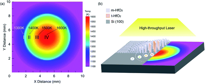 | ||
| Fig. 1 (a) Top view of the temperature distribution and (b) stereo view in the four discernible regions. | ||
| Precursor | Hf(acac)4 |
| Substrate | Si (100) |
| Deposition temperature (Tdep) | 1250–1600 K |
| Total pressure (Ptot) | 200 Pa |
| Laser power (PL) | 100 W |
| Precursor vaporization temperature | 493 K |
| Pipe/gas nozzle temperature (Tpip) | 573 K |
| Deposition time (tdep) | 10 min |
| Ar carrier gas flow rate | 1.67 × 10⁻⁶ m3 s−1 (100 sccm) |
| Ar diluent gas flow rate | 1.67 × 10⁻⁶ m3 s−1 (100 sccm) |
| Nozzle diameter | 6.0 mm |
| Distance between nozzle and substrate | 15 mm |
The crystalline phases were examined by the micro X-ray diffraction (μ-XRD; D8 DISCOVER, Bruker, Germany; 40 kV, 40 mA) with Cu Kα2 radiation, whereby a small region (0.4 mm in diameter) in the specimen was analyzed. The composition of the micro areas on the surface was detected by Raman spectroscopy (inVia Renishaw, 633 nm He–Ne laser, UK). The surface and cross-section morphologies were characterized by scanning electron microscopy (SEM, Quanta FEG 450, FEI, USA, at 20 kV). The microstructures were observed using double-beam electron microscopy with focused ion beam processing (FIB, Helios NanoLab G3 UC, FEI, USA, at 20 kV) and transmission electron microscopy (TEM, JEOL Ltd., Japan, JEM-2100F, at 200 kV). The complex permittivity and dielectric loss of the HfO2 films in four regions were measured by Leakage Inductance–Capacitance–Resistance dielectric tester (LCR, Agilent E4980A, Radiant, USA).
3. Results and discussion
Fig. 2(a)–(d) displays the μ-XRD patterns of a high-throughput HfO2 film in four temperature regions. The (![[1 with combining macron]](https://www.rsc.org/images/entities/char_0031_0304.gif) 11) and (111) main peaks of m-HfO2 at 2θ = 28.3° and 31.7°, respectively, were identified for all specimens. At Tdep = 1400 K, m-HfO2 exhibited a strong 〈002〉 orientation. The two diffraction peaks at 2θ = 34.6° and 72.7° corresponded to the (002) and (004) planes of m-HfO2, respectively. The patterns for the HfO2 film in Regions III (1500 K) and IV (1600 K) exhibited two prominent peaks at 2θ = 30.1° and 35.1° corresponding to the (
11) and (111) main peaks of m-HfO2 at 2θ = 28.3° and 31.7°, respectively, were identified for all specimens. At Tdep = 1400 K, m-HfO2 exhibited a strong 〈002〉 orientation. The two diffraction peaks at 2θ = 34.6° and 72.7° corresponded to the (002) and (004) planes of m-HfO2, respectively. The patterns for the HfO2 film in Regions III (1500 K) and IV (1600 K) exhibited two prominent peaks at 2θ = 30.1° and 35.1° corresponding to the (![[1 with combining macron]](https://www.rsc.org/images/entities/char_0031_0304.gif) 11) and (111) planes of t-HfO2, respectively, indicating the coexistence of m- and t-HfO2.
11) and (111) planes of t-HfO2, respectively, indicating the coexistence of m- and t-HfO2.
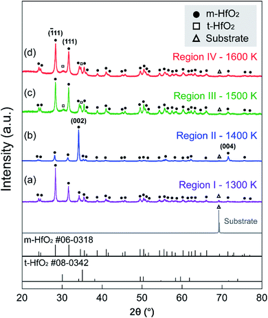 | ||
| Fig. 2 μ-XRD patterns of the HfO2 film in different regions produced by the high-throughput growth process: (a) 1300 K/I, (b) 1400 K/II, (c) 1500 K/III, and (d) 1600 K/IV. | ||
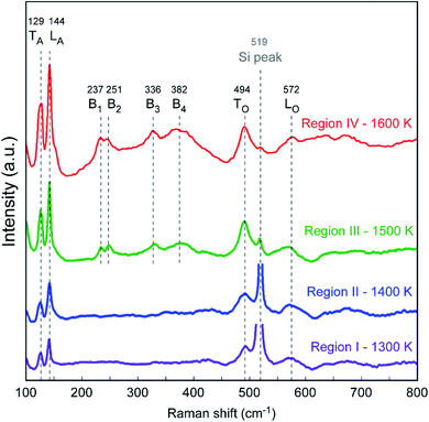
Fig. 3 shows the Raman scattering spectra for the HfO2 film in the four regions with deposition temperatures of 1300–1600 K. For Raman shifts from 100 to 800 cm−1, the two characteristic peaks at ∼129 cm−1 and ∼144 cm−1 were ascribed to two acoustic phonon modes for transverse acoustic (TA) and longitudinal acoustic (LA) phonons of m-HfO2 films, respectively.34 The intensity of the acoustic-phonon peaks increased remarkably with the film thickness. Two characteristic bands appeared at approximately 494 cm−1 and 572 cm−1 for all samples that were ascribed to transverse optical (TO) and longitudinal optical (LO) phonons, respectively. Fig. 4(b) shows the intensity ratio between TO and LO bands, η, that was used to evaluate the crystallinity of HfO2 films. When Tdep increased from 1300 K to 1600 K, the lowest η was observed at 1400 K (Region II). A similar trend is observed for the full width at half maximum (FWHM) of the m-HfO2 (111) peaks in μ-XRD patterns shown in Fig. 4(a). Tkachev et al.35 analyzed the XRD patterns and Raman spectra of polycrystalline HfO2 films with various grain sizes, and found that η for the Raman spectra decreased as the grain size increased. Hence, we inferred that the increase in the crystallinity of HfO2 films in different regions resulted from an increase in the proportion of large grains. For Tdep above 1500 K (Regions III and IV), the four broad peaks (B1–B4) at ∼237, ∼251, ∼336, and ∼382 cm−1 in the spectra were ascribed to the existence of the tetragonal phase. The peaks at 519 cm−1 were assigned to the Si (100) substrates.
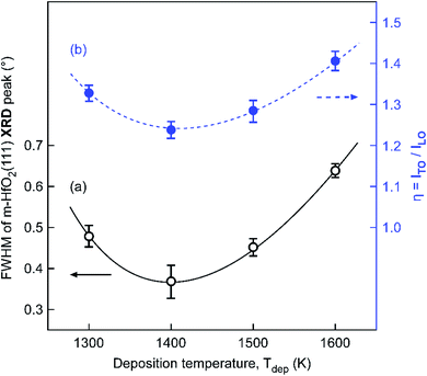 | ||
| Fig. 4 (a) FWHM of the m-HfO2 (111) XRD peak, and (b) intensity ratio η = ITO/ILO obtained from Raman spectra of the HfO2 film in the four regions, with Tdep ranging from 1300 K to 1600 K. | ||
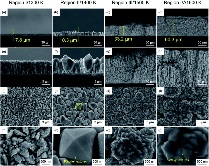
Fig. 5 shows SEM micrographs of the cross-section and surface of the HfO2 film in Regions I to IV as Tdep increased from 1300 K to 1600 K. Measurements taken from the cross-sectional SEM micrographs (Fig. 5(a)–(d)) show that the thickness increased from 7.8 μm to 60.3 μm, corresponding to calculated growth rates of 47–362 μm h−1. The surface SEM images show four morphologies in the as-deposited film. The cross-sectional micrographs show that the HfO2 film in Region I, formed at 1300 K, has a columnar microstructure. Aggregates of fine grains are arrayed in random lines on the film surface. The HfO2 film in Region II, formed at 1400 K, is composed of 〈002〉-oriented columnar grains, corresponding to μ-XRD patterns in Fig. 2(b). Fig. 5(n) shows a pyramidal faceted morphology of m-HfO2, with a parallel texture at the surface of 〈002〉-oriented m-HfO2 grains. Fig. S3(a)† shows the atomic nodes with a twofold rotational symmetry, which is the typical morphology of the P21/c space group. Javier Sanz et al. calculated the surface energies for the m-HfO2 (111) and (![[1 with combining macron]](https://www.rsc.org/images/entities/char_0031_0304.gif) 11) planes, lower than that for the (100) and (010) planes.36 The calculation was based on the Born–Oppenheimer molecular dynamics (BOMD) simulations. And lower surface energies usually correspond to exposed surfaces, as shown in Fig. S3(b).† The HfO2 film in Region III (1500 K) consists of crystal clusters. At the surface, the crystal clusters are aggregates of vertical bundles that are decorated allover with fine grains, presumably resulting from the coexistence of m- and t-HfO2. The HfO2 film in Region IV (1600 K) exhibits a cluster-like microstructure. The surface morphology in Region IV is similar to that in Region III, except that the grain size increases from ∼200 nm to ∼500 nm with increasing temperature, and a wavy texture observed at the surface in Region IV. The morphologies correspond to XRD patterns ranging from random (Region I) to highly oriented (Region II) and back to random (Regions III and IV) with increasing temperature.
11) planes, lower than that for the (100) and (010) planes.36 The calculation was based on the Born–Oppenheimer molecular dynamics (BOMD) simulations. And lower surface energies usually correspond to exposed surfaces, as shown in Fig. S3(b).† The HfO2 film in Region III (1500 K) consists of crystal clusters. At the surface, the crystal clusters are aggregates of vertical bundles that are decorated allover with fine grains, presumably resulting from the coexistence of m- and t-HfO2. The HfO2 film in Region IV (1600 K) exhibits a cluster-like microstructure. The surface morphology in Region IV is similar to that in Region III, except that the grain size increases from ∼200 nm to ∼500 nm with increasing temperature, and a wavy texture observed at the surface in Region IV. The morphologies correspond to XRD patterns ranging from random (Region I) to highly oriented (Region II) and back to random (Regions III and IV) with increasing temperature.
Fig. 6 shows a dependence of deposition rates (Rdep) on deposition temperatures (Tdep) of HfO2 films grown using HT-LCVD, with the presence of crystal phases (monoclinic, tetragonal or amorphous) and precursors, and the results are compared against those in the literature. In order to improve the measurement accuracy, the HfO2 film was divided into eight specimens, which were fabricated at 1250–1600 K using a single growth process. The Rdep of the HfO2 film prepared by HT-LCVD reached a maximum of 362 μm h−1 at Tdep = 1600 K, which was 102 to 104 times higher than that obtained using existing methods, such as MOCVD,8–12 TCVD,13 and ALD.14–18 Using the infrared temperature-measurement program, the microstructure of the HfO2 film was found to change from columnar to cluster-like at approximately 1420 K.
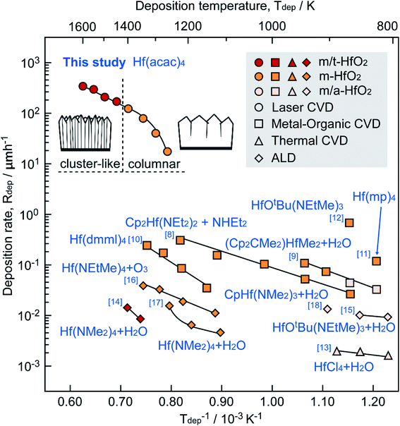 | ||
| Fig. 6 Effect of Tdep on Rdep and crystal phase of HfO2 films prepared using HT-LCVD, MOCVD, TCVD and ALD. | ||
The Arrhenius equation was used to calculate the activation energies (Ea)37 of the specimens as 100–220 kJ mol−1 in the curved regions over the range of 1250–1400 K (Regions I and II) and 80 kJ mol−1 in the linear part at Tdep = 1400–1600 K (Regions III and IV). The deposition rates in the curved regions were correlated with controlling kinetic mechanisms of deposition processes [i.e., the chemical reaction regime (CRR) or the mass transfer regime (MTR)], where the transition from CRR to MTR is normally induced by an increase in temperature.38,39 In Regions I and II, the slope of the Arrhenius equation decreased from 220 kJ mol−1 to 100 kJ mol−1, indicating a transition from the CRR to the MTR domain.
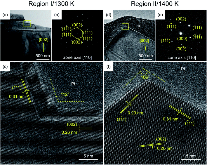
Fig. 7 shows the cross-section TEM images of specimens in Regions I and II. The bright-field (BF) image of the HfO2 film in Region I shows columnar grains with a variety of orientations. The selected area electron diffraction (SAED) pattern, which was exhibited in Fig. 7(b), was indexed to a set of well-defined (002) sites along the zone axis of [110]. Application of Vander Drift's evolutionary selection model38 to the high-resolution (HR) TEM image revealed exposed surfaces along the [![[1 with combining macron]](https://www.rsc.org/images/entities/char_0031_0304.gif) 11] or [002] directions, which explained why the fastest growing crystallographic plane overlaid the other growing planes. Nishioka et al.40 developed a model for the controlling mechanisms of the CVD processes by assuming Langmuir-type adsorption of the reactants. The HfO2 film in Region I, formed at 1300 K, was associated with the CRR, and Rdep was expressed as given in eqn (1):
11] or [002] directions, which explained why the fastest growing crystallographic plane overlaid the other growing planes. Nishioka et al.40 developed a model for the controlling mechanisms of the CVD processes by assuming Langmuir-type adsorption of the reactants. The HfO2 film in Region I, formed at 1300 K, was associated with the CRR, and Rdep was expressed as given in eqn (1):
| Rdep = krNhklV | (1) |
![[1 with combining macron]](https://www.rsc.org/images/entities/char_0031_0304.gif) 11] direction, in agreement with the XRD patterns. As there was insufficient energy for the system to reach the equilibrium state at a low temperature, supersaturation of m-HfO2 grains led to lattice distortion of the (
11] direction, in agreement with the XRD patterns. As there was insufficient energy for the system to reach the equilibrium state at a low temperature, supersaturation of m-HfO2 grains led to lattice distortion of the (![[1 with combining macron]](https://www.rsc.org/images/entities/char_0031_0304.gif) 11) planes and a variety of orientations in Region I. Fig. S4† shows three common growth models, named Frank–van der Merwe (2D), Volmer–Weber (3D), and Stranski–Krastanov (2D + 3D) models. The overall growth process of the HfO2 film in Region I could be considered an extension of the Stranski–Krastanov (SK) growth mode for a two-dimensional thin film to a finite 3D case, as shown in Fig. S4(c).†41
11) planes and a variety of orientations in Region I. Fig. S4† shows three common growth models, named Frank–van der Merwe (2D), Volmer–Weber (3D), and Stranski–Krastanov (2D + 3D) models. The overall growth process of the HfO2 film in Region I could be considered an extension of the Stranski–Krastanov (SK) growth mode for a two-dimensional thin film to a finite 3D case, as shown in Fig. S4(c).†41
The SAED in Fig. 7(e) for the HfO2 film in Region II is indexed to a set of (002) sites along the zone axis of [110]. The HRTEM image shows exposed surfaces corresponding to the (1![[1 with combining macron]](https://www.rsc.org/images/entities/char_0031_0304.gif) 1) and (
1) and (![[1 with combining macron]](https://www.rsc.org/images/entities/char_0031_0304.gif) 11) planes of m-HfO2. The HfO2 film in Region II, formed at 1400 K, was associated with the MTR, and Rdep was expressed using eqn (2):
11) planes of m-HfO2. The HfO2 film in Region II, formed at 1400 K, was associated with the MTR, and Rdep was expressed using eqn (2):
| Rdep = ksηhklV | (2) |
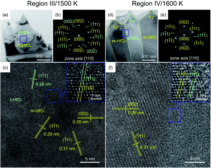
Fig. 8 shows the cross-section TEM images of specimens in Regions III and IV composed of monoclinic (yellow) and tetragonal (bright green) grains. When the deposition temperature exceeded 1500 K, the growth deviated from the equilibrium state again via the Volmer–Weber (VW) growth mode, and the increase in the concentration of activated molecules resulted in an increase in the supersaturation of the grains.38,42 The HRTEM images showed the in-plane boundary for m-HfO2(![[1 with combining macron]](https://www.rsc.org/images/entities/char_0031_0304.gif) 10) {111}//t-HfO2(1
10) {111}//t-HfO2(1![[1 with combining macron]](https://www.rsc.org/images/entities/char_0031_0304.gif) 1) {111}. The self-vanishing defects at the interface induced the migration of {111} planes, such that no distinct interface between the two phases of HfO2 could be observed.
1) {111}. The self-vanishing defects at the interface induced the migration of {111} planes, such that no distinct interface between the two phases of HfO2 could be observed.
Fig. S5† shows the dielectric measurements of the HfO2 films in different regions. The real parts of the complex permittivity of samples in four regions indicate the real-time storage capacity of the dielectric material to the applied high-frequency electric field. And the dielectric loss (tan![[thin space (1/6-em)]](https://www.rsc.org/images/entities/char_2009.gif) δ), the ratio of the imaginary-part to the real-part value, indicates the energy-loss degree in the use of dielectric materials. Fig. S5(d)† shows the curves of the real-part value of complex permittivity and dielectric loss in different regions. With the increase of Tdep, both of the permittivity and dielectric-loss values increase first and then decrease. In Region II (1400 K), the real-part value of complex permittivity reached the maximum value, 22, but the dielectric loss was also up to 0.60. When Tdep increased to 1500 K, the permittivity decreased slightly to 21, while the dielectric loss correspondingly decreased to 0.43. At 1600 K, the permittivity decreased to the minimum value,16 but still higher than that of traditional SiO2 layers (3.9).43
δ), the ratio of the imaginary-part to the real-part value, indicates the energy-loss degree in the use of dielectric materials. Fig. S5(d)† shows the curves of the real-part value of complex permittivity and dielectric loss in different regions. With the increase of Tdep, both of the permittivity and dielectric-loss values increase first and then decrease. In Region II (1400 K), the real-part value of complex permittivity reached the maximum value, 22, but the dielectric loss was also up to 0.60. When Tdep increased to 1500 K, the permittivity decreased slightly to 21, while the dielectric loss correspondingly decreased to 0.43. At 1600 K, the permittivity decreased to the minimum value,16 but still higher than that of traditional SiO2 layers (3.9).43
4. Conclusion
In this study, high-throughput HfO2 films were deposited on Si (100) substrates via HT-LCVD using Hf(acac)4 as a precursor. Two typical lattice stacking structures (SK and VW) were observed by TEM. The evolutions of microstructures and growth mechanisms of HfO2 films in different regions were studied by a continuous temperature field, which was controlled steadily with a large gradient (100 K mm−1). The HfO2 film obtained using a single growth process could be divided into four regions corresponding to increasing Tdep from 1300 K to 1600 K, with orientations ranging from random to highly oriented and back to random. The maximum deposition rate of 362 μm h−1 was 102 to 104 times higher than that obtained using existing CVD methods. The permittivity of the high-throughput HfO2 film is in the range of 16–22, and the permittivity reached the maximum value, 22, in Region II at 1400 K.Conflicts of interest
The authors declare that they have no conflict of interest.Acknowledgements
This work was supported by the National Natural Science Foundation of China (No. 51861145306, 51872212 and 51972244), and the 111 Project (B13035). It was also supported by the International Science & Technology Cooperation Program of China (2018YFE0103600), the Technological Innovation of Hubei Province, China (2019AAA030). It was also supported by the Key Area Research and Development Program of Guangdong Province (2019B121204001, 2020B010181001), the Chaozhou Science and Technology Project (2019PT01), the Self-innovation Research Funding Project of Hanjiang Laboratory (HJL202012A001, HJL202012A002, HJL202012A003) and the Major Science and Technology Project in Zhongshan City, Guangdong Province (2019AG029).References
- Y. Huang and C. Wan, J. Adv. Ceram., 2020, 9, 271–291 CrossRef CAS.
- L. Chen and J. Feng, J. Adv. Ceram., 2019, 8, 537–544 CrossRef CAS.
- J. H. Choi, Y. Mao and J. P. Chang, Mater. Sci. Eng., R, 2011, 72, 97–136 CrossRef.
- K. Matsumoto, Y. Itoh and T. Kameda, Sci. Technol. Adv. Mater., 2003, 4, 153–158 CrossRef CAS.
- I. K. Oh, J. Tanskanen, H. Jung, K. Kim, M. J. Lee, Z. Lee, S. K. Lee, J. H. Ahn, C. W. Lee, K. Kim, H. Kim and H. B. R. Lee, Chem. Mater., 2015, 27, 5868–5877 CrossRef CAS.
- J. C. Brewer, R. J. Walters, L. D. Bell, D. B. Farmer, R. G. Gordon and H. A. Atwater, Appl. Phys. Lett., 2004, 85, 4133–4135 CrossRef CAS.
- C. Zhang, F. Yun, J. L. Zhao, Y. Guang, H. F. Chen, L. M. Zhang, Y. F. Gao and B. Liu, J. Adv. Ceram., 2021, 10, 520–528 CrossRef CAS.
- G. Carta, N. El Habra, G. Rossetto, G. Torzo, L. Crociani, M. Natali, P. Zanella, G. Cavinato, V. Matterello, V. Rigato, S. Kaciulis and A. Mezzi, Chem. Vap. Deposition, 2007, 13, 626–632 CrossRef CAS.
- K. Black, H. C. Aspinall, A. C. Jones, K. Przybylak, J. Bacsa, P. R. Chalker, S. Taylor, C. Z. Zhao, S. D. Elliott, A. Zydor and P. N. Heys, J. Mater. Chem., 2008, 18, 4561–4571 RSC.
- T. J. Park, J. H. Kim, J. H. Jang, U. K. Kim, S. Y. Lee, J. Lee, H. S. Jung and C. S. Hwang, Chem. Mater., 2011, 23, 1654–1658 CrossRef CAS.
- T. S. Yang, K. S. An, E. J. Lee, W. Cho, H. S. Jang, S. K. Park, Y. K. Lee, T. M. Chung, C. G. Kim, S. Kim, J. H. Hwang, C. Lee, N. S. Lee and Y. Kim, Chem. Mater., 2005, 17, 6713–6718 CrossRef CAS.
- A. R. Teren, R. Thomas, J. He and P. Ehrhart, Thin Solid Films, 2005, 478, 206–217 CrossRef CAS.
- J. Chung, Y. J. Tak, W. G. Kim, J. W. Park, T. S. Kim, J. H. Lim and H. J. Kim, J. Mater. Chem. C, 2018, 6, 4928–4935 RSC.
- E. Jud, M. Tang and Y. M. Chiang, J. Appl. Phys., 2008, 103, 114108 CrossRef.
- M. Seo, Y. S. Min, S. K. Kim, T. J. Park, J. H. Kim, K. D. Na and C. S. Hwang, J. Mater. Chem., 2008, 18, 4324–4331 RSC.
- S. Y. Lee, H. K. Kim, J. H. Lee, I. H. Yu, J. H. Lee and C. S. Hwang, J. Mater. Chem. C, 2014, 2, 2558–2568 RSC.
- I. K. Oh, B. E. Park, S. Seo, B. C. Yeo, J. Tanskanen, H. B. R. Lee, W. H. Kim and H. Kim, J. Mater. Chem. C, 2018, 6, 7367–7376 RSC.
- S. Park, B. E. Park, H. Yoon, S. Lee, T. Nam, T. Cheon, S. H. Kim, H. Cheon, S. Im, T. Seong and H. Kim, J. Mater. Chem. C, 2020, 8, 1344–1352 RSC.
- O. Acton, G. Ting, H. Ma, J. W. Ka, H. L. Yip, N. M. Tucker and A. K. Y. Jen, Adv. Mater., 2008, 20, 3697–3701 CrossRef CAS.
- O. Acton, M. Dubey, T. Weidner, K. M. O'Malley, T. W. Kim, G. G. Ting, D. Hutchins, J. E. Baio, T. C. Lovejoy, A. H. Gage, D. G. Castner, H. Ma and A. K. Y. Jen, Adv. Funct. Mater., 2011, 21, 1476–1488 CrossRef CAS.
- M. B. Zakaria, T. Nagata and T. Chikyow, ACS Omega, 2019, 4, 14680–14687 CrossRef CAS.
- E. Verrelli and D. Tsoukalas, J. Appl. Phys., 2013, 113, 114103 CrossRef.
- Y. Wang, H. Wang, C. Ye, J. Zhang, H. Wang and Y. Jiang, ACS Appl. Mater. Interfaces, 2011, 3, 3813–3818 CrossRef CAS PubMed.
- S. Zhang, R. Tu, T. Goto and W. Petuskey, J. Am. Ceram. Soc., 2012, 95, 2782–2784 CrossRef CAS.
- S. Zhang, Q. Xu, R. Tu, T. Goto, L. Zhang and T. Besmann, J. Am. Ceram. Soc., 2014, 97, 952–958 CrossRef CAS.
- S. Yu, R. Tu and T. Goto, J. Eur. Ceram. Soc., 2016, 36, 403–409 CrossRef CAS.
- Y. You, A. Ito, R. Tu and T. Goto, Surf. Coat. Technol., 2013, 232, 1–5 CrossRef CAS.
- C. Chi, H. Katsui, R. Tu and T. Goto, Mater. Chem. Phys., 2014, 143, 1338–1343 CrossRef CAS.
- D. Guo, Y. Ju, A. Ito, T. Goto, C. Wang, Q. Shen, R. Tu, Z. Huang and L. Zhang, Ceram. Int., 2016, 42, 11464–11467 CrossRef CAS.
- T. Wang, K. Wang, R. Tu, S. Zhang, M. Yang, Q. Li, J. Shi, H. Li, T. Goto and L. Zhang, RSC Adv., 2017, 7, 56166–56172 RSC.
- S. Zhang, Q. Xu, R. Tu, T. Goto, L. Zhang and G. Brennecka, J. Am. Ceram. Soc., 2015, 98, 236–241 CrossRef CAS.
- P. J. McGinn, ACS Comb. Sci., 2019, 21, 501–515 CrossRef CAS PubMed.
- Q. Xu, R. Tu, Q. Sun, M. Yang, Q. Li, S. Zhang, L. Zhang, T. Goto, H. Ohmori, J. Shi, H. Li, M. Kosinova and B. Bikramjit, RSC Adv., 2019, 9, 2426–2430 RSC.
- T. Torchynska, L. G. V. Macotela, L. Khomenkova and F. Gourbilleau, J. Electron. Mater., 2020, 49, 3441–3449 CrossRef CAS.
- S. N. Tkachev, M. H. Manghnani, A. Niilisk, J. Aarik and H. Mandar, J. Mater. Sci., 2005, 40, 4293–4298 CrossRef CAS.
- A. B. Mukhopadhyay, C. B. Musgrave and J. F. Sanz, J. Am. Chem. Soc., 2008, 130, 11996–12006 CrossRef CAS.
- K. Xu, A. P. Milanov, M. Winter, D. Barreca, A. Gasparotto, H. W. Becker and A. Devi, Eur. J. Inorg. Chem., 2010, 11, 1679–1688 CrossRef.
- R. Tu, D. Zheng, Q. Sun, M. Han, S. Zhang, Z. Hu, T. Goto, L. Zhang and T. Besmann, J. Am. Ceram. Soc., 2016, 99, 84–88 CrossRef CAS.
- F. Loumagne, F. Langlais, R. Naslain, S. Schamm, D. Dorignac and J. Sévely, Thin Solid Films, 1995, 254, 75–82 CrossRef CAS.
- K. Nishioka, N. Mizutani and H. Komiyama, J. Electrochem. Soc., 2000, 147, 1440–1442 CrossRef CAS.
- M. H. Oh, M. G. Cho, D. Y. Chung, I. Park, Y. P. Kwon, C. Ophus, D. Kim, M. G. Kim, B. Jeong, X. W. Gu, J. Jo, J. M. Yoo, J. Hong, S. McMains, K. Kang, Y. E. Sung, A. P. Alivisatos and T. Hyeon, Nature, 2020, 577, 359–363 CrossRef CAS.
- B. J. Kooi and M. Wuttig, Adv. Mater., 2020, 32, 1908302 CrossRef CAS PubMed.
- K. Nakamura, K. Doi, K. Fujitani and A. Tachibana, Phys. Rev. B: Condens. Matter Mater. Phys., 2005, 71, 045332 CrossRef.
Footnote |
| † Electronic supplementary information (ESI) available. See https://doi.org/10.1039/d2ra01573k |
| This journal is © The Royal Society of Chemistry 2022 |

