
 Open Access Article
 This Open Access Article is licensed under a Creative Commons Attribution-Non Commercial 3.0 Unported Licence
Electronic structure, magnetoresistance and spin filtering in graphene|2 monolayer-CrI33|graphene van der Waals magnetic tunnel junctions†
Yibin Zhang‡
a,
Jie Liu‡ a,
Renhao Denga,
Xuan Shi*bc,
Huan Tanga,
Hong Chena and
Hongkuan Yuan*ad
a,
Renhao Denga,
Xuan Shi*bc,
Huan Tanga,
Hong Chena and
Hongkuan Yuan*ad
aSchool of Physical Science and Technology, Southwest University, Chongqing, 400715, China. E-mail: yhk10@swu.edu.cn
bCenter of Quantum Information Technology, Chongqing Institute of Green and Intelligent Technology, Chinese Academy of Sciences, Chongqing, 400714, China. E-mail: shixuan@cigit.ac.cn
cCollege of Artificial Intelligence, Chongqing School, University of Chinese Academy of Sciences, Chongqing, 400714, China
dChongqing Key Laboratory of Micro&Nano Structure Optoelectronics, Chongqing, 400715, China
First published on 6th October 2022
Abstract
In the pursuit of designing van der Waals magnetic tunneling junctions (vdW-MTJs) with two-dimensional (2D) intrinsic magnets, as well as to quantitatively reveal the microscopic nature governing the vertical tunneling pathways beyond the phenomenological descriptions on CrI3-based vdW-MTJs, we investigate the structural configuration, electronic structure and spin-polarized quantum transport of graphene|2 monolayer(2ML)-CrI3|graphene heterostructure with Ag(111) layers as the electrode, using density functional theory (DFT) and its combination of non-equilibrium Green’s function (DFT-NEGF) methods. The in-plane lattice of CrI3 layers is found to be stretched when placed on the graphene (Gr) layer, and the layer-stacking does not show any site selectivity. The charge transfer between CrI3 and Gr layers make the CrI3 layer lightly electron-doped, and the Gr layer hole-doped. Excitingly, the inter-layer hybridization between graphene and CrI3 layers render the CrI3 layer metallic in the majority spin channel, giving rise to an insulator-to-half-metal transition. Due to the metallic/insulator characteristics of the spin-majority/minority channel of the 2ML-CrI3 barrier in vdW-MTJs, Gr|2ML-CrI3|Gr heterostructures exhibit an almost perfect spin filtering effect (SFE) near the zero bias in parallel magnetization, a giant tunneling magnetoresistance (TMR) ratio up to 2 × 10⁴%, and remarkable negative differential resistance (NDR). Our results not only give an explanation for the observed giant TMR in CrI3-based MTJs but also show the direct implications of 2D magnets in vdW-heterostructures.
I. Introduction
Vertical stacking of distinctive two-dimensional (2D) magnetic van der Waals (vdW) layers enables the creation of diverse vdW heterostructures, which open a new avenue for the development of novel spintronic and magnonic devices such as magnetic tunneling junction (MTJ), spin-filtering MTJ, spin valve, spin tunnel field-effect transistors and spin logic circuit.1–6 Among these spin-dependent devices, vdW-MTJ as a highly desirable building block for state-of-the-art spintronic devices, has attracted significant interest because the integration of distinctive 2D vdW-layers without chemical bonds can provide promising solutions to the adverse effects of processing technology, e.g., defect/disorder in the electrodes and barrier, interface diffusion and poor thermal stability that lead to low tunnel magnetoresistance (TMR).1,2 Unlike conventional multilayer MTJ devices where two ferromagnetic layers are separated by a nonmagnetic insulator layer, ferromagnetic vdW-monolayers can serve simultaneously as the tunneling barrier and TMR-related free ferromagnetic layer in vdW-MTJs.7–10 This functional combination enables spintronic devices to be ultracompact and to be modulated efficiently by electrical means. Their uniform thickness barrier layers should facilitate the all-area tunneling; the sharp atomic interface between spin filters can guarantee the achievement of large TMR. Consequently, a research field around vdW-MTJs has emerged and has been gaining strength over the past two years.1–6Inspired by the recent discovery of 2D-vdW ferromagnetic materials of CrI3,11 Cr2Ge2Te6,12 VSe2 (ref. 13) and Fe3GeTe2 (FGT),14,15 together with the fascinating observation of large TMR in CrI3-based vdW-MTJs,7–10 numerous vdW-MTJs have been artificially designed and successfully fabricated. These research articles focused on vdW-MTJs with the aforementioned 2D magnets, including Gr|CrI3|Gr,16–20 Gr|CrBr3|Gr,21 CrI3|h-BN|CrI3,22 Cu|CrI3|Cu,23 Cu|CrI3|h-BN|CrI3|Cu,24 VSe2|CrI3|VSe2,25 CrI3|Li0.5CrI3|CrI3,26 FGT|h-BN|FGT,27,28 FGT|InSe|FGT,29 FGT|MoS2|FGT,30 MoSe2|VSe2|WSe2|VSe2|MoSe2,31 VSe2|MoS2|VSe2,32 CrTe2|Gr|CrTe2 or CrTe2|h-BN|CrTe2,33 and so on. The graphite|nML-CrI3|graphite vertical MTJ is the most attractive prototype, because its maximal TMR were experimentally reported to be 0.55 × 10³%,7 1.9 × 10⁴%,8 1 × 10⁴%,9 and 1 × 10⁶%,10 respectively. With the increase of anti-aligned spin filters in MTJs by increasing the CrI3 barrier from bilayer, trilayer to tetralayer, Klein et al.7 have measured a remarkable increase in TMRs of 95, 300, 550%, respectively; while Song et al.8 have observed the highest values of 530, 3200, 19![[thin space (1/6-em)]](https://www.rsc.org/images/entities/char_2009.gif) 000%, respectively. Generally, CrI3-based vdW-MTJs exhibit thickness-dependent transports with desirable performance such as a large TMR; the transport mechanism can be qualitatively understood in terms of multi-layer spin-filtering effects.8 Nevertheless, as clearly pointed out by Klein et al.,7 the transport calculations on CrI3-based vdW-MTJs should be done to elucidate their precise tunneling pathways by inspecting the electronic structures.
000%, respectively. Generally, CrI3-based vdW-MTJs exhibit thickness-dependent transports with desirable performance such as a large TMR; the transport mechanism can be qualitatively understood in terms of multi-layer spin-filtering effects.8 Nevertheless, as clearly pointed out by Klein et al.,7 the transport calculations on CrI3-based vdW-MTJs should be done to elucidate their precise tunneling pathways by inspecting the electronic structures.
From the computational aspect on CrI3-based MTJs, DFT-NEGF transport calculations have been performed on the heterojunctions within a few monolayers (MLs), i.e., 1ML-CrI3 barrier sandwiched between graphite electrodes,19 3ML-CrI3 barrier sandwiched between graphite electrodes,20 4ML-CrI3 barrier sandwiched between Cu(111) electrodes.23 By taking hexagonal boron nitride (h-BN) as the tunneling barrier and CrI3 layers as the ferromagnetic layer, 1ML-CrI3|h-BN|nML-CrI3 heterojunctions sandwiched between noble-metal (Cu, Ag, Au) electrodes have been investigated.22,24 In the above MTJ models with metal as the electrode, metal layers were directly contacted with CrI3 layers, which leads to an important feature in electronic structure that is different from the expected one. Furthermore, from the point of view of device fabrication, the contact between metal electrodes and heterostructure material is often realized by the molecular beam epitaxy (MBE) method. If CrI3 magnetic layers are not protected by graphene, lattice mismatch and chemical bonding with metal atoms during the MBE fabrication would lead to diffusion/disorder/defect and conductivity mismatch at the metal|CrI3 interfaces, which may result in low spin injection in a realistic scenario.1,2 To solve the problem of MTJ fabrication, it is necessary to interpolate a Gr layer between metal lead and CrI3 layers.2
The theoretical MTJ models with graphite as the electrode are different from the experimentally fabricated device structures where the top/bottom few-layer Gr flakes were in contact with the pre-patterned metal electrodes,7–10,16,17 i.e., few-layer Gr were incorporated in CrI3-based MTJ. In previously theoretical work, the lattice constants of Gr layers were strained or compressed to match with the CrI3 layers,19,20 which would significantly influence the TMR and conductance of MTJ via the variation of the band-gap of Gr layers.19 In this work, the lattice constants of CrI3 layers were strained or compressed to match with Gr layers regarding the large Young’s modulus of Gr layer. So far, essentially no theoretical work has been done to investigate the electronic structures and transport properties of Gr|2ML-CrI3|Gr devices with metal electrodes. It remains to be determined whether the interpolation of Gr layers causes new interesting physical phenomena to appear. This is expected because in CrI3|2ML-Gr|CrI3 vdW-type spin valves,34 the band structures of the Gr layer were preserved in the minority spin channel while strong hybridizations at the CrI3|Gr interface open up a Dirac gap in the majority spin channel.
In this paper, we combine DFT method and quantum ballistic DFT-NEGF transport calculations on Gr|2ML-CrI3|Gr vdW-MTJ to study interface configurations and electronic structures as well as to reveal the microscopic nature governing the spin-dependent transport properties. This device model consists of face-centered cubic (fcc) Ag(111) electrodes, interpolation Gr monolayer, and magnetic 2ML-CrI3 barrier layers. Our results reveal that Gr and CrI3 layers can be stably bonded together through the weak vdW-interaction. The hybridizations between them make 2ML-CrI3 layers exhibit a half-metallic feature and open a small Dirac-gap in the spin-majority channel for Gr layers. The perfect spin filter effects provided by 2ML-CrI3 layers, in addition to graphene barrier layers, lead to Gr|2ML-CrI3|Gr to show a giant TMR ratio reaching up to 2 × 10⁴%. We illustrate the mechanism of quantum transport from two aspects of precise tunneling pathways and electronic structures and give consistent interpretations.
II. Computational methods
The calculations for the structure relaxation, different interfaces, electronic structure and magnetism are performed within the framework of spin-polarized density functional theory (DFT) implemented in Vienna ab initio Simulation Package (VASP).35–38 We adopt the exchange and correlation function with the Perdew–Burke–Ernzerhof (PBE) parameterization to describe the generalized gradient approximation (GGA).39,40 The valence electrons of C (2s22p2), Cr (3d54s1) and I (5s25p5) atoms are explicitly treated by the plane wave method, and the interactions of valence electrons with ionic cores are described by projected augmented plane wave (PAW) pseudopotentials,41,42 where the plane-wave cutoff energy is set to 400 eV. For structural optimization and electronic structure analyses, the gamma (G)-centered Monkhorst–Pack k-point grids of 6 × 6 × 1 and 12 × 12 × 1 are employed, respectively. We use the Grimme (DFT-D2) functional to include the vdW interaction.43 For transition metal (TM) atoms, the electron correlation effect is important due to the certain localization of their d electrons.44 Thus, the on-site Coulomb interaction U and exchange interaction J45,46 are set to be 3.2 eV and 0.7 eV, respectively, and the effective value Ueff = 3.2 − 0.7 = 2.5 eV as reported in the literature.47 Spin–orbit coupling (SOC) interactions, known to be important to determine the magnetic anisotropy, are included in the calculation of magnetic moment and magnetic anisotropy energy (MAE). Lattice constants and atomic coordinates are fully relaxed with the criterion 10−6 eV for the self-consistent field (SCF) procedure, and the maximum residual force on each atom is less than 0.001 eV Å−1.
The unit cell of the CrI3 layer in the hexagonal 2D structure has the experimental lattice constant of a = b = 6.867 Å.48 To make a compromised computational performance between efficiency and precision, the Gr|2ML-CrI3|Gr heterostructure is built by depositing a (5 × 5) supercell of Gr layer (a = 12.295 Å) on both sides of a  supercell of CrI3 bilayer (a = 11.977 Å), as illustrated in Fig. 1. To obtain the optimal vdW gap and gain the favorable interface between the Gr layer and CrI3 layer, firstly, we individually relax the Gr|CrI3 bilayer and 2ML-CrI3 bilayer to extract their minimum-energy distances. Then, the sandwich-like Gr|2ML-CrI3|Gr heterostructure is designed by fixing these optimal distances and favorable interfaces. There are 100 C atoms, 36 I atoms and 12 Cr atoms in the heterostructure. The lattice mismatch between graphene and CrI3 layers is less than 3%, suggesting the possibility of good epitaxy. To avoid the imaging interaction, we add a vacuum region of 15 Å vacuum space layer on both sides of the graphene layers.
 | ||
| Fig. 1 Schematic sketch of the Gr|2ML-CrI3(AB)|Gr MTJ. The red dashed rectangle represents the central scattering region. The z-axis is the transport direction. | ||
To study the quantum transport properties of the Gr|2ML-CrI3|Gr heterostructure, Ag(111) layers as the electrodes are added on both sides of the heterostructure to build a device model. Although (4 × 4) Ag(111) layers are better to directly add on both sides of the heterostructure (lattice mismatch about 6%), there are too many atoms in this structure and the following computational costs are too expensive. A compromising choice with respect to both accuracy and efficiency is to place (3 × 3) graphene on both sides of the (1 × 1) 2ML-CrI3 layers, followed by adding  Ag(111) layers, where the lattice constant was fixed to the value of the 2ML-CrI3 layer. About 9% expansion of the lattice constant of Ag(111) layers is reasonable because the metallic characteristic of Ag(111) layers changes little with the variation of lattice constant. More importantly, by analyzing the band structures of the Gr|2ML-CrI3|Gr heterostructure in the (5 × 5)Gr|
 2ML-CrI3|(5 × 5)Gr structure and the realistic space density of states of the (3 × 3)Gr|(1 × 1)2ML-CrI3|(3 × 3)Gr device structure (Fig. 9), we obtain good consistent transport results. This suggests that the electronic structures of the Gr|2ML-CrI3|Gr heterostructure are maintained in the device structure. This two-probe MTJ device model can be divided into three regions: left semi-infinite Ag(111) electrode, central scattering region 4ML-Ag|Gr|2ML-CrI3|Gr|4ML-Ag, and right semi-infinite Ag(111) electrode. The 4ML-Ag(111) layers of the scattering region are the buffer layers to shield the Hartree potential and identify the boundary conditions; two Ag electrodes can extend to z = ±∞ (transport direction). Our proposed structure is like a spin-filter MTJ, where magnetic 2ML-CrI3 insulators act as a tunneling barrier for vertical transport.7–10 The calculations of spin-dependent transport properties are performed using state-of-the-art techniques, i.e., the combination of DFT with the NEGF method implemented in Nanodcal package.49–51 Here, we use a linear combination of atomic orbital basis sets with double-zeta plus polarization basis,53,54 SCF criteria of 10−5 eV, cut-off energy of 100 Hartree, G-centered Monkhorst–Pack k-points of 6 × 6 × 1 and 40 × 40 × 1 for density matrix convergence and transmission coefficients, respectively. The spin resolved transmission Ts(E) across the tunnel junction at equilibrium is calculated via the formula of Ts(E) = Tr[ΓLGRΓRGA], where s denotes the spin-up or spin-down conduction channels, ΓL/ΓR is the coupling matrix of the left/right electrode, GR/GA is the retarded/advanced Green’s functions of the center region. The spin-dependent current is calculated by the Landauer–Büttiker formula:52
  where σ ≡ ↑, ↓ means the spin index; μL (μR) and fL (fR) are the electrochemical potential and the Fermi distribution function of the left (right) electrode, respectively; VL/R are the bias voltages applied on the electrodes. The total current is defined by I = I↑ + I↓.
III. Results and discussion
A. Structures and stability
![[3 with combining macron]](https://www.rsc.org/images/entities/char_0033_0304.gif) bulk of CrI3, we obtained their in-plane lattice constants of a = b = 6.915 Å, 6.913 Å and 6.909 Å, respectively. Compared with the experimental value of 6.867 Å,48 we found that our PBE+U+D2 values are better than the previous PBE value of 7.00 Å,55,56 PBE+U value of 7.08 Å,57 suggesting the importance of the vdW-interaction. We have performed the HSE06 calculation as well as the PBE+U calculation without the D2-type vdW correction, and found that the CrI3 monolayer has lattice constants of 6.899 Å and 7.071 Å, respectively. Note that the small change in lattice constants have a slight effect on the electronic structure of the CrI3 layer.58 It is well known that the CrI3 layer has a semiconducting band gap and the single Gr layer is a semi-metal with a zero gap. Our calculated band structures and the partial densities of states of CrI3 and Gr monolayers are shown in Fig. S1 and S2 (ESI).† The CrI3 layer has a calculated band gap of 0.97 eV, which is consistent with the previous PBE+U value of 1.05 eV (ref. 57) but is smaller than the measured value of 1.2 eV (ref. 59) due to the intrinsic deficiency of the standard DFT approach.60 Typically, the conduction band minimum (CBM) is far from the Fermi level but the valence band maximum (VBM) is close to the Fermi level, both of which are contributed by the majority spin states (Fig. S1 in ESI†). For the Gr layer, its semi-metal character is well preserved owing to the perfect Dirac cone at the Fermi level (Fig. S2 in ESI†).
bulk of CrI3, we obtained their in-plane lattice constants of a = b = 6.915 Å, 6.913 Å and 6.909 Å, respectively. Compared with the experimental value of 6.867 Å,48 we found that our PBE+U+D2 values are better than the previous PBE value of 7.00 Å,55,56 PBE+U value of 7.08 Å,57 suggesting the importance of the vdW-interaction. We have performed the HSE06 calculation as well as the PBE+U calculation without the D2-type vdW correction, and found that the CrI3 monolayer has lattice constants of 6.899 Å and 7.071 Å, respectively. Note that the small change in lattice constants have a slight effect on the electronic structure of the CrI3 layer.58 It is well known that the CrI3 layer has a semiconducting band gap and the single Gr layer is a semi-metal with a zero gap. Our calculated band structures and the partial densities of states of CrI3 and Gr monolayers are shown in Fig. S1 and S2 (ESI).† The CrI3 layer has a calculated band gap of 0.97 eV, which is consistent with the previous PBE+U value of 1.05 eV (ref. 57) but is smaller than the measured value of 1.2 eV (ref. 59) due to the intrinsic deficiency of the standard DFT approach.60 Typically, the conduction band minimum (CBM) is far from the Fermi level but the valence band maximum (VBM) is close to the Fermi level, both of which are contributed by the majority spin states (Fig. S1 in ESI†). For the Gr layer, its semi-metal character is well preserved owing to the perfect Dirac cone at the Fermi level (Fig. S2 in ESI†).For the CrI3 bilayer in AB-stacking (Fig. 2a), the intra-layer Cr–Cr distance of 3.989 Å and the inter-layer spacing of 6.581 Å are consistent with the experimental values of 3.965 Å and 6.602 Å,48 respectively, and also comparable to previously theoretical values of 3.98–4.06 Å and 6.68–6.78 Å,61 respectively. It is found that the inter-layer ferromagnetic ordering is 18 meV more stable than anti-ferromagnetic ordering, which is in line with the previously reported 13 meV.61,62 Although a recent experiment has reported the antiferromagnetic order of CrI3 bilayer by exfoliating it from the CrI3 bulk,11 it is still uncertain whether the experimentally exfoliated CrI3 bilayer is AB-stacking or AB′-stacking because AB-stacking in a monoclinic phase structure favors the interlayer ferromagnetic order but AB′-stacking in rhombohedral phase structure favors the interlayer antiferromagnetic order.61–63 The magnetic ground state strongly relies on the initial geometry of the bilayer. For the CrI3 bilayer in AB′-stacking pattern (Fig. 2b), its lattice constant as well as the band structures are analogous to those of AB-stacking. The AB-stacking is 21 meV and 3 meV more stable than AB′-stacking in ferromagnetic and ferromagnetic orders, respectively. Thus, the CrI3 bilayer in AB-stacking has been used to calculate the following structural stability, electronic structures and transport properties of the different heterostructures.
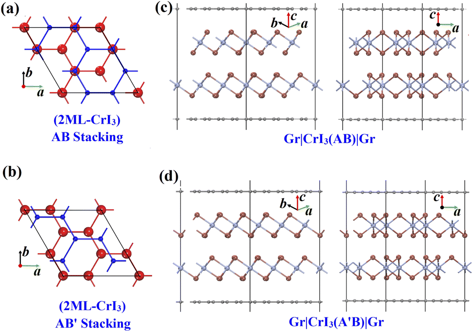 | ||
| Fig. 2 Frame structures of AB (a) and AB′ (b) stacking CrI3 bilayers are represented by hexagonally connected Cr atoms (red: bottom layer; blue: top layer). Stacking configurations of Gr|2ML-CrI3(AB)|Gr (c) and Gr|2ML-CrI3(AB′)|Gr (d) heterostructures. | ||
 , we found that the vdW-gap (distance between Gr and CrI3 layers) are in a very narrow range of 3.548–3.562 Å for various stacking, and the energy differences between the lowest and highest are less than 0.2 meV per C atom. The equilibrium vdW-gaps using our GGA+U+D2 method are generally in agreement with previous values of 3.53 Å using the GGA+D2 method and 3.57 Å using the GGA+optB86b method.58
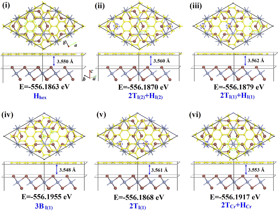 | ||
| Fig. 3 Six representative interfaces between Gr and CrI3 layers in Gr|CrI3 heterostructures, where yellow, brown and blue balls denote the C, I and Cr atoms, respectively. Total energy and representative indexes are below each configuration. (i) Hhex: a hexagonal C-ring in CrI3 hollow sites; (ii) 2TI(2) + HI(2): two C atoms and one hexagonal C-ring on top of I atoms of the bottom I(2) layer; (iii) 2TI(1) + HI(1): similar to (ii) but on top I atoms of top I(1) layer; (iv) 3BI(1): three C atoms bridged with its neighboring top I(1) atoms; (v) 2TI(1): two C atoms on top I(1) atoms; (vi) 2TCr + HCr: similar to (ii) but on Cr atoms. | ||
By calculating the interaction energy Einter, between Gr and CrI3 layers, via Einter = (ECrI3 + EGr − EHeter)/nC, we obtained Einter = 38.415 meV for the 3BI(1) interface configuration, which is comparable to the values found in other vdW systems. Here, total energies E are for the isolated CrI3 monolayer, Gr monolayer and Gr|CrI3 heterostructure with the same in-plane lattice of 7.00 Å, respectively, and nC is the number of C atoms. A small Einter demonstrates the weak vdW interaction between the Gr layer and CrI3 layer. Due to small fluctuating magnitudes in inter-layer interaction (2 meV/38.415 meV = 5%) and the vdW-gap (0.014 Å/3.562 Å = 0.4%), we can reasonably deduce that the stability of the Gr|CrI3 heterostructure is almost independent of stacking types, and the Gr layer can be placed on the CrI3 layer without any site selectivity.58 Therefore, it is advantageous in the process of stacking Gr|2ML-CrI3|Gr heterostructure with disregard for possible CrI3|Gr interfaces.
 corresponds to the experimental lattice constant of the CrI3 unit cell.48 The positive and negative ε represent the tensile and compressive strain on CrI3 layers, respectively. From Fig. 4b, we found that FM ordering is always more favorable than AFM ordering for AB stacking; from Fig. 4c, the heterostructure possesses the lowest total energy when the lattice constant is nearly equal to the value of the isolated Gr layer (2.459 × 5 = 12.295 Å; C–C bond-length 1.420 Å). This corresponds to ε = 3.37% lattice stretching of the CrI3 monolayer and suggests that the CrI3 layer will suffer larger lattice deformation than the Gr layer. In fact, the Young’s modulus of the CrI3 monolayer (28 N m−2) is significantly lower than that of the Gr monolayer (340 N m−2).64,65 Therefore, the lattice constants and thus the electronic structure of the Gr layer will essentially not be affected in a heterostructure, and the lattice mismatch only provides changing lattice constants and the tuning of magnetic states of CrI3 layers. Although available experiments have not explicitly indicated the lattice matching information when combined together,7–10 our findings question the rationality of previous work where MTJ structures were designed by straining or compressing the lattice constants of Gr layers to match with the CrI3 layers.19,20
 | ||
Fig. 4 (a) Schematic structure of Gr|2ML-CrI2(AB)|Gr heterostructure. Inter-layer distances are represented by different dn; (b) energy differences between ferromagnetic and anti-ferromagnetic ordering; (c) relative energy with respect to equilibrium structure, 2ML-CrI3 inter-layer distance d3 (inset); (d) inter-layer distance d5 between top and bottom-Gr layers (d4 between top and bottom-Cr layers); (e) thickness of top/bottom CrI3 layer  ; (f) vdW-gap ; (f) vdW-gap  between Gr and its nearest I layers as a function of biaxial strain ε = (a − a0)/a0 × 100% for AB stacking of the CrI3 bilayer. The ε = 0 corresponds to experimental lattice constant of the pristine CrI3 layer (a0 = 6.867 Å); the lowest energy structure (red symbols) correspond to the stretched lattice constant of the CrI3 layer (a = 7.099 Å; ε = 3.34%) and is equal to the lattice constant of the pristine Gr layer (a0 = 2.459 Å). between Gr and its nearest I layers as a function of biaxial strain ε = (a − a0)/a0 × 100% for AB stacking of the CrI3 bilayer. The ε = 0 corresponds to experimental lattice constant of the pristine CrI3 layer (a0 = 6.867 Å); the lowest energy structure (red symbols) correspond to the stretched lattice constant of the CrI3 layer (a = 7.099 Å; ε = 3.34%) and is equal to the lattice constant of the pristine Gr layer (a0 = 2.459 Å). | ||
In Fig. 4c–f, we plotted the various interlayer distances (vdW-gaps) as a function of lattice variations for heterostructure with AB stacking consequence in the FM state. With the increase of the in-plane lattice, the interlayer distance between two CrI3 monolayers (d3: inset in Fig. 4c) and the thickness of heterostructure (d5: Fig. 4d) remain nearly constant, while the thicknesses of the CrI3 monolayer (d2 and  ; Fig. 4e) decrease monotonously, resulting in a gradual increase of Gr–CrI3 distance (vdW-gaps d1 and
  ; Fig. 4f). These variations demonstrate that the vdW interaction is stronger between CrI3 bilayers than between Gr and CrI3 layers. The resultant layer spacing d4 = 6.52 Å (between CrI3 layers) as well as the layer separation d1 = 3.58 Å (between adjacent CrI3 and Gr layers) are in good agreement with the corresponding values of other studies.20,23,48,58
B. Electronic structure of Gr|2ML-CrI3(AB)|Gr
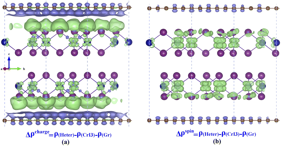 | ||
| Fig. 5 (a) Charge density difference and (b) spin density difference (isosurface value: 0.0015 e Å−3) of Gr|2ML-CrI3|Gr from side-view. Green and blue colors denote the accumulation and depletion of density area, respectively. | ||
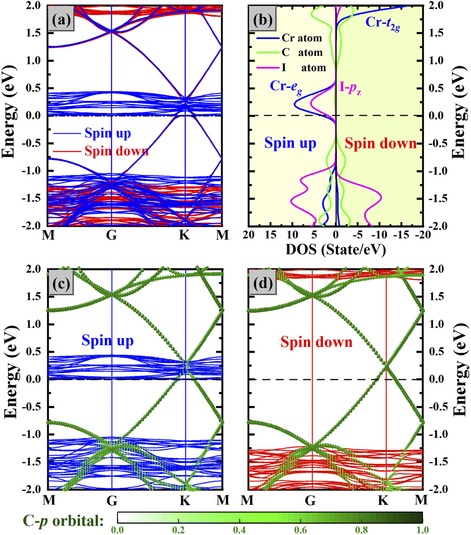 | ||
| Fig. 6 (a) Band structure of Gr|2ML-CrI3(AB)|Gr with FM alignment between 2ML-CrI3 layers. Blue and red lines represent spin-up and spin-down channels, respectively; (b) partial density of states (PDOS) resolved to elemental atoms; (c and d) projected band structures of C atoms for spin-up and spin-down channels (green balls). The contribution weight of the p-orbital to each band is represented by the depth of green color (ball color). | ||
From Fig. 6c for the spin-majority band (blue lines), Cr-eg and I-pz states of the CrI3 bilayer are strongly hybridized with the Gr-Dirac-cones, which opens up 0.2 eV Dirac-gap in a spurious manner (small but nonzero contribution weight). Although there is the Dirac-gap of two side Gr layers, the dispersions of some occupied Dirac states would contribute to the conductance to a degree, and this low barrier can be easily crossed when a small bias voltage is applied. Consequently, the crossing of band structure of 2ML-CrI3 layers around the Ef in the spin-majority band indicates that the spin-up electrons can transfer from the top Gr layer to 2ML-CrI3 layer and then through the bottom Gr layer.
In the spin-minority band (Fig. 6d), the Gr-Dirac-cones are basically unaffected and maintain the intactness, and the band structures of 2ML-CrI3 layers present the wide-gap semiconducting feature (3.0 eV; red lines). Note that the Ef level does not lie at the Dirac-point of Gr due to the dipolar field between Gr and CrI3 layers. Although the spin-down electrons could pass through the top Gr layer owing to its metallic feature, they will be blocked by the high barrier of the semiconducting 2ML-CrI3 layers. Therefore, the metallic/semiconducting characteristics of the spin-majority/minority channel of CrI3 bilayer in FM alignment lead to the result that the spin-up electrons can move vertically through the different layers but the spin-down electrons cannot. On the whole, the hybridization at the CrI3|Gr interface lowers the conduction band minimum (CBM) of the CrI3 layers in the spin majority channel while the spin minority band structures remain nearly unchanged, which determines the height of spin-dependent tunneling barriers and controls the transport properties.
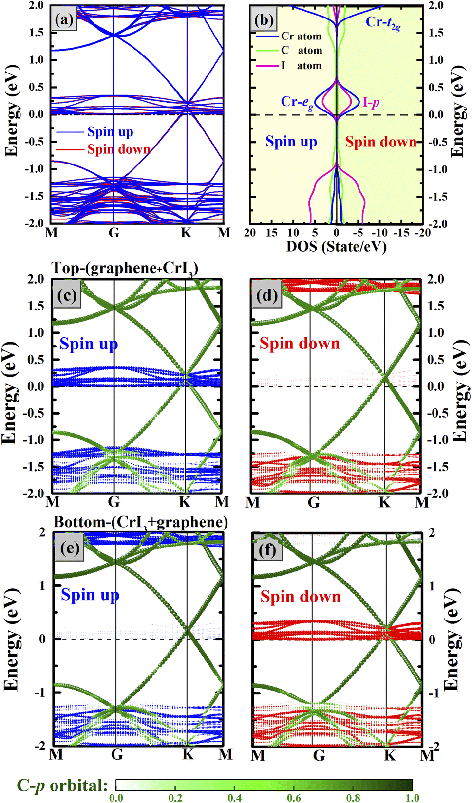 | ||
| Fig. 7 (a and b) are the same as in Fig. 6 but for AFM alignment. (c) and (d) are the spin-majority and spin-minority channels for the upper-half of the heterostructure; (e and f) for the lower-half of the heterostructure. The contribution to each band is divided from the CrI3 layer (blue/red balls) and Gr layer (green balls), respectively. | ||
C. Transport properties of Ag|Gr|2ML-CrI3|Gr|Ag
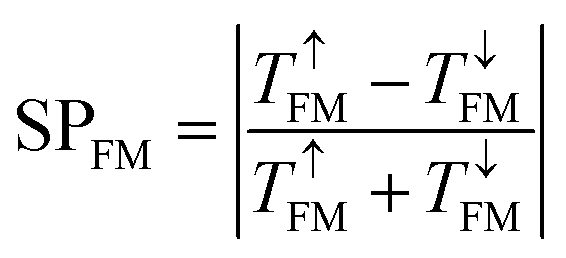 , is virtually 100%, verifying the perfect SFE in FM state. This evidence is explained by the band structure analyses shown in Fig. 6. For 2ML-CrI3 layers in AFM alignment, the curves of the spin-up and spin-down transmission coefficients nearly coincide with each other because of the mirror-symmetry of band structure shown in Fig. 7. Although there is a large peak at E = 0.06 eV, it is 2 orders of magnitude smaller than that of FM alignment, not to mention the fact that it’s energy position is far away from the Ef. By amplifying the curves around the Ef, we found a slight difference between the spin-up and spin-down channels, thus resulting in very small SPAFM and bad spin-filtering effects.
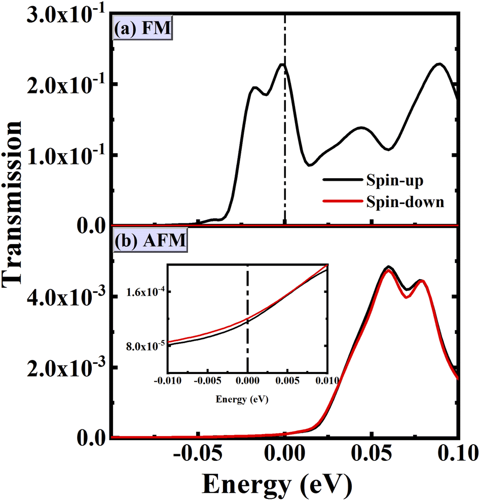 | ||
| Fig. 8 The transmission coefficients versus electron energy at zero bias for the MTJ in FM (a) and AFM (b) alignment. The inset shows the zoomed-in curve around E = 0 (inset chart). Vertical black-dashed line shows the Fermi level. | ||
TMR is a critical parameter to characterize the performance of the MTJ device. According to the formula 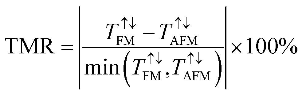 , TMR can be calculated by total transmission coefficients at the Ef level, where
  and
and  refer to total coefficients in FM and AFM alignments, respectively, and
  is the smaller one of the two values. Our calculated
  and
and  are 2.26 × 10⁻¹/9.28 × 10−7 and 1.16 × 10⁻⁴/1.20 × 10−4, respectively, giving a large TMR of 1 × 10³%. The remarkably large TMR value originates from the significant transmission coefficient of the spin-majority channel in FM alignment but small transmission coefficients of both spin-majority and spin-minority channels in AFM alignment.
In Fig. 9, we illustrate the realistic PDOS distributions along the transport direction (z) to underline the tunneling transport mechanism. Along the transmission route, the region from 10 Å to 30 Å represents the central scattering region (red box; Fig. 1). For FM alignment, the spin-up electrons suffer from a lower-height barrier and they can easily cross it, and thus the spin-majority transmission channel is opened (Fig. 9a, yellow sparkles join together to form long strings around the Ef); the spin-down electrons encounter a remarkably higher-height barrier due to a wide band gap of 2ML-CrI3 layers, and thus the spin-minority transmission channel is blocked (Fig. 9b, no yellow sparkles around the Ef). For AFM alignment, the spin-up electrons go across the lower-potential barrier of the left scattering region (Fig. 9c: 10 Å to 20 Å; yellow sparkles around the Ef), and then they meet another potential barrier provided by the bottom CrI3 layer (20 Å to 30 Å; no yellow sparkle around the Ef); it is reversed for the spin-down electrons (Fig. 9d). This observed transport evidence is consistent with the band structure analyses from Fig. 6 and 7, where the spin-dependent band gaps of CrI3 layers are responsible for the spin-dependent barrier height.
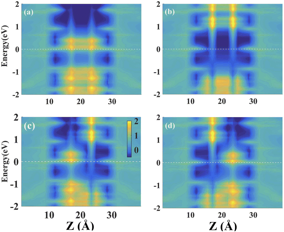 | ||
| Fig. 9 Project density of states (PDOS) along the transport direction (z direction) at equilibrium state in realistic space. Spin-majority (a) and spin-minority (b) states in FM alignment; spin-up (c) and spin-down (d) states in AFM alignment. All the sub-figures have the same color coding values, which are given by the vertical bar. The white-dashed lines at energy = 0 eV denote the Ef. | ||
The spin dependent k‖-resolved transmission coefficients in 2D Brillouin zone (BZ) are calculated at Ef and their contour plots are displayed in Fig. 10, where kx and ky are perpendicular to the transport direction z and the k-grid number is set to be 100 × 100. For FM alignment in Fig. 10a and b, the density of hot spots in the spin majority–majority channel are much larger than those in the spin minority–minority channel, indicating that spin-up electrons have higher transport ability than spin-down electrons, in agreement with the transmission curves shown in Fig. 8a. For example, the topmost hot spot presents a large transmission coefficient of 0.24 at the edge of the BZ in FM alignment. In Fig. 10c and d, although there are little hot spots in both contour plots, their strength is 2–3 orders of magnitude weaker than that of FM alignment, meaning that the tunneling current in AFM alignment would be much smaller than that in FM alignment.
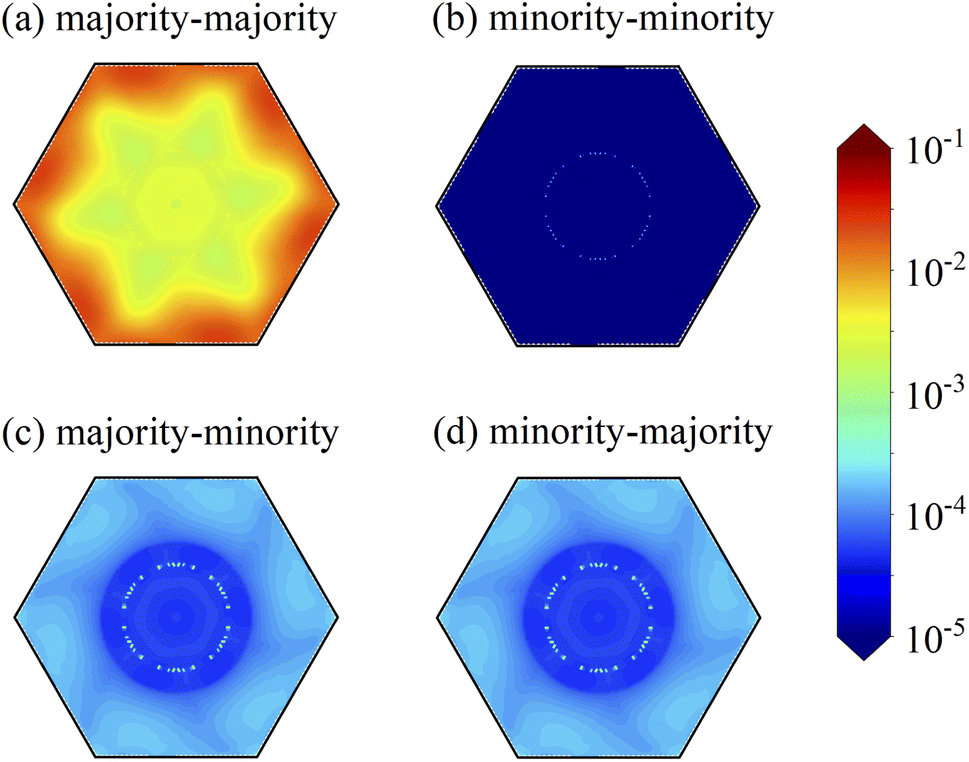 | ||
| Fig. 10 The k‖-resolved transmission coefficient at the Ef in the 2D BZ of the MTJ. kx and ky are perpendicular to the transport direction. (a) and (b) are for the MTJ in FM alignment; (c) and (d) are for MTJ in AFM alignment. | ||
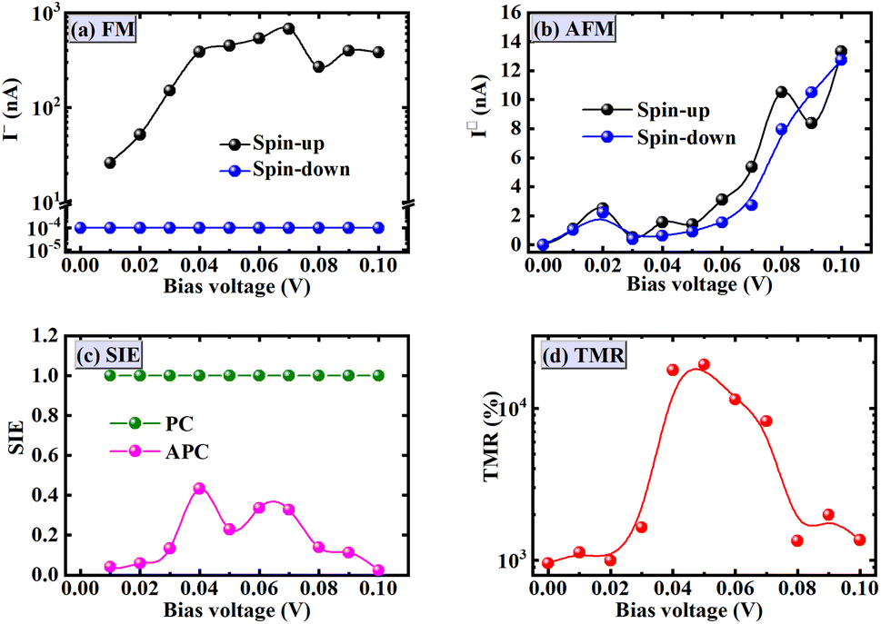 | ||
| Fig. 11 I–V curves in FM alignment (a) and AFM alignment (b); SIE (c) and TMR (d) versus the bias voltage. The solid line is a guide to the trend for the eye. | ||
The spin injection efficiency (SIE) can reveal the degree of spin polarization in transport current, and it can be expressed as: 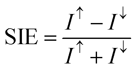 . We displayed the SIE of the FM and AFM alignments in Fig. 11c. The heterostructure maintains 100% SIE in FM alignment, but it shows the largest value of about 40% at bias voltage 0.04–0.07 V in AFM alignment. A large SIE in FM alignment is related to a much larger spin-up current than spin-down current, as shown in Fig. 11a. Using the total current of I↑↓ = I↑ + I↓ in FM and AFM alignments, we calculated TMR according to
  , and showed them versus the bias voltage in Fig. 11d. It is less than 1 × 10³% for V < 0.03 V and dramatically increases to 2 × 10⁴% at 0.05 V, followed by a decrease down to 1 × 10³% again. Compared with Cu|2ML-CrI3|Cu MTJ where 2ML-CrI3 layers synchronously act as the barrier layer and TMR was reported to be 1500%,23 the two Gr layers in our designed MTJ can be an additional barrier layer and they also play the spin-filtering roles. As analyzed in Fig. 6 and 7, the spin-up states are blocked to a certain degree but spin-down can easily cross two graphene layers in FM alignment, while the spin-up/spin-down states are blocked/cross the top-graphene but suffer the opposite effect when they meet the bottom-graphene. This may be the reason that our calculated TMR values are larger than those of Cu|2ML-CrI3|Cu MTJ. The variational trend can be understood with the following reasons: (i) at low bias voltage 0–0.03 V,
  and thus
  are 2 orders larger than
  due to significant blocked roles of AFM 2ML-CrI3 layers on the spin-up/down electrons; (ii) as bias voltage increases from 0.03 V to 0.07 V,
  increases quickly but
  increases slowly, due to the small Dirac-gap (0.2 eV) of the spin-majority channel in FM alignment providing a very low barrier, but large spin-up/down band gaps (3.0 eV) of AFM 2ML-CrI3 layers provide a higher barrier; (iii) further increasing bias voltage (larger than 0.07 V) will assist the spin-down electrons to pass through the barrier of FM 2ML-CrI3 layers.
IV. Conclusions
In summary, we have constructed a vdW-heterostructure with 2ML-CrI3 layers sandwiched between two Gr monolayers, and then used Ag(111) layers as the electrodes in building a vdW-MTJ model to explore the spin transport properties. By employing the DFT and DFT-NEGF methods, structural stability, electronic structures, tunneling conductance, k‖-resolved transmission coefficient, SIE and TMR were investigated. Due to the lattice mismatch between CrI3 and Gr layers as well as the remarkably large Young’s modulus of Gr layer, CrI3 layers in the Gr|2ML-CrI3|Gr heterostructure get stretched. Strong hybridizations of Cr(3d)-eg and I-pz states with Gr-Dirac-cone state allow 2ML-CrI3 layers to show metallic features in the spin-majority channel, for which the Fermi level is located close to the bottom of the upper Hubbard band of the eg manifold; however, the insulator characteristic in the spin-minority channel of CrI3 layers is almost unchanged. This renders the 2ML-CrI3 layers a spin filter for electron tunneling, and consequently, Gr|2ML-CrI3|Gr MTJs shows a perfect spin filter effect and a giant TMR ratio reaching up to 20000%. The physical mechanisms behind the phenomenon are given by analyzing the spin-polarized band structure and k‖-resolved transmission spectra, i.e., large differences of tunneling conductance between FM and AFM alignments are driven by the distinctive electronic structure of two spin transmission channels in 2ML-CrI3 (unobstructed transmission of spin-up channel for a parallel-aligned configuration vs. suppressed transmission of both spin-channels for an antiparallel-aligned configuration). Based on our calculated results, the CrI3-device designed in this study is expected to work in a low field and provide important theoretical guidance for further experimental studies of 2D CrI3-based vdW MTJs, which may gain valuable applications in spintronics.
Author contributions
This manuscript was written through contributions from all authors. All authors have given approval to the final version of the manuscript.Conflicts of interest
All authors declare that they have no conflicts of interest.Acknowledgements
This work was supported by the National Natural Science Foundation of China (11874306, 12174320), and the Natural Science Foundation of Chongqing (CSTC2021jcyj-msxm1946, cstc2022ycjh-bgzxm0127). We gratefully acknowledge HZWTECH for providing computational facilities. Hongkuan Yuan thanks Kui Gong, Yibin Hu and Yin Wang (all from HZWTECH) for help and discussions regarding this study.References
- C. Gong and X. Zhang, Two-dimensional magnetic crystals and emergent heterostructure devices, Science, 2019, 363, eaav4450 CrossRef CAS.
- L. Zhang, J. Zhou, H. Li, L. Shen and Y. P. Feng, Recent progress and challenges in magnetic tunnel junctions with 2D materials for spintronic applications, Appl. Phys. Rev., 2021, 8, 021308 CAS.
- D. L. Cortie, G. L. Causer, K. C. Rule, H. Fritzsche, W. Kreuzpaintner and F. Klose, Two-dimensional magnets forgotten history and recent progress towards spintronic applications, Adv. Funct. Mater., 2020, 30, 1901414 CrossRef CAS.
- S. J. Liang, B. Cheng, X. Cui and F. Miao, Van der Waals heterostructures for high-performance device applications challenges and opportunities, Adv. Mater., 2020, 32, 1903800 CAS.
- J. Chu, Y. Wang, X. Wang, K. Hu, G. Rao, C. Gong, C. Wu, H. Hong, X. Wang, K. Liu, C. Gao and J. Xiong, 2D polarized materials: Ferromagnetic, ferrovalley, ferroelectric materials, and related heterostructures, Adv. Mater., 2021, 33, 2004469 CrossRef CAS PubMed.
- S. Yang, T. Zhang and C. Jiang, Van der Waals magnets material family, detection and modulation of magnetism, and perspective in spintronics, Adv. Sci., 2021, 8, 2002488 CrossRef CAS PubMed.
- D. R. Klein, D. MacNeill, J. L. Lado, D. Soriano, E. NavarroMoratalla, K. Watanabe, T. Taniguchi, S. Manni, P. Canfield, J. Fernandez-Rossier and P. Jarillo-Herrero, Probing magnetism in 2D van der Waals crystalline insulators via electron tunneling, Science, 2018, 360, 1218–1222 CrossRef CAS.
- T. Song, X. Cai, M. W. Y. Tu, X. Zhang, B. Huang, N. P. Wilson, K. L. Seyler, L. Zhu, T. Taniguchi, K. Watanabe, M. A. Mcguire, D. H. Cobden, D. Xiao, W. Yao and X. Xu, Giant tunneling magnetoresistance in spin-filter van der Waals heterostructures, Science, 2018, 360, 1214–1218 CrossRef CAS.
- Z. Wang, I. Gutiérrez-Lezama, N. Ubrig, M. Kroner, M. Gibertini, T. Taniguchi, K. Watanabe, A. Imamoğlu, E. Giannini and A. F. Morpurgo, Very large tunneling magnetoresistance in layered magnetic semiconductor CrI3, Nat. Commun., 2018, 9, 2516 CrossRef PubMed.
- H. H. Kim, B. Yang, T. Patel, F. Sfigakis, C. Li, S. Tian, H. Lei and A. W. Tsen, One million percent tunnel magnetoresistance in a magnetic van der Waals heterostructure, Nano Lett., 2018, 18, 4885–4890 CrossRef CAS.
- B. Huang, G. Clark, E. Navarro-Moratalla, D. R. Klein, R. Cheng, K. L. Seyler, D. Zhong, E. Schmidgall, M. A. McGuire, D. H. Cobden and W. Yao, Layer-dependent ferromagnetism in a van der Waals crystal down to the monolayer limit CrI3, Nature, 2017, 546, 270–273 CrossRef CAS.
- C. Gong, L. Li, Z. Li, H. Ji, A. Stern, Y. Xia, T. Cao, W. Bao, C. Wang, Y. Wang and Z. Q. Qiu, Discovery of intrinsic ferromagnetism in two-dimensional van der Waals crystals, Nature, 2017, 546, 265–269 CrossRef CAS.
- M. Bonilla, S. Kolekar, Y. Ma, H. C. Diaz, V. Kalappattil, R. Das, T. Eggers, H. R. Gutierrez, M. H. Phan and M. Batzill, Strong room-temperature ferromagnetism in VSe2 monolayers on van der Waals substrates, Nat. Nanotechnol., 2018, 13, 289 CrossRef CAS.
- Z. Fei, B. Huang, P. Malinowski, W. Wang, T. Song, J. Sanchez, W. Yao, D. Xiao, X. Zhu, A. F. May, W. Wu, D. H. Cobden, J. Chu and X. Xu, Two-dimensional itinerant ferromagnetism in atomically thin Fe3GeTe2, Nat. Mater., 2018, 17, 778 CrossRef CAS PubMed.
- Y. Deng, Y. Yu, Y. Song, J. Zhang, N. Z. Wang, Z. Sun, Y. Yi, Y. Z. Wu, S. Wu, J. Zhu, J. Wang, X. H. Chen and Y. Zhang, Gate-tunable room-temperature ferromagnetism in two-dimensional Fe3GeTe2, Nature, 2018, 563, 94 CrossRef CAS PubMed.
- H. H. Kim, B. Yang, S. Tian, C. Li, G. X. Miao, H. Lei and A. W. Tsen, Tailored tunnel magnetoresistance response in three ultrathin chromium trihalides, Nano Lett., 2019, 19, 5739–5745 CrossRef CAS PubMed.
- T. Song, M. W. Y. Tu, C. Carnahan, X. Cai, T. Taniguchi, K. Watanabe, M. A. McGuire, D. H. Cobden, D. Xiao, W. Yao and X. Xu, Voltage control of a van der Waals spin-filter magnetic tunnel junction, Nano Lett., 2019, 19, 915–920 CrossRef CAS PubMed.
- Z. Qiu, M. Holwill, T. Olsen, P. Lyu, J. Li, H. Fang, H. Yang, M. Kashchenko, K. S. Novoselov and J. Lu, Visualizing atomic structure and magnetism of 2D magnetic insulators via tunneling through graphene, Nat. Commun., 2021, 12, 70 CrossRef CAS PubMed.
- B. Yang, X. Zhang, H. Yang, X. Han and Y. Yan, Strain controlling transport properties of heterostructure composed of monolayer CrI3, Appl. Phys. Lett., 2019, 114, 192405 CrossRef.
- J. J. Heath, M. Costa, M. Buongiorno-Nardelli and M. A. Kuroda, Role of quantum confinement and interlayer coupling in CrI3-graphene magnetic tunnel junctions, Phys. Rev. B, 2020, 101, 195439 CrossRef CAS.
- D. Ghazaryan, M. T. Greenaway, Z. Wang, V. H. Guarochico-Moreira, I. J. Vera-Marun, J. Yin, Y. Liao, S. V. Morozov, O. Kristanovski, A. I. Lichtenstein, M. I. Katsnelson, F. Withers, A. Mishchenko, L. Eaves, A. K. Geim, K. S. Novoselov and A. Misra, Magnon-assisted tunneling in van der Waals heterostructures based on CrBr3, Nat. Electron., 2018, 1, 344–349 CrossRef CAS.
- L. Pan, L. Huang, M. Zhong, X. W. Jiang, H. X. Deng, J. Li, J. B. Xia and Z. Wei, Large tunneling magnetoresistance in magnetic tunneling junctions based on two-dimensional CrX3 (X = Br, I) monolayers, Nanoscale, 2018, 10, 22196 RSC.
- T. R. Paudel and E. Y. Tsymbal, Spin filtering in CrI3 tunnel junctions, ACS Appl. Mater. Interfaces, 2019, 11, 15781–15787 CrossRef CAS PubMed.
- Z. Yan, R. Zhang, X. Dong, S. Qi and X. Xu, Significant tunneling magnetoresistance and excellent spin filtering effect in CrI3-based van der Waals magnetic tunnel junctions, Phys. Chem. Chem. Phys., 2020, 22, 14773 RSC.
- F. Li, B. Yang, Y. Zhu, X. Han and Y. Yan, Four distinct resistive states in van der Waals full magnetic 1T-VSe2/CrI3/1T-VSe2 tunnel junction, Appl. Surf. Sci., 2020, 505, 144648 CrossRef CAS.
- F. Li, B. Yang, Y. Zhu, X. Han and Y. Yan, Ultrahigh tunneling magnetoresistance in van der Waals and lateral magnetic tunnel junctions formed by intrinsic ferromagnets Li0.5CrI3 and CrI3, Appl. Phys. Lett., 2020, 117, 022412 CrossRef CAS.
- Z. Wang, D. Sapkota, T. Taniguchi, K. Watanabe, D. Mandrus and A. F. Morpurgo, Tunneling spin valves based on Fe3GeTe2/hBN/Fe3GeTe2 van der Waals heterostructures, Nano Lett., 2018, 18, 4303–4308 CrossRef CAS.
- X. Li, J. T. Lu, J. Zhang, L. You, Y. Su and E. Y. Tsymbal, Spin-Dependent transport in van der Waals magnetic tunnel junctions with Fe3GeTe2 electrodes, Nano Lett., 2019, 19, 5133–5139 CrossRef CAS.
- L. Zhang, T. Li, J. Li, Y. Jiang, J. Yuan and H. Li, Perfect spin filtering effect on Fe3GeTe2-based Van der Waals magnetic tunnel junctions, J. Phys. Chem. C, 2020, 124, 27429–27435 CrossRef CAS.
- H. Lin, F. Yan, C. Hu, Q. Lv, W. Zhu, Z. Wang, Z. Wei, K. Chang and K. Wang, Spin-Valve effect in Fe3GeTe2/MoS2/Fe3GeTe2 van der Waals heterostructures, ACS Appl. Mater. Interfaces, 2020, 12, 43921–43926 CrossRef CAS.
- W. Yang, Y. Cao, J. Han, X. Lin, X. Wang, G. Wei, C. Lv, A. Bournel and W. Zhao, Spin-filter induced large magnetoresistance in 2D van der Waals magnetic tunnel junctions, Nanoscale, 2021, 13, 862 RSC.
- J. Zhou, J. Qiao, C. G. Duan, A. Bournel, K. L. Wang and W. Zhao, Large tunneling magnetoresistance in VSe2/MoS2 magnetic tunnel junction, ACS Appl. Mater. Interfaces, 2019, 11, 17647–17653 CrossRef CAS PubMed.
- H. Zhou, Y. Zhang and W. Zhao, Tunable tunneling magnetoresistance in van der Waals magnetic tunnel junctions with 1T-CrTe2 electrodes, ACS Appl. Mater. Interfaces, 2021, 13, 1214–1221 CrossRef CAS.
- C. Cardoso, D. Soriano, N. A. Garc-Martnez and J. Fernndez-Rossier, Van der Waals spin valves, Phys. Rev. Lett., 2018, 121, 067701 CrossRef CAS.
- G. Kresse and J. Hafner, Norm-conserving and ultrasoft pseudopotentials for first-row and transition elements, J. Phys.: Condens. Matter, 1994, 6, 8245 CrossRef CAS.
- G. Kresse and D. Joubert, From ultrasoft pseudopotentials to the projector augmented-wave method, Phys. Rev. B: Condens. Matter Mater. Phys., 1999, 59, 1758 CrossRef CAS.
- D. Hobbs, G. Kresse and J. Hafner, Fully unconstrained noncollinear magnetism within the projector augmented-wave method, Phys. Rev. B: Condens. Matter Mater. Phys., 2000, 62, 11556 CrossRef CAS.
- M. Marsman and J. Hafner, Broken symmetries in the crystalline and magnetic structures of γ-iron, Phys. Rev. B: Condens. Matter Mater. Phys., 2002, 66, 224409 CrossRef.
- J. P. Perdew, J. A. Chevary, S. H. Vosko, K. A. Jackson, M. R. Pederson, D. J. Singh and C. Fiolhais, Atoms, molecules, solids, and surfaces: applications of the generalized gradient approximation for exchange and correlation, Phys. Rev. B: Condens. Matter Mater. Phys., 1992, 46, 6671 CrossRef CAS.
- J. P. Perdew, K. Burke and M. Ernzerhof, Generalized gradient approximation made simple, Phys. Rev. Lett., 1996, 77, 3865 CrossRef CAS PubMed.
- P. E. Blöchl, Projector augmented-wave method, Phys. Rev. B: Condens. Matter Mater. Phys., 1994, 50, 17953 CrossRef.
- A. Dal Corso and A. Mosca Conte, Spin-orbit coupling with ultrasoft pseudopotentials: Application to Au and Pt, Phys. Rev. B: Condens. Matter Mater. Phys., 2005, 71, 115106 CrossRef.
- S. Grimme, Semiempirical GGA-type density functional constructed with a long-range dispersion correction, J. Comput. Chem., 2006, 27, 1787 CrossRef CAS PubMed.
- L. Wang, T. Maxisch and G. Ceder, Oxidation energies of transition metal oxides within the GGA+U framework, Phys. Rev. B: Condens. Matter Mater. Phys., 2006, 73, 195107 CrossRef.
- O. Bengone, M. Alouani, P. Blöchl and J. Hugel, Implementation of the projector augmented-wave LDA+U method: Application to the electronic structure of NiO, Phys. Rev. B: Condens. Matter Mater. Phys., 2000, 62, 16392 CrossRef CAS.
- A. Rohrbach, J. Hafner and G. Kresse, Molecular adsorption on the surface of strongly correlated transition-metal oxides: A case study for CO/NiO (100), Phys. Rev. B: Condens. Matter Mater. Phys., 2004, 69, 075413 CrossRef.
- J. Kim, K. W. Kim, B. Kim, C. J. Kang, D. Shin, S. H. Lee, B. C. Min and N. Park, Exploitable magnetic anisotropy of the two-dimensional magnet CrI3, Nano Lett., 2020, 20, 929–935 CrossRef CAS.
- M. A. McGuire, H. Dixit, V. R. Cooper and B. C. Sales, Coupling of crystal structure and magnetism in the layered, ferromagnetic insulator CrI3, Chem. Mater., 2015, 27, 612–620 CrossRef CAS.
- J. Taylor, H. Guo and J. Wang, Ab initio modeling of open systems: Charge transfer, electron conduction, and molecular switching of a C-60 device, Phys. Rev. B: Condens. Matter Mater. Phys., 2001, 63, 121104 CrossRef.
- A. P. Jauho, N. S. Wingreen and Y. Meir, Time-dependent transport in interacting and noninteracting resonant-tunneling systems, Phys. Rev. B: Condens. Matter Mater. Phys., 1994, 50, 5528–5544 CrossRef CAS.
- J. Taylor, H. Guo and J. Wang, Ab initio modeling of quantum transport properties of molecular electronic devices, Phys. Rev. B: Condens. Matter Mater. Phys., 2001, 63, 245407 CrossRef.
- Y. Meir and N. S. Wingreen, Landauer formula for the current through an interacting electron region, Phys. Rev. Lett., 1992, 68, 2512 CrossRef PubMed.
- J. M. Soler, E. Artacho, J. D. Gale, A. Garcia, J. Junquera, P. Ordejon and D. Sanchez-Portal, The SIESTA method for ab initio order-N materials simulation, J. Phys.: Condens. Matter, 2002, 14, 2745–2779 CrossRef CAS.
- H. Wang, J. Zhou, X. Liu, C. Yao, H. Li, L. Niu, Y. Wang and H. Yin, Spin transport through a junction entirely consisting of molecules from first principles, Appl. Phys. Lett., 2017, 111, 172408 CrossRef.
- W. B. Zhang, Q. Qu, P. Zhu and C. H. Lam, Robust intrinsic ferromagnetism and half semiconductivity in stable two-dimensional single-layer chromium trihalides, J. Mater. Chem. C, 2015, 3, 12457–12468 RSC.
- T. Liu, N. Zhou, X. Li, G. Zhu, X. Wei, J. Cao and Z. Yang, Prediction of colossal magnetocrystalline anisotropy for transition metal triiodides, J. Phys.: Condens. Matter, 2019, 31, 295801 CrossRef CAS.
- C. X. Huang, J. S. Feng, F. Wu, D. Ahmed, B. Huang, H. J. Xiang, K. M. Deng and E. Kan, Toward intrinsic room-temperature ferromagnetism in two dimensional semiconductors, J. Am. Chem. Soc., 2018, 140, 11519–11525 CrossRef CAS.
- J. Zhang, B. Zhao, T. Zhou, Y. Xue and C. Ma, Strong magnetization and Chern insulators in compressed graphene/CrI3 van der Waals heterostructures, Phys. Rev. B, 2018, 97, 085401 CrossRef CAS.
- J. F. Dillon and C. E. Olson, Magnetization, resonance, and optical properties of the ferromagnet CrI3, J. Appl. Phys., 1965, 36, 1259–1260 CrossRef CAS.
- A. V. Krukau, O. A. Vydrov, A. F. Izmaylov and G. E. Scuseria, Influence of the exchange screening parameter on the performance of screened hybrid functionals, J. Chem. Phys., 2006, 125, 224106 CrossRef PubMed.
- N. Sivadas, S. Okamoto, X. Xu, C. J. Fennie and D. Xiao, Stacking-dependent magnetism in bilayer CrI3, Nano Lett., 2018, 18, 7658–7664 CrossRef CAS PubMed.
- P. Jiang, C. Wang, D. Chen, Z. Zhong, Z. Yuan, Z. Y. Lu and W. Ji, Stacking tunable interlayer magnetism in bilayer CrI3, Phys. Rev. B, 2019, 99, 144401 CrossRef CAS.
- R. Xu and X. Zou, Electric Field-Modulated Magnetic Phase Transition in van der Waals CrI3 Bilayers, J. Phys. Chem. Lett., 2020, 11, 3152 CrossRef CAS PubMed.
- F. Zheng, J. Zhao, Z. Liu, M. Li, M. Zhou, S. Zhang and P. Zhang, Tunable spin states in the two-dimensional magnet CrI3, Nanoscale, 2018, 10, 14298 RSC.
- A. Politano and G. Chiarello, Probing the Young’s modulus and Poissons ratio in graphene/metal interfaces and graphite: a comparative study, Nano Res., 2015, 8, 1847 CrossRef CAS.
Footnotes |
| † Electronic supplementary information (ESI) available. See https://doi.org/10.1039/d2ra02988j |
| ‡ Equal contribution author. |
| This journal is © The Royal Society of Chemistry 2022 |