 Open Access Article
Fabrication of two Se/CsPbBr3 heterojunctions structures for self-powered UV–visible photodetectors†
Jiaojiao Liu ab and
Jie Zhang
 *ab
*ab
aSchool of Electronic and Information Engineering, Changshu Institute of Technology, Changshu 215500, China. E-mail: liujiaojiao@cslg.edu.cn; zj2016@cslg.edu.cn
bSuzhou Key Laboratory of Advanced Lighting and Display Technologies, China
First published on 24th November 2022
Abstract
It has been a universal route for enhanced photoelectric performance in photodetectors by constructing a heterojunction that is conductive for suppressing recombination of photogenerated carriers and promoting collection efficiency, and probably producing self-powered capability. However, the dependence of the built-in electric field distributions created by the heterojunction on photodetector performance has rarely been investigated. Herein, two kinds of self-powered UV–visible photodetectors with different device architectures based on single Se wire and CsPbBr3 particles are facilely fabricated and compared. It is found that both the two photodetectors show excellent self-powered operating properties, fast response and binary response. However, due to the different distributions of built-in electric field caused by device architectures, it yields a significant photovoltaic voltage distinction and different responsivity and detectivity spectra for the Se/CsPbBr3 photodetectors. These results are conductive to guide the design of self-powered heterojunction photodetectors by regulating the built-in electric field distributions.
1. Introduction
Photodetectors (PDs), which can detect irradiation directly by transforming light signals into electrical signals, have attracted much attention in the past decades due to their wide applications in versatile fields including environmental monitoring, space exploration, light communication, chemical and biological analysis, imaging etc.1–6 Among these PDs, self-powered PDs have shown great potentials as they are effective, reliable and most importantly energy-saving. Differing from many PDs which can only operate under an external power source, self-powered PDs can work under zero bias by exploiting the photovoltaic effect from p–n junctions, heterojunctions or Schottky junction under light illumination. The built-in electric field created by these structures contributes to its photocurrent response under zero bias. Therefore, self-powered PDs have attracted more and more attention as the increasing emphasis on energy conservation. Recently researchers have developed versatile self-powered PDs with improved performance or integrated features.7–12 For example, Wang's group has reported that a fully transparent ultraviolet (UV) PD based on TiO2 thin film can work without external power sources due to the asymmetric Schottky junctions.13 Moreover, an UV communication system has been developed, showing good capability of data communication. Among these devices, the design of device architectures is of particularly importance for fabricating self-powered PDs. Therefore, it is necessary to study the influence of device architectures of on their photoelectric performance and in-depth mechanism for self-powered PDs.Considering the materials utilized to fabricate different types of high performance PDs, intrinsic p-type semiconductor selenium (Se) is a prospective candidate and has attracted many attentions for its excellent physical properties, such as high hole mobility (∼0.14 cm2 V−1 s−1), high intrinsic carrier concentration (∼9.35 × 1016 cm−3), fast response time and nonlinear optical responses.14–16 The band gap of approximately 1.7 eV means that Se possesses broadband photoresponse from visible to ultraviolet region. Researchers have fabricated several Se PDs based on various micro/nanostructures, such as nanoscale thin films, micro/nanowire, microtubes and nanosheets.17–21 Se microwires synthesized by chemical vapor deposition features low cost, sound crystallization, and more importantly they are easy to build Se-based heterojunction PDs by combining with other materials. Hu et al. has fabricated a single Se microwire broadband PD with responsivity enhancement by sputtering Au nanoparticles, which is interpreted by the surface plasmon coupling effect.19 In Yu et al.'s research, self-powered broadband PD of single Se microwire with half-coated conductive polymers [polyaniline (PANI), polypyrrole (PPy) and poly (3,4-ethylenedioxythiophene) (PEDOT)] have achieved via a facile and low-cost in situ polymerization method.20 These integrated PDs all show excellent self-powered behaviors under UV-vis light illumination. However, the effect of device architectures on the Se-based PD performance has rarely been investigated.
Compared with single-element semiconductors, the presence of multi-element semiconductor materials with variety of bandgaps show more possibilities for obtaining all-optical functions and may partly enhance the photodetection performance. As structure impinges on the properties, it is expected enhanced properties can be realized by adjusting the structures in the composites. Among them, perovskite semiconductors gradually show excellent photoelectric properties due to their unique material properties.22,23 For example, Ding's group has reported the design and fabrication of high-performance visible/near-infrared dual color PDs based on CH3NH3PbBr3 perovskite hybrid films.23 Recently, fully inorganic cesium lead halide perovskite (CsPbX3, X = Cl, Br, I) nanocrystals have been emerging as an important class of semiconductor materials, which has immediately gained tremendous interest since the pioneering works.24 They possess superior photophysical properties and wide potential applications in optoelectronic devices.25,26
Particularly, CsPbBr3 perovskite with high stability and simple fabrication process has been combined with various p-type semiconductors to construct different heterostructures for photodetecting applications, such as CsPbBr3/ZnO, CsPbBr3/TiO2, CsPbBr3/SnO2.27–29 Fang et al. has reported that SnO2/CsPbBr3 PDs with two different structures have both outstanding photoelectric performances. A kind of SnO2/CsPbBr3 PDs has been constructed by a single SnO2 millimeter wire decorated with CsPbBr3 particles, which shows self-powered characteristic and fast photoresponse (0.03 ms/1.94 ms). Meanwhile SnO2 microwires combined with CsPbBr3 have been also utilized to fabricate another kind of SnO2/CsPbBr3 PDs, exhibiting dual wavelength response (320 and 520 nm) under zero voltage bias.29 Wang's group has demonstrated a high-performance self-powered CsPbBr3 perovskite PD based on an all-inorganic structure. The configuration of the PD consists of glass/FTO/ZnO NRs/CsPbBr3/MoO3/Au. The constructed self-powered devices show high performance with the responsivity of 0.3 A W−1, detectivity of 1.15 × 1013 cm Hz1/2 W−1 and on/off ratio of 4.5 × 102.30 Li et al. has developed a high-performance, self-powered and flexible photothermoelectric effect PDs based on laser-scribed reduced graphene oxide/CsPbBr3 (100 mA W−1 for 405 nm and 10 mA W−1 for 118 μm).31 The device exhibits ultrabroadband photodetection and high responsivity covering from ultraviolet to terahertz range at zero bias voltage. Accordingly, the construction of CsPbBr3-based heterojunctions, in which the built-in electric field as a driving force can suppress recombination of photogenerated carriers and then promote collection efficiency, produces a wonderful self-powered characteristic. However, the dependence of the built-in electric field distributions created by the heterojunction on PD performance has rarely been investigated. Additionally, there exist few works focusing on the PD structures based on CsPbBr3 and Se semiconductors. Therefore, we have constructed two CsPbBr3/Se structures to exploit PD performance in depth.
In this work, millimeter Se wires are synthetized by chemical vapor deposition. The ultralong wire enable us to easily fabricate heterojunction PDs with different architectures. Two kind of PDs architected with fully-covered CsPbBr3 on Se wire (denoted as Se/CsPbBr3/1) and partially-covered CsPbBr3 on Se wire (denoted as Se/CsPbBr3/2) heterojunctions are fabricated and compared. It is found that both PDs possess self-powered features, fast response and binary response. However, the Se/CsPbBr3/2 PDs present much higher open-circuit voltage (0.9 V) than that with Se/CsPbBr3/1 PDs (0.1 V). Moreover, it is observed that the Se/CsPbBr3/2 device shows a rapid rise from 600 to 500 nm, but the Se/CsPbBr3/1 device shows an obvious drop from 600 to 500 nm in responsivity and detectivity. The underlying mechanisms are analyzed and are suggested to be related to different distributions of the built-in electric field at the interface of Se and CsPbBr3. This study provides guidance for constructing performance-tunable, self-powered heterojunction PDs by regulating the device architectures.
2. Results and discussion
X-ray diffraction (XRD) patterns are used to determine the crystallographic nature of the single Se wire and CsPbBr3 particles. Se wires were synthesized via a typical chemical vapor deposition method and CsPbBr3 particles are obtained by heating the DMSO solution which contains CsBr and PbBr2 (detailed in the Experimental section). As shown in Fig. 1a, a high crystal quality is proved by the strong and sharp diffraction peak of the single Se wire at the degree of 23.5°, corresponding to the (100) crystal face of hexagonal Se with lattice parameters of a = b = 4.364 Å, c = 4.959 Å (JCPDS No. 65-1876). The as-prepared high-quality Se wires provide a promising candidate to integrate with other semiconductor materials for various device structures. Fig. 1b exhibits the diffraction peaks of the CsPbBr3 particles, which match well with the cesium lead bromide phase of CsPbBr3 with lattice parameters of a = b = c = 5.83 Å (JCPDF No. 54-0752), confirming the crystallinity and purity of the as-obtained sample. The main diffraction peaks of CsPbBr3 particles located at 21.6°, 30.6°, 37.8° and 43.9° are attributed to the (110), (200), (211) and (220) crystal facets of the CsPbBr3.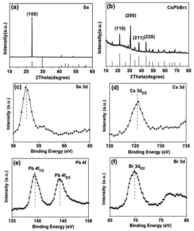 | ||
| Fig. 1 XRD patterns: (a) Se wire (b) CsPbBr3 particles XPS spectra: (c) Se 3d (d) Cs 3d (e) Pb 4f (f) Br 3d. | ||
In order to investigate the composition and electronic states of the as-prepared Se wires and CsPbBr3 particles, X-ray photoelectron spectroscopy (XPS) measurements were performed by using element C for calibration. Fig. 1c displays the XPS spectrum of the Se sample. The binding energy peak emerging at 52.6 eV reveals the presence of elemental Se (related to Se 3d5/2). Fig. 1d–f present the spectra of elements in CsPbBr3 sample. The binding energy at 725.4 eV is corresponding to Cs 3d5/2 (Fig. 1d). The two binding energy peaks located at around 139.5 eV and 144.4 eV can be assigned to Pb 4f7/2 and Pb 4f5/2, respectively, revealing the existence of Pb2+ in CsPbBr3 samples (Fig. 1e). The binding energy peaks located at 69.9 eV can be ascribed to the spin orbital splitting photoelectrons of Br 3d5/2 (Fig. 1f). These results further demonstrate the coexistence of element Se, Cs, Pb and Br in the samples. All these characterizations suggest that the as-obtained Se wires and CsPbBr3 particles possess good crystallinity.
Fig. 2 displays the scanning electron microscopy (SEM) images of three samples with different magnifications. As shown in Fig. 2a and c, part of single Se wire with a mean diameter of 50 μm is observed. The surfaces are smooth, indicating the high purity of Se products. The CsPbBr3 solution was dropped onto the Se wire and heated in the surrounding environment. After the evaporation of the solvent, the Se/CsPbBr3 composites were formed. The enlarged image of single cuboid CsPbBr3 particle on Se wire in Fig. 2b demonstrates that the CsPbBr3 particle was crystallized and grown tightly on the surface of Se wire. In Fig. 2d, many CsPbBr3 particles partially covered and tightly attached to Se wire, forming Se/CsPbBr3 composites. It is observed in Fig. 2d that the single Se wire has a length longer than 1 mm. The aspect ratio of Se wires in the composites can achieve more than 20, which shows the anisotropism of Se products and indicates their preferential growth direction of (100). The ultralong wire enables assembling different heterostructures easily. The pure CsPbBr3 particles with an average diameter of around 10 μm are observed as accumulating together, as given in Fig. 2e and f. The simplicity of the preparation of CsPbBr3 particles will permit promising use of Se/CsPbBr3 composites for fundamental studies and potential applications.
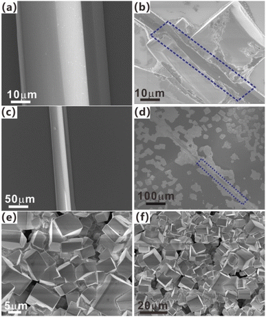 | ||
| Fig. 2 SEM images of (a and c) single Se wire (b and d) Se/CsPbBr3 composites and (e and f) CsPbBr3 particles with different magnification. | ||
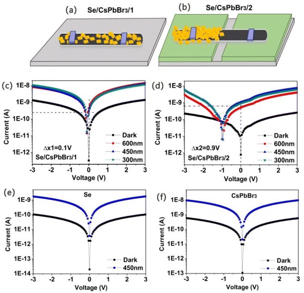
The schematic diagrams of the construction of two different Se/CsPbBr3 heterojunction are depicted in Fig. 3a and b, respectively. During the fabrication of Se/CsPbBr3/1 PD, a single Se wire is placed on a glass substrate and the CsPbBr3 solution is dropped onto it. As the DMSO solvent evaporation under heat treatment, CsPbBr3 crystallizes and is closely tied to Se wire. For the fabrication of Se/CsPbBr3/2 PD, a single Se wire is laid across a small gap between two separate pieces of glass before the CsPbBr3 solution is dropped. After annealing and crystallizing, the Se/CsPbBr3/2 heterojunction is formed. Two small indium pieces were pressed onto the Se/CsPbBr3 composites as the electrodes to build the device. The photoelectric properties of the as-prepared devices were then investigated at room temperature by using a two-probe method. Typical current–voltage (I–V) curves of the two Se/CsPbBr3 PDs in logarithmic plot are displayed in Fig. 3c and d in the dark and upon 600 nm, 450 nm and 300 nm light illumination under the bias of 3 V. Both Se/CsPbBr3 PDs show obvious differences in photocurrents and dark currents. The photocurrents of the Se/CsPbBr3/1 and the Se/CsPbBr3/2 devices can reach 10 nA and 6 nA at bias of 3 V under 450 nm light illumination, which are ten and twenty times as high as that in the dark, respectively. The Se/CsPbBr3/1 PD has higher photocurrents, but the Se/CsPbBr3/2 photodetector shows a much lower dark current and thus a higher photo-to-dark current ratio (Fig. 3d). Noticeably, the relatively high photocurrents of about 0.4 nA under 450 nm light for Se/CsPbBr3/1 and Se/CsPbBr3/2 heterojunction existing at nominal zero bias indicate both devices can operate without an external driving voltage. By comparison in Fig. 3e and f, the I–V curves for pure Se wire and CsPbBr3 particles indicate that both PDs have photoresponse performance, but show no self-powered properties. Therefore, the self-powered behavior in the Se/CsPbBr3 composites mainly results from the formation of heterojunctions between Se wire and CsPbBr3 particles due to the internal photovoltaic effect. More importantly, there are significant differences between the two Se/CsPbBr3 PDs. For the photocurrents at bias of 3 V upon 600 nm light, the photocurrent of Se/CsPbBr3/1 is very close to that upon 450 and 300 nm light illumination, but the photocurrent of Se/CsPbBr3/2 is much lower under the same test condition. For the open-circuit voltage, the Se/CsPbBr3/1 PD only have 0.1 V, but the Se/CsPbBr3/2 PD show a much larger value of 0.9 V. This indicates a much stronger built-in electric field formed between Se wire and CsPbBr3 particles for the Se/CsPbBr3/2 PD than the Se/CsPbBr3/1 PD. In addition, both devices have higher photocurrents than that of pure Se wire. These results demonstrate that the composites devices not only show enhanced photoelectric properties, but also exhibit self-powered characteristics.
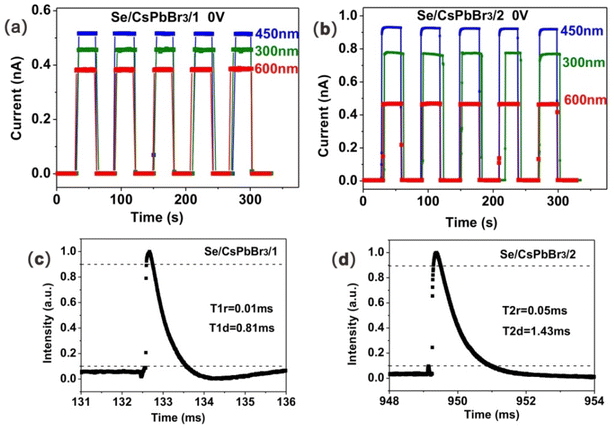
Fig. 4a and b show the time–dependent current (I–t) tests under 600 nm, 450 nm and 300 nm light at 0 V. Under each cycle of switching on, the current of Se/CsPbBr3/1 PD instantly increases to the value of around 0.38 nA (0.52 nA and 0.45 nA) and falls back dramatically to the original value of about 1 pA when the 600 nm (450 nm, 300 nm) light is off. The on/off ratio of this device, defined as the ratio of photocurrent to dark current (Iph/Id) of the photodetector, is calculated to be about 400 at zero bias. The current of Se/CsPbBr3/2 rises to 0.46 nA, 0.88 nA and 0.74 nA, and then declines as with 600 nm, 450 nm and 300 nm light on and off respectively. The results also confirm the stability and repeatability of the devices. The I–t curves correspond well with the I–V curves, yielding stable and repeatable self-powered characteristics at zero bias.
To better illustrate the time resolved properties of the two devices, a quick response measure system is applied and pulse responses of Se/CsPbBr3/1 and Se/CsPbBr3/2 PDs are given in Fig. 4c and d. The quick response measure system uses a pulsed YAG:Nd laser as a light source, the voltage of series resistor as a function of time is recorded by the oscilloscope. When the pulse laser irradiates upon the PDs, the resistance of sample decreases, leading to the rising of partial voltage on series resistor. The photoresponse of both the two devices are very fast under the bias of 0 V. For the Se/CsPbBr3/1 device, the rise/decay time is estimated to be 0.01/0.81 ms (Fig. 4c). This performance for Se/CsPbBr3/2 device is a little bit worse, with the rise/decay time of 0.05/1.43 ms. It is evident that the devices based on Se wire and CsPbBr3 particles show ultrafast response speed. Especially for the Se/CsPbBr3/1 heterojunction, the rise time can reach sub-millisecond magnitude, which is the fastest response time for Se based PDs, to our best knowledge. Zeng's group has reported the rise and decay time of CsPbBr3/ZnO PDs are 0.88/1.53 ms, respectively.27 Fang et al. has proposed a simple method for fabrication high performance self-powered CsPbBr3/CuI photodetector with the rise time and the decay time are 20 μs and 1.85 ms. This response time is significantly faster than those reported on CsPbBr3-based PD.32
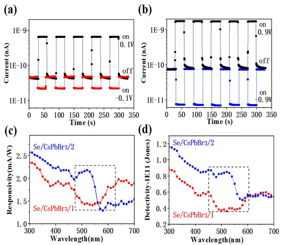
To further explore the response characteristics of the two Se/CsPbBr3 composites devices, their binary response is examined at different bias voltages at a wavelength of 450 nm light illumination. Different bias (−0.1 V and 0.1 V, −0.9 V and 0.9 V) are applied according to their open-circuit voltages (Fig. 3c and d). Interestingly, As depicted in Fig. 5a and b, the Se/CsPbBr3/1 and the Se/CsPbBr3/2 PDs all show that the dark currents are higher than the photocurrents under −0.1 V and −0.9 V, respectively, whereas the dark currents are lower than photocurrents under 0.1 V and 0.9 V. The I–t curve under negative and positive bias all reveal that on/off switching is repeatable and stable. This kind of the positive and negative response inversion is called binary response, which can meet many practical needs, such as optical communications, machine vision etc.31 This interesting result provides an additional pathway to design self-powered PDs with binary response.
Fig. 5 further reveals the photoelectric properties of Se/CsPbBr3 composite PDs with different structures. The spectral responsivity (Rλ) and detectivity (D*) are key parameters to evaluate the performance of a PD. The responsivity is defined as the photocurrent per unit of incident power, indicating how efficiently a detector responds to optical signals. It is usually calculated according to the following equation:  where Iph is the photocurrent, Id is the dark current, Pλ is light power density and S is the effective area under irradiation, λ is the exciting wavelength and e is the electronic charge. The detectivity (typically quoted in Jones) reflects the ability to detect weak signals from the noise environment. Considering the major contributor of background noise is the shot noise from the dark current, the detectivity can be expressed as:
  The responsivities of Se/CsPbBr3/1 and Se/CsPbBr3/2 PDs at 0 V are shown in Fig. 5c. The detected spectral response ranges from 700 to 300 nm. The responsivities for the two different devices with equivalent intensities are around 2 mA W−1. However, Fig. 5c clearly shows that the two devices have opposite photoresponse trends within the spectrum from 600 to 500 nm. The responsivity of Se/CsPbBr3/1 PD shows obvious declines from 600 nm to 550 nm. By contrary, the responsivity of Se/CsPbBr3/2 PD remarkably ascends to the value of 2.2 mA W−1, especially near 550 nm. Furthermore, as shown in Fig. 5d, the detectivities of the two devices at 0 V share the similar variation trend. The markedly distinction around 550 nm light illumination in response spectra is probably related to absorption cut-off of CsPbBr3 when considering its bandgap of 2.3 eV. Moreover, it can be deduced that Se plays a significant role in the broadband photoresponse. Fang et al. has proposed a simple method for fabrication high performance self-powered CsPbBr3-based photodetector. Heterojunction has been formed between p-CuI and n-CsPbBr3 through a simple immersion process. The CsPbBr3/CuI device shows excellent self-powered characteristics, including responsivity (1.4 mA W−1, 0 V).32 Wang's group has demonstrated a high-performance self-powered CsPbBr3 perovskite photodetector based on an all-inorganic structure. The constructed CsPbBr3-based devices show high performance with the responsivity of 0.3 A W−1 at zero bias.30 These results mean that the Se/CsPbBr3 photodetectors show relatively sensitive photoresponse which was in a comparable range with CsPbBr3-based photodetector. And the Se/CsPbBr3 devices exhibit tunable self-powered broadband light response from UV to visible light range.
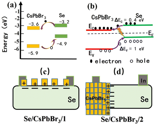
For CsPbBr3, the positions of the conduction band minimum (CBM) and valence band maximum (VBM) respectively are located at −3.6 eV and −5.9 eV relative to the vacuum energy level (0 eV) and the corresponding band gaps are 2.3 eV.30,33 Also, for Se with a bandgap of 1.7 eV, the CBM and VBM positions are relatively at −3.2 eV and −4.9 eV.34,35 Thus, the band alignment of the Se and CsPbBr3 is displayed in Fig. 6a. To gain more insight into the mechanism of the self-powered Se/CsPbBr3 PDs, the built-in electric field formed at the interface between p-Se and CsPbBr3 and the energy band diagram of the Se/CsPbBr3 heterojunction is sketchily plotted in Fig. 6b. The simplified structures of the two devices are illustrated in Fig. 6c and d. For the self-powered features of the two devices, the heterojunction is formed between the p-type Se wire and n-type CsPbBr3 particles interface. As shown in Fig. 6b, under light illumination, photo-generated electrons and holes will be quickly separated by the built-in electric field. The transfer of electron and holes will empower the PD to work without external bias. Due to the excellent intrinsic physical properties of Se and CsPbBr3, both the two structures of Se/CsPbBr3 heterojunction have high photocurrents (in nA), fast response speed and large on/off ratio under the bias of 0 V. Furthermore, both the two devices display broadband response from UV to visible light range because of the narrow bandgap of Se. Therefore, the Se wire is the primary carrier transport channel, and the build-in electric field provides the driving force. The Se/CsPbBr3/2 is a typical type-II heterojunction, which brings about a stronger built-in electric field and then achieving a larger open-circuit voltage (0.9 V), promoting more electron–hole pairs separation under light irradiation. The open circuit voltage increases logarithmically with the increase of the incident light intensity,36 but its maximum value does not exceed the built-in voltage. The inhomogeneous distribution of CsPbBr3 particles on the surface of Se wire produces a smaller open-circuit voltage of 0.1 V for the Se/CsPbBr3/1 device. For the responsivities of the devices, CsPbBr3 is excited under around 550 nm (the PL profiles of CsPbBr3 particle is shown in Fig. S1†), the holes of Se wire mainly contribute to the photocurrent which will be weakened by the depletion region, thus the responsivities of the Se/CsPbBr3/1 PD have a valley at about 550 nm. The Se/CsPbBr3/1 device can be considered as a parallel circuit between Se and CsPbBr3, and the Se/CsPbBr3/2 device is similar to a series circuit between Se and CsPbBr3. In addition to working at zero bias, the theoretical equivalent circuit promises the device working at different biases to achieve multifunction operation, as observed the binary response in Fig. 5. For the Se/CsPbBr3/2 device, the dark current is at a relatively high level at the bias of −0.9 V while the photocurrent goes down to the lowest point. This phenomenon provides an additional pathway to remove the negative effect of the noise signal and might fulfill the demand of weak-signal detection.37
3. Conclusion
In summary, ultralong Se wires have been synthesized via chemical vapor deposition, and the PDs based on single Se wire and CsPbBr3 particles with different heterostructures have been developed. For Se/CsPbBr3/1 PDs, CsPbBr3 particles are decorated on the surface of the Se wire, while for Se/CsPbBr3/2 heterojunction, it covers only half of the Se wire. Due to the built-in field formed between Se and CsPbBr3, both devices present self-powered, broad spectrum response (UV–visible), fast response speed (a rise time approaching μs magnitude), as well as the interesting binary response. The different device architectures yield different built-in electric field distributions. A stronger built-in electric field is confirmed from the significantly larger open-circuit voltage of 0.9 V for Se/CsPbBr3/2 PDs compared to 0.1 V for Se/CsPbBr3/2 PDs. Moreover, the responsivity and detectivity of Se/CsPbBr3/2 device show a quick rise at around 550 nm, whereas the Se/CsPbBr3/1 device present a valley at around 550 nm. These results demonstrate that the PD performance is closely dependent on the distribution of the built-in electric field within the heterostructures, which provides guidance for designing tunable, self-powered PDs for practical applications.4. Experiment section
4.1 Synthesis of Se wires
Se wires were synthetized in a horizontal tube furnace via typical vapor deposition method. Se source (>99.95%, Aladdin) was in the center of the furnace and silicon wafer was placed downstream from Se source vertically. Before heating, nitrogen (N2, >99.999%) was flushed at rate of 300 standard cubic center meter (sccm) for about 30 min to remove the remaining air. Subsequently, the tube furnace was quickly heated to 300 °C and was maintained for 10 hours under the protective gas of nitrogen. The temperature of the silicon wafer was about 150 °C during the transport and growth process. Then the tube furnace naturally cooled down to room temperature and a lot of Se wires are achieved. The length of the Se wires reaches centimeter scale, and these wires can be easily transferred and fabricated into devices.4.2 Fabrication of Se/CsPbBr3 heterojunctions
All the chemicals were purchased from Aladdin. To prepare CsPbBr3 solution, 0.45 M CsBr (99.9%) and 0.45 M PbBr2 (99.999%) were dissolved in dimethyl sulfoxide (DMSO, 99.9%) solution. The solution was stirred on a hot plate until it was completely dissolved and further filtered by using a syringe filter (0.22 μm). Single Se wire was transferred to the glass substrate. The Se/CsPbBr3/1 structure was formed by dropping the CsPbBr3 solution onto the whole Se wire which was placed on a glass substrate. To obtain the Se/CsPbBr3/2 structure, the CsPbBr3 solution was dropped onto half of the Se wire which was placed on two separated glass substrate. Then these Se/CsPbBr3 composites were heated it up to 60 °C for 30 min in ambient conditions. For both devices, two small pieces of indium pastes were doctoral-bladed onto the composites as electrodes to construct PDs. Our devices were both prepared based on Se wires. Consequently, the area of the device is roughly estimated to be 2.40 × 10⁻⁸ m2 according to the size of the Se wire (12 μm × 2 mm).4.3 Material characterization
A Field-Emission Scanning Electron Microscopy (FE-SEM, Zeiss Sigma) were used to characterize sample morphologies. X-ray diffraction (XRD) patterns were collected on a Bruker D8-A25 diffractometer using Cu Kα radiation (λ = 1.5405 Å) in the 2θ range from 10° to 80°. X-ray photoelectron spectroscopy (XPS, PerkinElmer PHI 5000C ESCA system equipped with a hemispherical electron energy analyzer) was experimentally utilized to investigate the composition and chemical state of the samples. The binding energy for C 1s peak at 285 eV was used as the reference for calibration. The photoelectric performance was characterized with a program-controlled semiconductor characterization system (Keithley 4200, USA). Time resolved responses of the device were measured with YAG:Nd laser with pulse duration of 3–5 ns (Continuum Electro-Optics, MINILITE II, 355 nm), oscilloscope (Tektronix MSO/DPO5000), and a 1 GΩ resistor. The light intensity was measured with a NOVA II power meter (OPHIR Photonics). The intensity of the light source used is related to the wavelength, and the corresponding wavelength will be used to calculate the responsivity, and the light intensity as shown in the Fig. S2.† All the measurements were performed at the room temperature.Author contributions
Jiaojiao Liu: investigation, experimentalize, data curation, visualization, writing – original draft. funding acquisition. Jie Zhang: writing – review & editing, supervision, project administration, funding acquisition.Conflicts of interest
The authors declare no conflict of interest.Acknowledgements
This work was financially supported by the National Natural Science Foundation of China (Grant No. 11904034) and the Natural Science Foundation of Jiangsu Province of China (Grant No. BK20191025). Zhang Jie acknowledged the support of the National Natural Science Foundation of China (Grant No. 61704012).References
- D. Periyanagounder, T. C. Wei, T. Y. Li, C. H. Lin, T. P. Goncalves, H. C. Fu, D. S. Tsai, J. J. Ke, H. W. Kuo, K. W. Huang, N. Lu, X. S. Fang and J. H. He, Adv. Mater., 2020, 32, 1904634 CrossRef CAS PubMed.
- J. X. Chen, W. X. Ouyang, W. Yang, J. H. He and X. S. Fang, Adv. Funct. Mater., 2020, 30, 1909909 CrossRef CAS.
- X. Y. Zhao, L. X. Huang, Y. K. Wang, X. L. Zhua, L. Li, G. X. Li and W. H. Sun, RSC Adv., 2020, 10, 32976 RSC.
- C. Q. Zhou, K. W. Liu, X. Chen, J. H. Feng, J. L. Yang, Z. Z. Zhang, L. Liu, Y. Xia and D. Z. Shen, J. Alloys Compd., 2020, 840, 155585 CrossRef CAS.
- Z. He, J. Guo, S. Li, Z. Lei, L. Lin, Y. Ke, W. Jie, T. Gong, Y. Lin, T. Cheng, W. Huang and X. Zhang, Adv. Mater. Interfaces, 2020, 7, 2070050 CrossRef.
- Y. Zhang, F. Cao, S. Y. Li, X. Y. Liu, L. X. Kang, L. M. Wu and X. S. Fang, J. Mater. Sci. Technol., 2022, 129, 108 CrossRef.
- Y. Zhang, W. L. Liu, Y. S. Liu, C. H. Wang, G. D. Zhu and W. D. Song, J. Mater. Chem. C, 2021, 9, 15654 RSC.
- W. Zhu, M. Deng, D. Chen, Z. Zhang, W. Chai, D. Chen, H. Xi, J. Zhang, C. Zhang and Y. Hao, ACS Appl. Mater. Interfaces, 2020, 12, 32961 CrossRef CAS PubMed.
- Y. Zheng, Y. Li, X. Tang, W. Wang and G. Li, Adv. Opt. Mater., 2020, 8, 2000197 CrossRef CAS.
- K. Shen, H. Xu, X. Li, J. Guo, S. Sathasivam, M. Wang, A. Ren, K. Choy, I. Parkin, Z. Guo and J. Wu, Adv. Mater., 2020, 32, 2000004 CrossRef CAS PubMed.
- Y. Zhang and W. D. Song, J. Mater. Chem. C, 2021, 9, 4799 RSC.
- B. Ouyang, C. Chang, L. Zhao, Z. Wang and Y. Yang, Nano Energy, 2019, 66, 104111 CrossRef CAS.
- H. J. Fang, C. Zheng, L. L. Wu, Y. Li, J. Cai, M. X. Hu, X. S. Fang, R. Ma, Q. Wang and H. Wang, Adv. Funct. Mater., 2019, 29, 1809013 CrossRef.
- L. Luo, X. Yang, F. Liang, J. Jie, Q. Li, Z. Zhu, C. Wu, Y. Yu and L. Wang, CrystEngComm, 2012, 14, 1942 RSC.
- B. Gates, B. Mayers, B. Cattle and Y. Xia, Adv. Funct. Mater., 2002, 12, 219 CrossRef CAS.
- M. Tomoaki, S. Ichitaro, Y. Takatoshi, O. Masanori, Y. Hisato, S. Yu, O. Kousuke, K. Nanako, O. Shuichi and T. Yuji, Sensors, 2013, 13, 13744 CrossRef PubMed.
- J. Qin, G. Qiu, W. He, J. Jian, M. Si, Y. Duan, A. Charnas, D. Zemlyanov, H. Wang, W. Shao, L. Zhen, C. Xu and P. Ye, Adv. Funct. Mater., 2018, 28, 1806254 CrossRef.
- K. Hu, F. Teng, L. X. Zheng, P. P. Yu, Z. M. Zhang, H. Y. Chen and X. S. Fang, Laser Photonics Rev., 2017, 11, 1600257 CrossRef.
- K. Hu, H. Y. Chen, M. Jiang, F. Teng, L. X. Zheng and X. S. Fang, Adv. Funct. Mater., 2016, 26, 6641 CrossRef CAS.
- P. Yu, K. Hu, H. Chen, L. Zheng and X. Fang, Adv. Funct. Mater., 2017, 27, 1703166 CrossRef.
- J. Qin, G. Qiu, J. Jian, H. Zhou, L. Yang, A. Charnas, D. Zemlyanov, C. Xu, X. Xu, W. Wu, H. Wang and P. Ye, ACS Nano, 2017, 11, 10222 CrossRef CAS PubMed.
- C. L. Li, Y. Ma, Y. F. Xiao, L. Shen and L. M. Ding, InfoMat, 2020, 2, 1247 CrossRef CAS.
- L. Li, H. Y. Chen, Z. M. Fang, X. Y. Meng, C. T. Zuo, M. L. Lv, Y. Z. Tian, Y. Fang, Z. Xiao, C. X. Shan, Z. G. Xiao, Z. W. Jin, G. Z. Shen, L. Shen and L. M. Ding, Adv. Mater., 2020, 32, 1907257 CrossRef CAS PubMed.
- L. Protesescu, S. Yakunin, M. Bodnarchuk, F. Krieg, R. Caputo, C. Hendon, R. Yang, A. Walsh and M. Kovalenko, Nano Lett., 2015, 15, 3692 CrossRef CAS PubMed.
- L. Lv, Y. Xu, H. Fang, W. Luo, F. Xu, L. Liu, B. Wang, X. Zhang, D. Yang and W. Hu, Nanoscale, 2016, 8, 13589 RSC.
- X. Jia, C. Zuo, S. Tao, K. Sun, Y. Zhao, S. Yang, M. Cheng, M. Wang, Y. Yuan, J. L. Yang, F. Gao, G. C. Xing, Z. Wei, L. Zhang, H. L. Yip, M. Liu, Q. Shen, L. Yin, L. Han, S. Liu, L. Wang, J. Luo, H. Tan, Z. Jin and L. Ding, Sci. Bull., 2019, 64, 1532 CrossRef CAS.
- Y. Shen, C. Wei, L. Ma, S. Wang, X. Wang, X. Xu and H. Zeng, J. Mater. Chem. C, 2018, 6, 12164 RSC.
- L. Zhou, K. Yu, F. Yang, H. Cong, N. Wang, J. Zheng, Y. Zuo, C. Li, B. Cheng and Q. Wang, J. Mater. Chem. C, 2017, 5, 6224 RSC.
- Y. Zhang, W. Xu, X. Xu, J. Cai, W. Yang and X. Fang, J. Phys. Chem. Lett., 2019, 10, 836 CrossRef CAS PubMed.
- M. N. Xue, H. Zhou, G. K. Ma, L. Yang, Z. H. Song, J. Zhang and H. Wang, Sol. Energy Mater. Sol. Cells, 2018, 187, 69 CrossRef CAS.
- Y. Li, Y. Zhang, Z. Chen, Q. Li, T. Li, M. Li, H. Zhao, Q. Sheng, W. Shi and J. Yao, Photonics Res., 2020, 8, 1301 CrossRef.
- Y. Zhang, S. Y. Li, W. Yang, M. K. Joshi and X. S. Fang, J. Phys. Chem. Lett., 2019, 10, 2400 CrossRef CAS PubMed.
- X. Y. Liu, X. H. Tan, Z. Y. Liu, X. N. Zhang, T. L. Shi and G. L. Liao, J. Mater. Chem. C, 2020, 8, 14409 RSC.
- S. Joshi and C. Lokhande, Appl. Surf. Sci., 2006, 252, 8539 CrossRef CAS.
- W. Yang, K. Hu, F. Teng, J. H. Weng, Y. Zhang and X. S. Fang, Nano Lett., 2018, 18, 4697 CrossRef CAS PubMed.
- G. Yu, L. P. Dong, B. Peng, L. Yuan, Y. Huang, L. C. Zhang, Y. M. Zhang and R. X. Jia, J. Alloys Compd., 2020, 821, 153532 CrossRef.
- Q. Hong, Y. Cao, J. Xu, H. Lu, J. He and J. Sun, ACS Appl. Mater. Interfaces, 2014, 6, 20887 CrossRef CAS PubMed.
Footnote |
| † Electronic supplementary information (ESI) available. See DOI: https://doi.org/10.1039/d2ra06597e |
| This journal is © The Royal Society of Chemistry 2022 |

