 Open Access Article
Molecular planting of a single organothiol into a “gap-site” of a 2D patterned adlayer in an electrochemical environment†
Soichiro
Yoshimoto
 *a and
Hiroto
Ogata
b
aInstitute of Industrial Nanomaterials, Kumamoto University, 2-39-1 Kurokami, Chuo-ku, Kumamoto 860-8555, Japan. E-mail: so-yoshi@kumamoto-u.ac.jp
bGraduate School of Science and Technology, Kumamoto University, 2-39-1 Kurokami, Chuo-ku, Kumamoto 860-8555, Japan
First published on 8th April 2022
Abstract
The self-assembled inclusion of molecules into two-dimensional (2D) porous networks on surfaces has been extensively studied because 2D functional materials consisting of organic molecules have become an important research topic. However, the isolation of a single molecular thiol remains a challenging goal. Here, we report a method of planting and isolating organothiols onto a 2D patterned organic adlayer at an electrochemical interface. In situ scanning tunneling microscopy revealed that the phase transition of an ovalene adlayer is electrochemically induced and that the gap site created by three ovalene molecules serves as a 2D molecular template to isolate thiol molecules and to standardize the distance between them via the formation of precise selective open spaces, suggesting that electrochemical “molecular planting” opens applications for 2D patterns of isolated single organothiol molecules.
Introduction
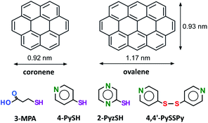
The appearance and control of function are important for the construction of new nanoarchitectures1–3 and for precise molecular recognition.4,5 Recently, an innovative molecular design and synthesis approach based on coordination chemistry and supramolecular chemistry has been proposed.6–11 The construction of supramolecular assembly based two-dimensional (2D) nanoarchitectures has also been explored in the field of nanoscale surface science as a method of controlling the surface properties,12–18 especially by means of scanning tunneling microscopy (STM). Many studies on bicomponents consisting of functional molecules and/or on the coadsorption of functional molecules with solvents have been recognized in the field of surface science.13,14,19–26 Since the early 1980s,27,28 self-assembled monolayers (SAMs) have been widely recognized; they are formed via a simple method of preparing organic monolayers on metal surfaces such as Au, Ag, and Cu, especially to develop functional electrodes modified with thiols or thiols and sensors, metal nanoclusters, and functionality for molecular recognition of biomaterials and for lithography.27–40 SAMs have been used as a platform to create controlled nanospaces, the so-called surface-supported metal–organic frameworks,38,39via layer-by-layer coordination on functionalized surfaces.39 In contrast, the formation of the melamine (ML)–perylenetetracarboxylic diimide (PTCDI) network is important in the fields of surface science and supramolecular chemistry because the network is highly stable due to the formation of hydrogen bonds at three points; this network arrangement enables the further inclusion of not only C60 molecules41,42 but also thiols in the cavities.43 Buck's group subsequently reported that an identical honeycomb array can also be prepared from the solution phase.43,44 Several thiols were trapped in cavities consisting of ML-PTCDI, demonstrating that this three-point hydrogen bonding is much stronger than normal hydrogen bonding between two carboxylic acid groups; their reports were also followed by theoretical calculations.45 A periodically isolated, not self-assembled monolayer of thiolates is expected to enable not only an understanding of fundamental properties such as molecular tilt angle and rotation but also molecular nanopatterning and precise molecular interactions. However, the formation of a single isolated thiolate monolayer has not yet been successfully demonstrated, thus representing a challenge in the surface engineering field. In general, since the combination of physisorption and chemisorption often causes phase separation in the adlayer, the isolation of thiol molecules bonded to Au atoms is extremely difficult with coadsorption due to the adsorption equilibrium in organic solvents. It is necessary to fabricate gaps and/or vacancies at the surface to adsorb a single thiol molecule. Thus, creating an adsorption site for a single thiol molecule remains a challenge. From the standpoint of electrochemical surface science, an in situ STM study combined with electrochemistry (EC) can provide detailed nanoscale information about the structural changes in both the physisorbed organic adlayer21–23,46–48 and the chemisorbed layers via the electrode potential.49–53 The advantage of EC conditions is the ability to control the surface charge by changing the electrode potential.46 For example, the adlayer structure and/or phase transition of SAMs can be tuned by the electrode potentials in electrolyte solutions.50–53 We have investigated 2D adlayers of polycyclic aromatic hydrocarbons (PAHs), such as coronene, and larger compounds. As reported in our previous works, coronene forms a highly ordered adlayer on Au(111) and is stable at the electrochemical interface in aqueous electrolyte solutions due to its low solubility in water.54,55 Subsequently, coadsorption of coronene and organic solvents on Au(111) was reported by the Hipps group.25,26 Recently, we succeeded in preparing a water-insoluble PAH adlayer composed of dicoronylene on Au(111) using water-soluble molecular capsules consisting of bent-type anthracene amphiphilic molecules, the so-called “molecular container” approach.56 The formation of a highly ordered adlayer of PAHs incorporated with Cl− and Br− suggests that PAH adlayers stabilize thiol adsorption in the “gap” site.56,57 It is important to understand the relationship between the thiolate S atom and the interacting site on the Au surface. Such nanoscale information provides details on the self-assembly of thiols on the surface.Here, we propose an approach to the patterned and isolated adsorption of thiol onto surface-supported characteristic nanostructures of ovalene at an electrochemical interface (see Chart 1). The specially arranged ovalene adlayer on a Au(111) electrode surface can accept a single thiol in the nanocavity.
Results and discussion
Electrochemical structural change of the ovalene adlayer
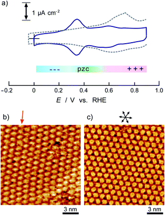
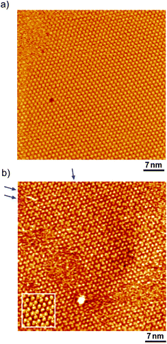
Fig. 1 shows a typical cyclic voltammogram of the ovalene-modified Au(111) electrode in the electric double-layer potential region. A small redox couple is clearly observed at +0.33 V. The electronic charge consumed by the reductive peak area was calculated to be 0.25 ± 0.10 μC cm−2, indicating that this transferred charge is not associated with the redox reaction (faradaic current) of ovalene molecules. Rather, it is associated with a phase transition involving a weak charge transfer reaction in which the adlayer undergoes on the Au(111) surface. In general, the potential of zero charge (pzc) for a Au(111) electrode in HClO4 is 0.23 V vs. SCE.58 This value is calibrated to be 0.47 V vs. RHE. Since ovalene has a π-electron system, π-electrons are donated from each ovalene molecule to the Au(111) surface. Potential manipulation in the case of potentials more negative than the pzc causes electrostatic repulsion between the ovalene adlayer and the Au(111) surface. After the CV profiles were confirmed, in situ STM measurements were performed in 0.1 M HClO4. First, an STM image of an ovalene adlayer on Au(111) was obtained at an open-circuit potential (OCP) of approximately 0.80 V. Details of the internal structure, molecular orientation and packing arrangement are evident in the high-resolution STM image in Fig. 1b, which shows that the micro-orientation of ovalene on Au(111) is random. Indeed, it seems to distort molecular rows, especially in the y-direction in the STM image. The intermolecular distance between the centers of the ovalene molecules was measured to be approximately 1.5 nm, whereas the average distance in the y-direction indicated by the red arrow was shorter, 1.1–1.2 nm (the cross-sectional profiles are displayed in ESI, Fig. S1†). This shorter distance is not due to the thermal drift during the scan but the low-symmetry structure of ovalene. In contrast, a structural change was observed in the ovalene adlayer when the potential was maintained at potentials more negative than 0.25 V. Fig. 1c shows the completely different pattern that appeared in the STM image immediately after the potential was decreased to 0.25 V from 0.75 V vs. RHE, revealing a long-range-ordered ovalene adlayer with a characteristic molecular arrangement. Fig. 1c clearly shows that the close-packed Au atomic rows, which are marked by the set of three arrows in the figure, match the corresponding molecular rows of ovalene. Furthermore, the molecular rows parallel to the directions of the substrate are indicated by the arrows. In addition, the STM image allowed us to determine the internal structure and orientation of each ovalene molecule. The elongated features along the longer molecular axis were discerned for each molecule. Additionally, individual molecules clearly exhibited an oval shape, as expected from the molecular model. The ovalene molecules were perfectly aligned, with a regular micro-orientation along the molecular rows. Periodic rotation of the ovalene molecules by 60° was observed within each molecular row, with every third molecule being oriented in the same orientation. The average nearest-neighbor distance of 1.22 nm is equivalent to 4 times the Au lattice spacing of 0.288 nm. A similar STM image was previously obtained for a naphthalene adlayer on a Rh(111) electrode surface.59 The molecular symmetry of PAHs plays an important role in the formation of the characteristic molecular arrangement, especially in the electrochemical phase transition in the ovalene molecular adlayer. From another viewpoint, if a triangular vacancy site can be found, the obtained structure can be considered a triangle-shaped formation consisting of three ovalene molecules in an arrangement similar to a rice ball. The phase transition under controlled potential was thus a transition to a metastable adlayer on Au(111). Indeed, according to density functional theory (DFT) calculations for PAH molecules and a Au surface, charge transfer occurs from the Au surface to the PAH molecules,60 suggesting that the surface charge density can be precisely modulated by the applied potential at the electrochemical interface and appears to contribute not only to the molecule–substrate interaction but also to the interactions among the molecules. PAHs are generally neutral, but they have π electrons. Therefore, ovalene is considered to be slightly negative. Although we cannot quantitatively estimate the charge transfer under the present conditions, the electrode potential manipulation in the negative direction repulsively causes π electron donation from the ovalene molecules to the Au surface and relaxation in the adlayer due to the resulting structural change. Thus, the low symmetry of the ovalene molecule contributes to the formation of a characteristic nanopattern.After the structural change of the ovalene adlayer on Au(111) was confirmed, the selective adsorption of several thiols was investigated at the potential. A large-scale STM image of the ovalene adlayer on Au(111) obtained at 0.25 V is shown in Fig. 2a. In the scanning area, despite the presence of several defects, a single domain with a uniform arrangement of ovalene molecules was formed on the terraces. After the observation of the structural change in the ovalene adlayer, a droplet of 10 μM 3-MPA aqueous solution was carefully added into the EC-STM cell at 0.22 V vs. RHE (final concentration in the cell was less than approximately 0.1 μM). After more than 20 min, several bright spots began to appear at a central dark gap site consisting of three ovalene molecules, as shown in Fig. 2b. With increasing time, 3-MPA molecules were adsorbed at a high density into the ovalene adlayer gap-site. Even in the large scan area, characteristic triangles arranged in a clover shape can be observed. In particular, many central spots were contained in the molecular rows indicated by the blue arrows, as shown in the inset of a high-resolution STM image. The surface was gradually replaced with 3-MPA molecules if a higher concentration of 3-MPA, such as 50 μM aqueous solution, was added into the cell (see Fig. S3†). To compare the effect of the structure on the underlying PAH adlayer, we also investigated the coronene adlayer on Au(111) in the presence of 3-MPA. When a coronene adlayer, which forms highly ordered and hexagonally arranged arrays, was used in the same manner, no characteristic change was observed at 0.25 V because the coronene molecules formed a closely packed, (4 × 4) adlayer structure on Au(111)54 (see Fig. S4†). These results indicate that the gap site surrounded by coronene molecules was smaller than that formed by ovalene molecules induced by the potential manipulation. However, the replacement reaction with 3-MPA easily occurred when the potential was adjusted to 0.60 V vs. RHE (see also Fig. S5†), as previously reported in the literature.50 The electrode potential plays a significant role in the adsorption–desorption equilibrium between the thiol solution phase and Au(111) electrode surface.
Selective adsorption of thiols into the open space of the ovalene adlayer
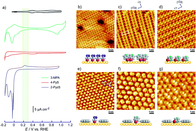
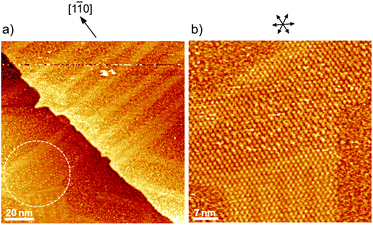
To understand the stability of individual thiols on Au(111), the electrochemical behaviors of each SAM on Au(111) were investigated in 0.05 M HClO4. From the CV profiles of each SAM on Au(111) obtained in 0.05 M HClO4 (Fig. 3a), we can understand the strength of SAM on Au(111). As reported in the previous literature, the reductive desorption of 3-MPA-SAM takes place at potentials more negative than 0.2 V vs. RHE,49 whereas 4-PyS-SAM revealed several phase transitions.51 2-PyzS molecules reductively desorbed from the Au(111) surface at potentials more negative than 0 V. Although the voltammetric shape is complicated (for example, several sharp reductive peaks were observed in the potential region between 0 and –0.2 V), no current was seen from 0.9 to 0.1 V. In the case of 2-PyzS-SAM, the 2-PyzS molecule can adsorb not only thiol S atoms but also N atoms because the 2-PyzS molecule contains two N atoms. Therefore, it is considered that the interaction between the molecule and Au substrate is stronger than those of the 3-MPA and 4-PyS molecules. Based on the voltammetric results, the adsorption–desorption equilibrium of thiols can be controlled in the potential range from 0.30 to 0.05 V with precise potential manipulation because the potential region is the exclusive condition to trigger the reductive desorption of SAM at the electrochemical interface. To understand the adsorption at the gap site consisting of the ovalene adlayer, the formation of characteristic triangles was compared with individual SAMs in the high-resolution STM images. As shown in Fig. 3b–d, highly ordered structures with commensurate 3 × 3, p(5 × √3 R−30°), and p(5 × √7 R−40.9°) adlattices were formed for 3-MPA,49 4-PyS,51,61,62 and 2-PyzS-SAMs,63 respectively. In particular, the individual Py moieties of 4-PyS-SAM were observed in molecular rows with a dimer form. In the STM image, it seems that two pyridine rings are resolved with three spots for each Py ring and oriented in the same direction. In the case of 2-PyzS-SAM, a single 2-PyzS molecule is assigned to the two spots. When the distance is considered, the two spots correspond to the thiolate S and pyrazine N atoms. This assignment is supported by the results reported for the 2-pyridinethiolate SAM64 as well as by those reported for other SAMs containing S and N atoms.65,66 In contrast to SAMs, the central parts of each gap site consisting of ovalene molecules are filled with a bright spot and exhibit a three-leaf clover shape for 3-MPA in the ovalene adlayer (blue lines superimposed in Fig. 3e). The distance between the centers was approximately 2.2 nm, which is almost identical to the size of the gap site surrounded by three ovalene molecules in the absence of 3-MPA. On the basis of the high-resolution STM image, we deduced that each bright spot corresponds exactly to the location of the gap site. In the case of 4-PyS, several bright spots also appeared at a central dark gap site consisting of three ovalene molecules, as shown in Fig. 3f. A comparison of the two STM images shown in Fig. 3c and f reveals that the size of the bright spot was obviously smaller than the 4-Py ring shown in Fig. 3c. According to the DFT calculations of the adsorption site of the 4-PyS isolated on a Au(111) lattice,67 the pyridine ring of 4-PyS adsorbed onto Au(111) was estimated to tilt by 35° with respect to the perpendicular direction. Therefore, the bright spot surrounded by three ovalene molecules was appropriately assigned to the thiolate S atom. Under the experimental conditions, we observed several bright spots in the “gap site” consisting of ovalene molecules, although PyS− was considered to adsorb preferentially on bare Au sites created by three ovalene molecules. During at least 20 min of observation, the number of bright spots did not increase, and the spot position did not change, indicating that the spot corresponded exactly to the S atom chemically bonded to the Au surface. To further extend our knowledge, bis(4-pyridyl)disulfide (4,4′-PySSPy), which is the dimer of 4-PySH, was also examined on the ovalene adlayer (see Fig. S6†). Interestingly, identical structures were observed at the gap site surrounded by three ovalene molecules, indicating that PySSPy cleaved to two pyridinethiolates (PyS−); i.e., the bond between PyS and Au formed not on the surface but rather through PyS− in acidic solution. This result elucidates the adsorption of self-assembled monolayers onto Au. In contrast, each 2-PyzS molecule in the ovalene adlayer yielded an image with two bright protrusions, not a single spot, as shown in Fig. 3g. The distance between the two spots was approximately 2.7 Å, corresponding to the distance between the S and N atoms in 2-PyzSH (Chem3D model structure). The two bright spots in each cavity were approximately aligned in the [1![[1 with combining macron]](https://www.rsc.org/images/entities/char_0031_0304.gif) 0] direction. Additionally, the two bright spots were positioned in the cavity rather than in a central position. This electronic feature strongly suggests that 2-PyzS adsorption to the Au surface is accomplished through thiolate S and pyrazine N atoms. The presence of this feature also supports the hypothesis that a chemical bond formed between the thiolate S atom and Au substrate rather than thiolate S attachment via physisorption. Indeed, in a relatively large area (Fig. 4a), a highly ordered array of ovalene molecules was observed on a surface containing partially reconstructed rows. As shown in Fig. 4b, a careful inspection of the corresponding large-scale STM image (the area surrounded by the dotted circle in Fig. 4a) revealed that 2-PyzS molecules adsorbed into the gap-site consisting of an ovalene adlayer in the region of unreconstructed (1 × 1), not on the reconstructed rows. The adsorption of thiols on the (1 × 1) region strongly resembles chemisorption. A larger aromatic thiol, 4′-mercapto-2,2′:6′,2′′-terpyridine (4′-terPySH), was also examined on the ovalene adlayer to obtain detailed information on the structural differences. In the case of 4′-terPySH, no change in the STM image was observed under the same modification conditions. Selective adsorption into the gap site consisting of an ovalene adlayer is difficult because 4′-terPySH is poorly soluble in water. Based on these results, the amounts of thiols entrapped in the cavities depend on the chemical structure of the thiol. Although the percentage of entrapped thiols is determined by the domain size of the ovalene adlayer, 3-MPA molecules were more easily trapped in the cavities than 4-PySH. From the STM image shown in Fig. 2b, 3-MPA can be roughly estimated to occupy 40∼50% of the cavities. In contrast, 4-PySH occupied less than 10%, whereas 2-PyzH molecules entrapped approximately 30% of the cavities. The entrapment of thiols can be tentatively explained by the difference in pKa of thiol and/or the thione formation, especially 4-PySH, because of tautomerization.
0] direction. Additionally, the two bright spots were positioned in the cavity rather than in a central position. This electronic feature strongly suggests that 2-PyzS adsorption to the Au surface is accomplished through thiolate S and pyrazine N atoms. The presence of this feature also supports the hypothesis that a chemical bond formed between the thiolate S atom and Au substrate rather than thiolate S attachment via physisorption. Indeed, in a relatively large area (Fig. 4a), a highly ordered array of ovalene molecules was observed on a surface containing partially reconstructed rows. As shown in Fig. 4b, a careful inspection of the corresponding large-scale STM image (the area surrounded by the dotted circle in Fig. 4a) revealed that 2-PyzS molecules adsorbed into the gap-site consisting of an ovalene adlayer in the region of unreconstructed (1 × 1), not on the reconstructed rows. The adsorption of thiols on the (1 × 1) region strongly resembles chemisorption. A larger aromatic thiol, 4′-mercapto-2,2′:6′,2′′-terpyridine (4′-terPySH), was also examined on the ovalene adlayer to obtain detailed information on the structural differences. In the case of 4′-terPySH, no change in the STM image was observed under the same modification conditions. Selective adsorption into the gap site consisting of an ovalene adlayer is difficult because 4′-terPySH is poorly soluble in water. Based on these results, the amounts of thiols entrapped in the cavities depend on the chemical structure of the thiol. Although the percentage of entrapped thiols is determined by the domain size of the ovalene adlayer, 3-MPA molecules were more easily trapped in the cavities than 4-PySH. From the STM image shown in Fig. 2b, 3-MPA can be roughly estimated to occupy 40∼50% of the cavities. In contrast, 4-PySH occupied less than 10%, whereas 2-PyzH molecules entrapped approximately 30% of the cavities. The entrapment of thiols can be tentatively explained by the difference in pKa of thiol and/or the thione formation, especially 4-PySH, because of tautomerization.
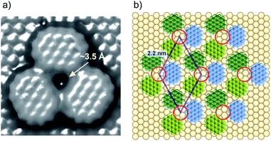
Taking a simple adlayer structure formed with three ovalene molecules into consideration, the gap site was estimated by molecular mechanical (MM) calculations. Based on the MM calculation shown in Fig. 5a, the gap site consisting of three ovalene molecules can accept a thiolate with a diameter of approximately 3 Å. A structural model of thiolates in an electrochemically induced ovalene adlayer is proposed in Fig. 5b. STM images show that molecular rows of ovalene in the adlayer are almost aligned with the lattice directions. The lattice, consisting of vacancies, is superimposed with a rhombus. If the triangular gap site is periodically repeated with a distance of 2.2 nm, the center of the gap site is located at either the threefold hollow or near twofold bridge site of the Au lattice, as indicated by red circles, because the distance between gap sites is an incommensurate for the Au atomic lattice structure. Therefore, thiol adsorption is site-selective. In contrast, the central position of each ovalene molecule is located preferentially at the bridge site. According to a recent theoretical calculation, PAHs such as hexabenzocoronene adsorb onto the bridge site rather than the top site of the Au atoms in Au12 clusters.60
Conclusions
We demonstrated the formation of regularly patterned hybrid adlayers at an electrified solid–liquid interface. Water-soluble thiols were successfully isolated via the electrochemically induced phase transition of the ovalene adlayer at an electrochemical interface of Au(111) in an electrolyte aqueous solution. The potential switching to 0.25 V plays an important role not only in controlling the charge distribution from the Au surface to the ovalene molecule but also in controlling the equilibrium between the adsorption and desorption of thiols at the Au(111) electrode surface. Thus, the electrochemically produced ovalene adlayer on the Au(111) electrode surface can serve as a molecular template for special patterning of several thiols.Data availability
Several supporting data have been uploaded as ESI.†Author contributions
SY: conceptualization; methodology; EC-STM investigation; data curation; funding acquisition; project administration; supervision; writing – review & editing. HO: EC-STM investigation; data curation; writing – original draft. All authors discussed the results and commented on the manuscript.Conflicts of interest
There are no conflicts to declare.Acknowledgements
This work was supported by JSPS KAKENHI [grant number 19H02560], the Sumitomo Foundation and the IINa Interdisciplinary Research Project of the Institute of Industrial Nanomaterials, Kumamoto University. MM calculations were supported by the “Nanotechnology Platform Japan (NTPJ)” projected by the Minister of Education, Culture, Sports, Science and Technology (MEXT) at Kyushu University.Notes and references
- D. S. Su, S. Perathoner and G. Centi, Chem. Rev., 2013, 113, 5782–5816 CrossRef CAS PubMed.
- X.-S. Xu, K. Müllen and A. Narita, Bull. Chem. Soc. Jpn., 2020, 93, 490–506 CrossRef CAS.
- K. Ariga and M. Shionoya, Bull. Chem. Soc. Jpn., 2021, 94, 839–859 CrossRef CAS.
- S. Durot, J. Taesch and V. Heitz, Chem. Rev., 2014, 114, 8542–8578 CrossRef CAS PubMed.
- M. Yoshizawa and L. Cotti, Acc. Chem. Res., 2019, 52, 2392–2404 CrossRef CAS PubMed.
- H. Takezawa and M. Fujita, Bull. Chem. Soc. Jpn., 2021, 94, 2351–2369 CrossRef CAS.
- H. Nishihara, K. Kanaizuka, Y. Nishimori and Y. Yamanoi, Coord. Chem. Rev., 2007, 251, 2674–2687 CrossRef CAS.
- H. Nishihara, Chem. Lett., 2014, 43, 388–395 CrossRef CAS.
- E. G. Percástegui, T. K. Ronson and J. R. Nitschke, Chem. Rev., 2020, 120, 13480–13544 CrossRef PubMed.
- T. Sawada and M. Fujita, Bull. Chem. Soc. Jpn., 2021, 94, 2342–2350 CrossRef CAS.
- T. Imaoka and K. Yamamoto, Bull. Chem. Soc. Jpn., 2019, 92, 941–948 CrossRef CAS.
- J. A. A. W. Elemans, I. De Cat, H. Xu and S. De Feyter, Chem. Soc. Rev., 2009, 38, 722–736 RSC.
- K. Tahara, S. Lei, J. Adisoejoso, S. De Feyter and Y. Tobe, Chem. Commun., 2010, 46, 8507–8525 RSC.
- S. Yoshimoto and K. Itaya, Annu. Rev. Anal. Chem., 2013, 6, 213–235 CrossRef CAS PubMed.
- F. L. Otte, S. Lemke, C. Schütt, N. R. Krekiehn, U. Jung, O. M. Magnussen and R. Herges, J. Am. Chem. Soc., 2014, 136, 11248–11251 CrossRef CAS PubMed.
- S. Mohnani and D. Bonifazi, Coord. Chem. Rev., 2010, 254, 2342–2362 CrossRef CAS.
- W. Auwärter, D. Écija, F. Klappenberger and J. V. Barth, Nat. Chem., 2015, 7, 105–120 CrossRef PubMed.
- J. M. Gottfreid, Surf. Sci. Rep., 2015, 70, 259–379 CrossRef.
- L. Dong, Z. Gao and N. Lin, Prog. Surf. Sci., 2016, 91, 101–135 CrossRef CAS.
- X. Bouju, C. Mattioli, G. Franc, A. Pujol and A. Gourdon, Chem. Rev., 2017, 117, 1407–1444 CrossRef CAS PubMed.
- S. Yoshimoto, N. Higa and K. Itaya, J. Am. Chem. Soc., 2004, 126, 8540–8545 CrossRef CAS PubMed.
- K. Suto, S. Yoshimoto and K. Itaya, Langmuir, 2006, 22, 10766–10776 CrossRef CAS PubMed.
- S. Yoshimoto, Y. Honda, O. Ito and K. Itaya, J. Am. Chem. Soc., 2008, 130, 1085–1092 CrossRef CAS PubMed.
- S. J. H. Griessl, M. Lackinger, F. Jamitzky, T. Markert, M. Hietschol and W. M. Heckl, J. Phys. Chem. B, 2004, 108, 11556–11560 CrossRef CAS.
- B. J. Gyarfas, B. Wiggins, M. Zosel and K. W. Hipps, Langmuir, 2005, 21, 919–923 CrossRef CAS PubMed.
- A. Jahanbekam, S. Vorpahl, U. Mazur and K. W. Hipps, J. Phys. Chem. C, 2013, 117, 2914–2919 CrossRef CAS.
- I. Taniguchi, K. Toyosawa, H. Yamaguchi and K. Yasukouchi, J. Chem. Soc., Chem. Commun., 1982, 1032–1033 RSC.
- R. G. Nuzzo and D. L. Allara, J. Am. Chem. Soc., 1983, 105, 4481–4483 CrossRef CAS.
- A. Ulman, Chem. Rev., 1996, 96, 1533–1554 CrossRef CAS PubMed.
- G. E. Poirier, Chem. Rev., 1997, 97, 1117–1127 CrossRef CAS PubMed.
- F. Schreiber, Prog. Surf. Sci., 2000, 65, 151–256 CrossRef CAS.
- R. K. Smith, P. A. Lewis and P. S. Weiss, Prog. Surf. Sci., 2004, 75, 1–68 CrossRef CAS.
- J. C. Love, L. A. Estroff, J. K. Kriebel, R. G. Nuzzo and G. M. Whitesides, Chem. Rev., 2005, 105, 1103–1169 CrossRef CAS PubMed.
- M. D. Porter, T. B. Bright, D. L. Allara and C. E. D. Chidsey, J. Am. Chem. Soc., 1987, 109, 3559–3568 CrossRef CAS.
- E. B. Troughton, C. D. Bain, G. M. Whitesides, R. G. Nuzzo, D. L. Allara and M. D. Porter, Langmuir, 1988, 4, 365–385 CrossRef CAS.
- C. E. D. Chidsey, C. R. Bertozzi, T. M. Putvinski and A. M. Mujsce, J. Am. Chem. Soc., 1990, 112, 4301–4306 CrossRef CAS.
- K. Uosaki, Y. Sato and H. Kita, Langmuir, 1991, 7, 1510–1514 CrossRef CAS.
- O. Shekhah, H. Wang, M. Paradinas, C. Ocal, B. Schüpbach, A. Terfort, D. Zacher, R. A. Fischer and C. Wöll, Nat. Mater., 2009, 8, 481–484 CrossRef CAS PubMed.
- M. Kind and C. Wöll, Prog. Surf. Sci., 2009, 84, 230–278 CrossRef CAS.
- T. Bürgi, Nanoscale, 2015, 7, 15553–15567 RSC.
- J. A. Theobald, N. S. Oxtoby, M. A. Phillips, N. R. Champness and P. H. Beton, Nature, 2003, 424, 1029–1031 CrossRef CAS PubMed.
- L. M. Perdigão, E. W. Perkins, J. Ma, P. A. Staniec, B. L. Rogers, N. R. Champness and P. H. Beton, J. Phys. Chem. B, 2006, 110, 12539–12542 CrossRef.
- R. Madueno, M. T. Räisänen, C. Silien and M. Buck, Nature, 2008, 454, 618–621 CrossRef CAS PubMed.
- C. Silien, M. T. Räisänen and M. Buck, Small, 2010, 6, 391–394 CrossRef CAS PubMed.
- J. Wen and J. Ma, J. Phys. Chem. C, 2012, 116, 8523–8534 CrossRef CAS.
- M. Kunitake and S. Uemura, Chem. Lett., 2020, 49, 565–573 CrossRef CAS.
- S. Yoshimoto, K. Sakata, R. Kuwahara, K. Kuroiwa, N. Kimizuka and M. Kunitake, J. Phys. Chem. C, 2012, 116, 17729–17733 CrossRef CAS.
- S. Yoshimoto, T. Kawamoto, T. Okawara, Y. Hisaeda and M. Abe, Langmuir, 2016, 32, 13635–13639 CrossRef CAS PubMed.
- T. Sawaguchi, Y. Sato and F. Mizutani, Phys. Chem. Chem. Phys., 2001, 3, 3399–3404 RSC.
- M. Petri, D. M. Kolb, U. Memmert and H. Meyer, Electrochim. Acta, 2003, 49, 175–182 CrossRef CAS.
- T. Baunach, V. Ivanova, D. A. Scherson and D. M. Kolb, Langmuir, 2004, 20, 2797–2802 CrossRef CAS PubMed.
- S. Wu and B. Zhang, Langmuir, 2009, 25, 1385–1392 CrossRef CAS PubMed.
- S. Yoshimoto, Y. Ono, Y. Kuwahara, K. Nishiyama and I. Taniguchi, J. Phys. Chem. C, 2016, 120, 15803–15813 CrossRef CAS.
- S. Yoshimoto, R. Narita, M. Wakisaka and K. Itaya, J. Electroanal. Chem., 2002, 532, 331–335 CrossRef CAS.
- S. Yoshimoto, E. Tsutsumi, R. Narita, K. Fujiwara, M. Murata, Y. Murata, K. Komatsu, O. Ito and K. Itaya, J. Am. Chem. Soc., 2007, 129, 4366–4376 CrossRef CAS PubMed.
- S. Origuchi, M. Kishimoto, M. Yoshizawa and S. Yoshimoto, Angew. Chem., Int. Ed., 2018, 57, 15481–15485 CrossRef CAS PubMed.
- H. Ogata and S. Yoshimoto, ACS Appl. Mater. Interfaces, 2019, 11, 46361–46367 CrossRef CAS PubMed.
- D. M. Kolb and J. Schneider, Electrochim. Acta, 1986, 31, 929–936 CrossRef CAS.
- S.-L. Yau, Y.-G. Kim and K. Itaya, J. Phys. Chem. B, 1997, 101, 3549–3553 CrossRef.
- A. Muñoz-Castro, T. Gomez, D. M. Carey, S. Miranda-Rojas, F. Mendizabal, J. H. Zagal and R. Arratia-Perez, J. Phys. Chem. C, 2016, 120, 7358–7364 CrossRef.
- T. Sawaguchi, F. Mizutani and I. Taniguchi, Langmuir, 1998, 14, 3565–3569 CrossRef CAS.
- L.-J. Wan, Y. Hara, H. Noda and M. Osawa, J. Phys. Chem. B, 1998, 102, 5943–5946 CrossRef CAS.
- I. Taniguchi, H. Ishimoto, K. Miyagawa, M. Iwai, H. Nagai, H. Hanazono, K. Taira, A. Kubo, A. Nishikawa and K. Nishiyama, Electrochem. Commun., 2003, 5, 857–861 CrossRef CAS.
- T. Sawaguchi, F. Mizutani, S. Yoshimoto and I. Taniguchi, Electrochim. Acta, 2000, 45, 2861–2867 CrossRef CAS.
- I. Taniguchi, S. Yoshimoto, Y. Sunatsuki and K. Nishiyama, Electrochemistry, 1999, 67, 1197–1199 CrossRef CAS.
- S. Yoshimoto, Bull. Chem. Soc. Jpn., 2006, 79, 1167–1190 CrossRef CAS.
- J. Kucera and A. Gross, Langmuir, 2008, 24, 13985–13992 CrossRef CAS PubMed.
Footnote |
| † Electronic supplementary information (ESI) available. See https://doi.org/10.1039/d1sc07227g |
| This journal is © The Royal Society of Chemistry 2022 |

