
Solar-assisted urea oxidation at silicon photoanodes promoted by an amorphous and optically adaptive Ni–Mo–O catalytic layer†
Joudi
Dabboussi
 a,
Rawa
Abdallah
b,
Lionel
Santinacci
c,
Sandrine
Zanna
d,
Antoine
Vacher
a,
Vincent
Dorcet
a,
Stéphanie
Fryars
a,
Didier
Floner
a and
Gabriel
Loget
*a
a,
Rawa
Abdallah
b,
Lionel
Santinacci
c,
Sandrine
Zanna
d,
Antoine
Vacher
a,
Vincent
Dorcet
a,
Stéphanie
Fryars
a,
Didier
Floner
a and
Gabriel
Loget
*a
aUniv. Rennes, CNRS, ISCR (Institut des Sciences Chimiques de Rennes)-UMR6226, Rennes F-35000, France. E-mail: gabriel.loget@univ-rennes1.fr
bLebanese University, EDST, AZM Center for Research in Biotechnology and its Applications Laboratory of Applied Biotechnology, LBA3B, El Mitein Street, Tripoli, Lebanon
cAix-Marseille Univ., CNRS, CINaM, Marseille, France
dChimie ParisTech, CNRS, PSL University, Institut de Recherche de Chimie Paris, Physical Chemistry of Surfaces Group, 11 rue Pierre et Marie Curie, 75005 Paris, France
First published on 4th April 2022
Abstract
Enabling Si to perform solar photoelectrocatalysis is a tedious task due to its low stability and because it requires interfacial catalytic layers that can impede light absorption. Here, we report the deposition of amorphous Ni–Mo–O (NMO) coatings onto metal–insulator–semiconductor silicon junctions and we use these surfaces as photoanodes for the urea oxidation reaction (UOR). The novelty is that these photoanodes stand out for two reasons. First, they allow unprecedented performance for photoelectrochemical UOR at silicon at low overpotentials: photovoltage of 400 mV, onset potential of 0.9 V vs. RHE, activity for hours, high faradaic and photoconversion efficiencies. Second, the deposited NMO coating exhibits an optically adaptive nature, that promotes considerable improvement of the maximum photocurrent in the presence of urea. This original behavior is promising for the future development of original photoelectrode architectures.
 Gabriel Loget | Dr Gabriel Loget is a CNRS researcher working in the fields of electrochemistry and materials science. He received his Ph.D. in Physical Chemistry from the University of Bordeaux. In 2012, he received the silver medal of the European Young Chemist Award. After that, he did a postdoctoral fellowship at the University of California, Irvine. In 2014, he was awarded an Alexander-von-Humboldt postdoctoral fellowship to conduct his research at Friedrich-Alexander Universität, Erlangen-Nürnberg. In 2015, he joined the CNRS. His current fields of interest are photoelectrochemical energy conversion and light conversion. |
Introduction
Photoelectrochemical cells (PECs) are devices comprising at least one semiconductor photoelectrode immersed in an aqueous electrolyte.1 Upon light absorption and electron–hole (e−–h+) pairs generation in the photoelectrode, charge carriers are directed to the solid/liquid interfaces where they participate in electrochemical reactions. Large-scale water electrolysis at PECs is highly promising for the production of clean H2 from solar energy. In these systems, photogenerated electrons produce H2 at the (photo)cathode through the hydrogen evolution reaction (HER, reaction (1)) and photogenerated holes produce O2 at the photoanode through the oxygen evolution reaction (OER, reaction (2)).2,3 However, a bottleneck of H2-producing PECs is the photoanode, which operates in severely detrimental conditions, i.e., drastic local pH and anodic conditions, promoting semiconductor decomposition.4,5 This is particularly true for Si, which is a prime candidate for PEC6–8 that suffers from dissolution, anodic passivation, and low electrocatalytic activity.9–11 Another inconvenience in water splitting is inherent to the OER half-reaction, which requires a high overpotential and yields O2, already widely available in air. Therefore, there is an interest in replacing the OER in H2-producing PECs by a reaction that is more valuable and/or occurs with lower energy input.12| HER: 2H2O (l) + 2e− → H2 (g) + 2OH− (aq) | (1) |
| OER: 2OH− (aq) + 2h+ → 1/2O2 (g) + H2O (l) | (2) |
| UOR: (NH2)2CO (aq) + 6OH− (aq) + 6h+ → N2 (g) + 5H2O (l) + CO2 (g) | (3) |
Therefore, the urea oxidation reaction (UOR, reaction (3)) is an appealing anodic process that relies on the degradation of urea, the main constituent of urine. As urine is one of the most abundant wastes on Earth,13 and UOR can be coupled to HER at high pH,14–16 this reaction has important implications for the production of H2 from contaminated waters. It has been shown that UOR can be efficiently triggered at Co- and Ni-based catalysts17–23 (Ni(OH)2 being the archetypal catalyst). Unfortunately, UOR catalysts often exhibit rapid activity decrease due to the poisoning of catalytically active sites.24,25 Recently, Ni-based materials containing phosphorus,26,27 or molybdenum,28,29 have emerged as particularly stable UOR electrocatalysts, allowing for UOR operation up to several days.30–33
There have been a few reports on photoelectrochemical UOR. For instance, it has been used on plasmonic Ag nanoparticles for fuel cells34 and with TiO2 for medical dialysis.35 In the field of H2-producing PECs, UOR has been explored on Co phosphate-modified BiVO4![[thin space (1/6-em)]](https://www.rsc.org/images/entities/char_2009.gif) 36 and Ni(OH)2-modified: TiO2,37 α-Fe2O3,38,39 CdS-sensitized TiO2,40 and Si photoanodes.41,42 If these works underline the strong potential of UOR to couple solar H2 production to water depollution, long-term photoelectrochemical UOR remains to be demonstrated. A potential issue that must be considered when interfacing a catalyst layer onto a photoanode is that the optical properties of the catalyst can decrease the photon flux reaching the absorber, reducing drastically the performance of frontside-illuminated photoanodes. This is especially obvious for the above-mentioned recent UOR catalysts that are relatively thick and rough.28–33
36 and Ni(OH)2-modified: TiO2,37 α-Fe2O3,38,39 CdS-sensitized TiO2,40 and Si photoanodes.41,42 If these works underline the strong potential of UOR to couple solar H2 production to water depollution, long-term photoelectrochemical UOR remains to be demonstrated. A potential issue that must be considered when interfacing a catalyst layer onto a photoanode is that the optical properties of the catalyst can decrease the photon flux reaching the absorber, reducing drastically the performance of frontside-illuminated photoanodes. This is especially obvious for the above-mentioned recent UOR catalysts that are relatively thick and rough.28–33
In this paper, we report the modification of n-type Si (n-Si)-based junctions protected by a Ni thin film with an amorphous, catalytic and electrochromic Ni–Mo–O (NMO) film to produce highly active and stable n-Si/SiOx/Ni/NMO photoanodes, depicted in Fig. 1a. In addition to promoting photoelectrochemical activity at low overpotentials, we report another advantage of UOR, namely that it improves optical transmission through the catalytic film, which significantly increases the limiting photocurrent density (jlim, the maximum photocurrent density that can be delivered), as shown in Fig. 1b.
 | ||
| Fig. 1 Schemes showing the photoanode structure and the effect of the presence of urea in the electrolyte. (a) Without urea photoelectrochemical OER is triggered and the NMO layer is opaque, producing a low limiting photocurrent density. (b) In the presence of urea, UOR is triggered and the NMO layer is transparent, producing a high limiting photocurrent density. Red arrows represent electron flow that triggers HER at the counter electrode (not represented here). | ||
Results and discussion
Preparation and characterization of the photoanodes
Our photoanodes are built on the n-Si/SiOx/Ni metal–insulator–semiconductor (MIS) architecture, which has been demonstrated very efficient for promoting stable OER in high pH electrolytes.43–48 In this junction, shown in Fig. 1, SiOx and Ni protect Si from anodic passivation and alkaline etching in operation,49 and Ni ensure a high Schottky barrier as well as hole collection through the SiOx layer.41–47 The junction was prepared, first, by chemically oxidizing cleaned Si (100) wafers to create a 1.3-to-2 nm-thick SiOx tunnel layer, as previously reported41,42 and measured by transmission electron microscopy (TEM, Fig. S1†). After that, a 17 nm-thick (as determined by atomic force microscopy (AFM) measurements, Fig. S2†) Ni metal layer was deposited on SiOx by direct current (DC) magnetron sputtering to yield n-Si/SiOx/Ni. This substrate was then modified by Ni and Mo precursors using a hydrothermal and Ar annealing method adapted from that reported by Yu et al.30 In short, the MIS surfaces were immersed in a Teflon lined reactor containing a solution of nickel nitrate and sodium molybdate (57 mM each) and placed in an oven for 6 h. After that, the surfaces were cleaned, rinsed, dried, and annealed under Ar atmosphere for 2 h (Experimental details are provided in ESI†). Compared to the reported process,30 in our case, lower temperatures of 90 °C (growth) and 300 °C (annealing) were used because higher temperatures resulted in irreversible Si oxidation. During the hydrothermal treatment, an adherent, porous, and relatively homogeneous coating was grown on the n-Si/SiOx/Ni surface, as shown in the SEM pictures of Fig. 2a, b, and S3.† Annealing did not significantly affect the morphology of these films (Fig. S4†) but was essential for promoting optimal UOR activity and stability (Fig. S5†). The thickness of the deposited coating can be controlled by varying the modification time, as shown in Fig. S6† (growth rate ≈ 13 nm h−1, Fig. S7†). We decided to use a modification time of 6 h, corresponding to a thickness of 82 ± 11 nm, which is a good compromise between reaction time and UOR performance (Fig. S8†). It is important to note the importance of the Mo precursor for the growth of the coating onto the MIS surface. Indeed, as shown in Fig. S9,† no film was present on the surface when sodium molybdate was not added to the growth solution.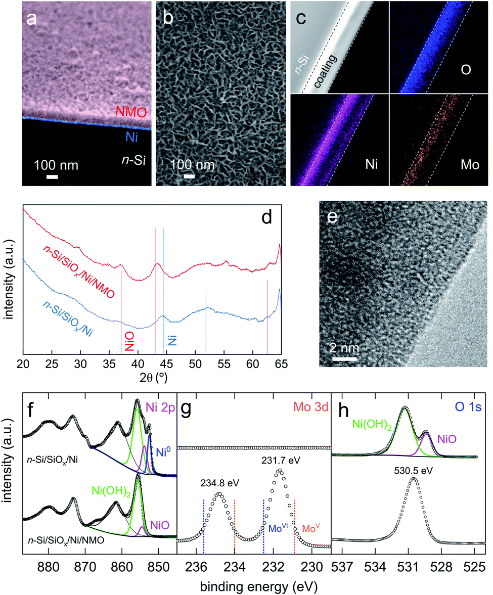 | ||
| Fig. 2 (a) Coloured tilted SEM cross-section picture of a n-Si/SiOx/Ni/NMO surface (original uncoloured picture is shown in Fig. S3c†). (b) SEM top view picture of a n-Si/SiOx/Ni/NMO surface. (c) STEM-ADF (greyscale) and EDS STEM pictures of an n-Si/SiOx/Ni/NMO cross-section showing the O (blue), Ni (purple), and the Mo (orange) content. Dashed lines indicate the boundary of the Ni/NMO layers, which thickness is 105 nm, as determined in the TEM picture of Fig. S11.† (d) XRD patterns of n-Si/SiOx/Ni (blue curve) and n-Si/SiOx/Ni/NMO (red curve) reference Bragg peaks corresponding to Ni (ICSD 64989) and NiO (ICSD 76669) are shown by vertical blue and red lines. (e) High-resolution TEM picture of the NMO coating. (f–h) Ni 2p (f), Mo 3d (g), and O 1s (h) XPS spectra of n-Si/SiOx/Ni (top) and n-Si/SiOx/Ni/NMO (bottom). Disks are experimental data, coloured curves are fits, black curves are the background, and the fit envelope. In (g) the reported binding energies for MoV and MoVI are indicated by dotted lines. | ||
As shown in Fig. 2c–e, surface analyses were performed to determine the nature of the coating. First, the X-ray diffraction (XRD) pattern measured on the modified junction (red curve in Fig. 2d) shows broad peaks with intensity in the same order of magnitude as that of the starting n-Si/SiOx/Ni substrate (blue curve in Fig. 2d). Even though the two higher characteristic peaks present at 2θ = 37.1 and 43.1° can be assigned to the 111 and 200 reflections of NiO, the ill-defined shape and low intensity of these peaks reveal an amorphous nature of the deposited coating (the steep increase around 63–65° is due to the apparatus). This is in good agreement with high-resolution TEM pictures, shown in Fig. 2e and S10† that demonstrate the disorganized structure of the coating at the atomic scale. We attribute the formation of an amorphous phase to the low temperature we employ (mandatory to preserve Si activity) compared to previous works.28–33
X-ray photoelectron spectroscopy (XPS) was also performed before and after deposition, as shown in the top and bottom spectra of Fig. 2f–h, respectively (survey spectra are shown in Fig. S12†). The Ni 2p spectrum (Fig. 2f) obtained for the unmodified n-Si/SiOx/Ni is in good agreement with that of a Ni metal thin film covered by a native NiO/Ni(OH)2 layer.50 After modification, the XPS spectrum considerably changed and the Ni 2p3/2 region could be fitted with three components, namely, two NiII contributions (colored curves) and a broader contribution corresponding to the Ni 2p3/2 satellite peak (black curve). The two NiII components are similar to that generally reported for NiO (854.5 eV) and Ni(OH)2 (855.7 eV).51 The larger relative area for the second contribution suggests that most of the surface Ni atoms are coordinated to OH groups, which is consistent with previous observation on NiO coatings.52Fig. 2g shows that after surface modification, the Mo 3d region presents two peaks corresponding to the 3d5/2 (231.7 eV) and 3d3/2 contributions (234.8 eV) these binding energies are between the common values reported for MoVI (blue dotted line) and MoV (orange dotted line) compounds,53,54 showing that Mo atoms in the layer present a high oxidation state. Ni 2p and Mo 3d spectra fit well with the O 1s spectra recorded after modification, which presents a large peak (fwhm = 2.1 eV) at 530.5 eV. We reasonably assume that this signal is a convolution of several OII− contributions as it spams the binding energies experimentally determined for Ni(OH)2 and NiO (531.7 and 529.4 eV, respectively, Fig. 2h, top), as well as the binding energies reported for OII− in MoO2 (530.0 eV),55 MoO3 (530.7 eV),56 NiMoO4 (530.9 eV),57 and non-stoichiometric MoOx (530.6 eV).58 Besides, chemical mapping using energy-dispersive X-ray spectroscopy performed in scanning transmission electron microscopy (EDS STEM) was performed on the cross-section of a modified surface (a TEM picture of the sample used for this analysis is presented in Fig. S11†). Fig. 2c shows that O, Ni, and Mo atoms are well-dispersed within the entire coating. This figure shows a higher Ni content at the Si interface due to the deposited Ni thin film. In addition, the porosity of the coating results in a higher density at the bottom compared to the top (see also Fig. S11†). Finally, EDS, performed on the modified surface, revealed a Ni/Mo atomic ratio of 9.5. This value is not representative of the ratio in the deposited coating because EDS also probes the underlying (denser) Ni thin film. A more realistic Ni/Mo atomic ratio of 3 was determined from the XPS survey spectra presented in Fig. S12† and is more representative of the composition in the coating. Taken together, these results show that the deposited coating is a porous and amorphous Ni–Mo–O (NMO) material containing high-oxidation-state Mo. Next, we investigate its photoelectrocatalytic activity for UOR (reaction (3)).
Photoelectrochemical UOR
The anodic behaviour of several surfaces was investigated in a 1 M KOH electrolyte containing 0.33 M urea, which is the average concentration in human urine14 and also a benchmark concentration in the UOR literature. Comparative voltammograms are shown in Fig. 3a. While all anodes prepared on photoactive n-Si produced a negligible current in the dark, they exhibited high photocurrent densities (j) under simulated sunlight. Successive cyclic voltammograms (CVs) recorded with a surface prepared without the Ni thin film (n-Si/SiOx/NMO, purple CVs) revealed an onset potential (Eonset, taken arbitrarily for j = 1 mA cm−2) of 1.41 V (all potentials in this article are referred vs. the reversible hydrogen electrode, RHE). In addition, a strong j decrease was noticed while cycling this photoelectrode, after 5 CV cycles, this surface lost 96% of its maximum j value due to photocorrosion. This highlights the importance of the Ni thin film, which is essential to avoid photoanode deactivation.43 Conversely, photoanodes coated with the Ni thin film but not NMO (n-Si/SiOx/Ni, blue CV) had a low Eonset of 0.91 V, attesting a decent activity for UOR. Note that the n-Si/SiOx/Ni surface was also annealed (in the same condition as the other electrodes) because it has been reported that annealing can beneficially influence n-Si/SiOx/Ni junction performance.47 However, without NMO, j decreased strongly after 1.23 V, as a result of the deactivation of the accessible catalytic sites. After the UOR wave, j increases again as OER proceeds (vide infra).59 An interesting aspect of this CV is the sharp peak visible during the backward scan at 1.2 V, attributed to the regeneration of the UOR catalytic sites that were passivated during the forward scan.60 Similar CV shapes corresponding to catalyst deactivation/regeneration have been reported for UOR on Ni60,61 and the oxidation of other molecules on various metals.62,63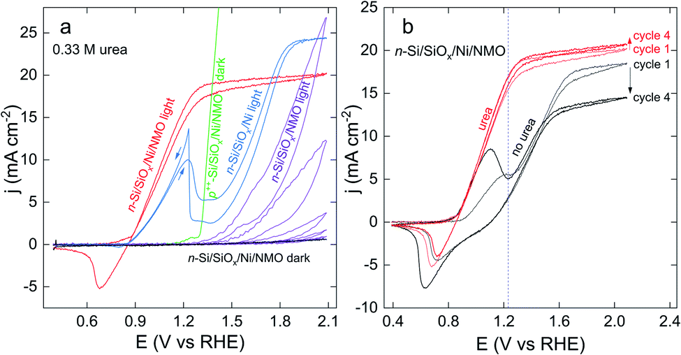 | ||
| Fig. 3 (a) Voltammograms recorded in 1 M KOH + 0.33 M urea in the dark on n-Si/SiOx/Ni/NMO (black curve) and p++-Si/SiOx/Ni/NMO (green curve, forward scan) and under illumination on n-Si/SiOx/NMO (purple curve, 5 successive cycles), n-Si/SiOx/Ni (blue curve, arrows indicate the scan direction), and n-Si/SiOx/Ni/NMO (red curve). (b) 1st (thin line) and 4th (thick line) CVs recorded on illuminated n-Si/SiOx/Ni/NMO in 1 M KOH (black curves) and 1 M KOH + 0.33 M urea (red curves). The standard potential of the O2/H2O couple (1.23 V) is represented by a blue dotted line. The scan rate is 100 mV s−1, the illumination is provided by a solar simulator (100 mW cm−2, AM 1.5G). | ||
On the other hand, photoanodes comprising the Ni thin film and the NMO coating (n-Si/SiOx/Ni/NMO, red CV) exhibited optimal performance, namely a low Eonset of 0.87 V, a high fill factor (as a result of high UOR kinetic)2 and no signs of UOR decay. A non-photoactive degenerate p++-Si surface was also used to manufacture a p++-Si/SiOx/Ni/NMO anode. This electrode was studied in the dark in the same electrolyte, as shown by the green curve in Fig. 3a. The difference between the Eonset measured with this anode and its photoactive counterpart (n-Si/SiOx/Ni/NMO) yields a photovoltage value of 400 mV, consistent with previous studies on photoanodes based on n-Si/SiOx/Ni Schottky junctions.43,64–69
Fig. 3b compares the photoelectrochemical behaviour of an n-Si/SiOx/Ni/NMO photoanode in the presence (red CVs) and the absence of urea (black CVs). In the presence of urea, the CVs obtained at the first (thin line CVs) and the fourth (thick line CVs) cycle are almost identical, revealing good stability of the photoanode for UOR. In the absence of urea, the CVs feature a wave that starts at ≈0.9 V, attributed to the oxidation of NiII(OH)2 in NiIIIOOH. This wave is followed by a j increase caused by OER,70,71 that saturates in the light-limited regime (at the plateau, j = jlim). The reduction wave observed during the backward scan corresponds to the conversion of NiIIIOOH in NiII(OH)2. In passing, we note that, in the absence of urea, jlim depends on the cycle number (this effect will be discussed in detail in the last section). According to this figure, it is clear that a benefit of UOR is that it allows a considerable increase of j at low overpotential. For instance, at the O2/H2O standard potential (1.23 V, depicted by a dotted line in Fig. 3b), j recorded in the presence of urea (17.3 mA cm−2) is more than three times higher than that recorded without urea (5.4 mA cm−2). The effect of urea on the photoanodic response of n-Si/SiOx/Ni/NMO was also assessed by photoelectrochemical impedance spectroscopy (PEIS) measurements at an applied potential of 1 V (Nyquist and Bode plots are presented in Fig. S13†). Fits of the PEIS data resulted in charge transfer resistances at the solid/liquid interface of 3 and 850 Ω in the presence and in the absence of urea, respectively (results are presented in Table S1†), confirming the improved photoelectrochemical performance reached at low overpotential.
Stability during UOR
Next, stability in operation was assessed by potentiostatic measurements. These tests were performed at a low overpotential, a crucial parameter for photoelectrochemical UOR that has been overlooked.36–42 Generally speaking, as previously discussed and shown in Fig. 3b, UOR and OER start at distinct potentials, therefore, to ensure that UOR (and not OER) is actually occurring, it is important to perform stability tests at a low overpotential where OER does not occurs. Indeed, at high overpotential, UOR and OER can occur simultaneously, thus, in the light-limited regime, a loss of the UOR activity can be compensated by the OER, resulting in a stable CA curve even if UOR performance decreases. Indeed, drastic photocurrent decrease at low overpotential but not at high overpotential has been recently reported,41 highlighting that operating photoelectrochemical UOR at high overpotential might lead to biased conclusions. Fig. 4a presents chronoamperograms (CAs) recorded at 1 V, a potential below the OER onset, as seen in the black CV of Fig. 3b. In these conditions, the NMO-free n-Si/SiOx/Ni (blue CA in Fig. 4a) showed a considerable activity decrease, as illustrated by a 70% j loss over 20 min. Conversely, the n-Si/SiOx/Ni/NMO (red CA) exhibited only a 12% j loss in the same timeframe. An experiment was also performed with n-Si/SiOx/Ni/NMO in the same condition except that the electrolyte was free of urea (black CA). Here, j drastically dropped from 5 to 0 mA cm−2 within the first seconds (i.e., after the oxidation of all active Ni(OH)2 sites). This negative control confirms: (i) the necessity of urea to generate high photocurrent densities and, (ii) that OER does not occur at 1 V.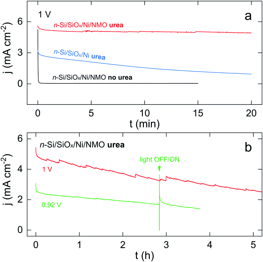 | ||
| Fig. 4 (a) CAs recorded at 1 V under illumination in 1 M KOH without urea on n-Si/SiOx/Ni/NMO (black curve), with 0.33 M urea on n-Si/SiOx/Ni (blue curve) and n-Si/SiOx/Ni/NMO (red curve). (b) CAs recorded under illumination in 1 M KOH with 0.33 M urea on n-Si/SiOx/Ni/NMO at a potential of 1 V (red curve) and 0.92 V (green curve). | ||
Finally, long-term UOR was assessed for this photoanode, as shown in Fig. 4b. The red CA shows that UOR can occur for several hours and that, after 5 hours of photoelectrolysis, j is still half of its initial value. Fig. S14† shows that the photoanode was still active (j > 1 mA cm−2) after 14 h of polarization. The green CA in Fig. 4b shows that n-Si/SiOx/Ni/NMO can also be employed at a lower overpotential with stability. Further, a light interruption at t = 2.8 h (a more resolved CA is shown in Fig. S15†) caused an instantaneous j drop to 0 mA cm−2, which indicates that the photoanode maintained its photoactivity during the test. The strong j spike that is observed when light is switched on is attributed to hole charging.72
To verify UOR occurrence, we used a colorimetric method to measure the urea content in the electrolyte before and after a 3 h-long electrolysis at 1 V (Experimental details are provided in the ESI†). Taking into account a stoichiometric ratio of 6 h+ per molecule of urea electrolyzed (reaction (3)), the measured decrease in urea concentration corresponds to an 85% faradaic efficiency. Conversely, a control experiment showed that illumination of the electrolyte with simulated sunlight during 3 h (without electrode) induced a negligible decrease of urea content (Fig. S16†). After prolonged photoelectrolysis, the n-Si/SiOx/Ni/NMO photoanodes were analyzed by SEM which revealed that the photoanode microscale morphology was not significantly affected by photoelectrolysis (Fig. S17†). Nevertheless, EDS analysis revealed a considerable Mo leaching during operation (Fig. S18†), well in line with recent reports on Mo-containing Ni-based electrocatalysts.73,74 Post-electrolysis XPS measurements (Fig. S12b†) further confirmed Mo leaching as no Mo could be detected after a 15 h-long photoelectrolysis. This is also in agreement with the elemental analysis of the electrolyte that revealed the presence of Mo in solution after photoelectrolysis. These results suggest that Mo is a structuring agent in the NMO coating, which, by dissolving in the electrolyte, increases the surface density of the NiOOH active sites.73,74 Our photoanodes present, by far, the best performance and stability for Si-based photoanodes (Table S2†).41,42 Generally speaking, one can hardly compare the performance of our photoanodes with that reported on other semiconductors36–40 because, as discussed before, in all cases, too high overpotentials are employed to specifically assess UOR (see Table S2†).
Photoelectrochromism and behaviour at high overpotential
Stability in operation was also assessed at high overpotential and showed comparable stability (a CA recorded at an applied potential of 2.1 V is presented in Fig. S19†). As discussed before, at this overpotential, OER is also possible, thus, this CA does not constitute a valid criterion for UOR investigation. Nevertheless, in our specific case, studying the light-limited regime proved particularly interesting to evidence a significant role that urea plays in increasing jlim. Now, we discuss the intriguing behaviour that was reported in Fig. 3b, namely, the fact that the maximum photocurrent obtained for OER decreases with the cycle number while it is not evolving when urea is present in the electrolyte. As seen in Gärtner's relation, jlim (the photocurrent plateau) is proportional to the photon flux reaching the semiconductor.75 Thus, this behaviour suggests that the operation of n-Si/SiOx/Ni/NMO without urea leads to a decreased flux of photons reaching the Si. We show, in the following, that this is caused by the evolution of the optical properties of the NMO coating that induces a deleterious light absorption.NiO coatings are known to be electrochromic, switching from a “bleached” to an “opaque” state when biased at distinct potentials in alkaline electrolytes, as a result of the conversion of Ni(OH)2 into NiOOH.76,77Fig. 5a shows that, without urea, a linear correlation can be made between jlim (recorded at 2.1 V) and the charge integrated under the anodic NiIII/NiII peak during 14 successive CV cycles. This suggests that the jlim loss is caused by the transformation of the Ni(OH)2 into NiOOH. If XPS revealed the presence Ni(OH)2 surface groups after preparation of the surface (Fig. 2f and h), the increase of the charge associated to the NiIII/NiII peak during cycling in the absence of urea (black CVs in Fig. 3b) shows that the amount of Ni(OH)2/NiOOH groups increases upon CV cycling. During OER, Ni(OH)2 is converted into NiOOH which is the active phase of Ni-based electrocatalysts and which is known to strongly absorb light in the visible region.76,77 This is in good agreement with our ex situ transmittance measurements performed on a Ni/NMO coating deposited on indium tin oxide (ITO) substrate (Experimental details are provided in ESI†). Fig. 5b shows that after a 10 min-long OER run, the ITO/Ni/NMO surface exhibits a considerable transmittance decrease, particularly pronounced in the visible range, attesting for the conversion of NMO to an absorbing layer. All these results evidence that the jlim decrease observed by CV during OER on n-Si/SiOx/Ni/NMO (black CVs in Fig. 3b) is caused by the conversion of NMO to an opaque NiOOH-rich catalytic film. These results are in agreement with photoelectrochemical experiments performed with n-Si/SiOx/Ni/NMO made with a thinner NMO coating (42 nm) that resulted in a higher jlim value for OER (Fig. S8a,† thinner NMO film affords higher transmission during OER).
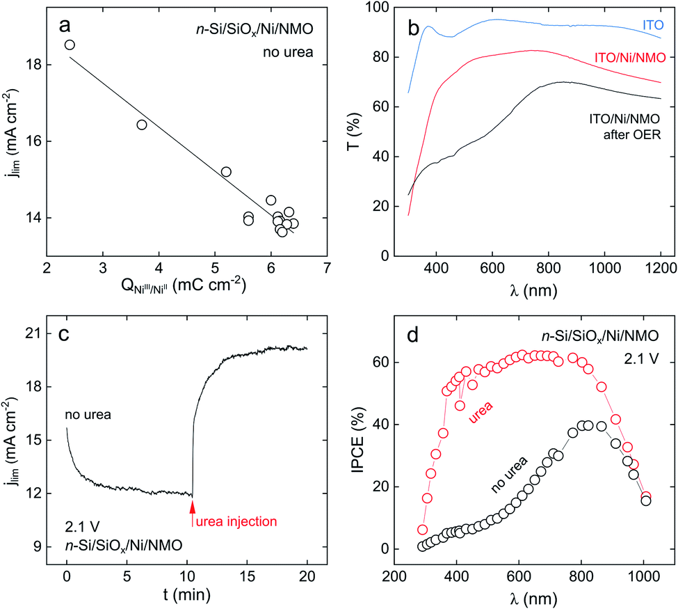 | ||
| Fig. 5 (a) Plot of the photocurrent density at 2.1 V as a function of the charge under the NiIII/NiII peak, extracted from cyclic voltammetry. (b) Transmittance spectra recorded on ITO (blue curve), ITO/Ni/NMO (red curve), and ITO/Ni/NMO after 10 min of OER (black curve). (c) Chronoamperogram recorded while applying 2.1 V under illumination on n-Si/SiOx/Ni/NMO in 1 M KOH without urea, at 10.5 min (red arrow) 0.33 M urea is injected into the cell. (d) IPCE spectra recorded on n-Si/SiOx/Ni/NMO at 2.1 V in 1 M KOH (black curve) and in 1 M KOH + 0.33 M urea (red curve). | ||
The photoelectrochemical behavior of n-Si/SiOx/Ni/NMO is different when urea is present in the electrolyte. As previously observed in the red CVs of Fig. 3b, jlim is not significantly evolving upon photoanode cycling. This observation is corroborated by the potentiostatic experiment shown in Fig. 5c. Here, we applied a potential of 2.1 V to an illuminated n-Si/SiOx/Ni/NMO photoanode in a urea-free electrolyte while recording jlim, and, at 10.5 min, urea was injected in the cell. In the first part of the experiment, jlim decreased due to the formation of NiOOH that decreases light transmission and, in turn, lowers the photocurrent, well in line with the CV observations of Fig. 3b. When urea is injected, jlim instantaneously increases to 20 mA cm−2, the value determined by voltammetry in the red CVs in Fig. 3b.
These results were further confirmed operando by photoelectrochemical spectroscopy. Incident photon-to-current efficiency (IPCE) spectra recorded on n-Si/SiOx/Ni/NMO at 2.1 V are presented in Fig. 5d, in the presence (red spectrum) and the absence of urea (black spectrum). These results show that the photoconversion efficiency is high in the presence of urea, with a maximum IPCE of 60% in the visible range. Conversely, in the absence of urea, the photoconversion efficiency is much lower. This IPCE spectrum presents strong similarities with the transmission spectrum recorded on the ITO/Ni/NMO anode after OER, with a maximum IPCE of 40% at a wavelength (845 nm), that corresponds to the transmittance peak measured ex situ (Fig. 5b). All these results show that urea grants high optical transmission through the NMO coating, promoting higher photocurrent density at high overpotential. Next, we propose an explanation of this effect based on the UOR reaction pathway. Pioneer studies reported that UOR (reaction (3)) at Ni-based electrocatalysts proceeds following an electrochemical–chemical (EC) mechanism as follows:60
| 6Ni(OH)2 (s) + 6OH− (aq) + 6h+ → 6NiOOH (s) + 6H2O (l) | (4) |
| 6NiOOH (s) + (NH2)2CO (aq) + H2O (l) → 6Ni(OH)2 (s) + N2 (g) + CO2 (g) | (5) |
First, Ni(OH)2 is electrochemically converted into NiOOH following reaction (4), then the chemical reaction between NiOOH and urea creates the products and regenerates Ni(OH)2, following reaction (5). In our experiments, in the presence of urea, the conversion of opaque NiOOH into transparent Ni(OH)2 (due to reaction (5)), allows maintaining the high transmittance of NMO and promotes high jlim. Thus, the NMO coating is optically adaptive, enabling optical transmission when UOR occurs. This scenario is very similar to what is known for the electrochemical switching of electrochromic NiO-based films except, that, in our case, a reactant (urea) triggers the optical switch. These results show that in contrast to OER, where the optical performance of the NMO coating is limited by NiOOH, in the presence of urea, the optical properties of the NMO catalytic film are dominated by the Ni(OH)2 phase. This is in good agreement with the size of the cathodic peaks observed in the CVs of Fig. 3b, which reveal a lower amount of electrochemically-addressable NiOOH centers when urea is present.
Conclusions
To conclude, we have reported the preparation and the study of Si-based photoanodes, composed of abundant materials, which can promote solar-assisted UOR for hours. The photoanodes' architecture is based on an n-Si/SiOx/Ni MIS junction onto which an amorphous NMO coating was deposited by a hydrothermal method. In this construct, n-Si is the light absorber, SiOx/Ni grants stability and NMO is the catalytic layer that promotes high UOR activity at low overpotential. Next, focus should be given to the elucidation of the role Mo, which is essential for the hydrothermal growth of the coating onto the MIS structure (Fig. S9†). According to our measurements and recent literature73,74 it also probably acts as a structuring agent in the NMO coating, which, by dissolving in the electrolyte, increases the surface density of the NiOOH active sites. To the best of our knowledge, these photoanodes present the best performance reported so far for photoelectrochemical UOR on silicon (Table S2†). In addition to the outstanding UOR activity, we have reported the optically adaptive nature of the NMO coating, which grants optical transmission of visible light in the presence of urea. In line with the UOR mechanism60 and experimental considerations, we attribute this behaviour to the conversion of NiOOH into Ni(OH)2 which counterbalance the deleterious electrochromic behaviour that occurs in the absence of urea. The investigation of the lifetime of the NiOOH phase during UOR by operando photoelectrochemical methods will bring important elements to obtain additional information on this mechanism. We think that this report presents considerable advances for the valorisation of polluted effluents for solar H2 production and will lead to original strategies for the integration of highly active catalytic layers on semiconductor photoelectrodes.Author contributions
G. L. conceived the idea. G. L., R. A., and D. F. secured funding and co-supervised the research. J. D. developed the preparation method, manufactured the electrodes, and performed the experiments. G. L. and J. D. analyzed the electrochemical results. S. Z., L. S., A. V., V. D., and S. F. performed and analyzed surface characterizations. All authors reviewed and commented on the article.Conflicts of interest
There are no conflicts to declare.Acknowledgements
Loïc Joanny and Francis Gouttefangeas from ScanMAT/CMEBA are acknowledged for SEM analyses. Khalil Youssef is acknowledged for his help with colorimetric titration. Muriel Escadeillas and Bertrand Lefeuvre are acknowledged for their help with elemental analyses.Notes and references
- R. Memming, Semiconductor Electrochemistry, Wiley-VCH, Weinheim, 2015 Search PubMed.
- M. G. Walter, E. L. Warren, J. R. McKone, S. W. Boettcher, Q. Mi, E. A. Santori and N. S. Lewis, Chem. Rev., 2010, 110, 6446–6473 CrossRef CAS PubMed.
- K. Sivula and R. van de Krol, Nat. Rev. Mater., 2016, 1, 15010 CrossRef CAS.
- S. Chen and L.-W. Wang, Chem. Mater., 2012, 24, 3659–3666 CrossRef CAS.
- D. Bae, B. Seger, P. C. K. Vesborg, O. Hansen and I. Chorkendorff, Chem. Soc. Rev., 2017, 46, 1933–1954 RSC.
- S. Y. Reece, J. A. Hamel, K. Sung, T. D. Jarvi, A. J. Esswein, J. J. H. Pijpers and D. G. Nocera, Science, 2011, 334, 645–648 CrossRef CAS PubMed.
- K. Sun, S. Shen, Y. Liang, P. E. Burrows, S. S. Mao and D. Wang, Chem. Rev., 2014, 114, 8662–8719 CrossRef CAS PubMed.
- G. Loget, Curr. Opin. Colloid Interface Sci., 2019, 39, 40–50 CrossRef CAS.
- H. J. Fu, P. Buabthong, Z. P. Ifkovits, W. Yu, B. S. Brunschwig and N. S. Lewis, Energy Environ. Sci., 2022, 15, 334–345 RSC.
- X. G. Zhang, Electrochemistry of silicon and its oxide, Kluwer Academic, 2001 Search PubMed.
- H. J. Fu, I. A. Moreno-Hernandez, P. Buabthong, K. M. Papadantonakis, B. S. Brunschwig and N. S. Lewis, Energy Environ. Sci., 2020, 13, 4132–4141 RSC.
- C. R. Lhermitte and K. Sivula, ACS Catal., 2019, 9, 2007–2017 CrossRef CAS.
- A. N. Rollinson, J. Jones, V. Dupont and M. V Twigg, Energy Environ. Sci., 2011, 4, 1216–1224 RSC.
- B. K. Boggs, R. L. King and G. G. Botte, Chem. Commun., 2009, 4859–4861 RSC.
- K. Ye, G. Wang, D. Cao and G. Wang, Top. Curr. Chem., 2018, 376, 42 CrossRef PubMed.
- B. Zhu, Z. Liang and R. Zou, Small, 2020, 1906133, 1–19 Search PubMed.
- W. Yan, D. Wang and G. G. Botte, Electrochim. Acta, 2012, 61, 25–30 CrossRef CAS.
- S. Periyasamy, P. Subramanian, E. Levi, D. Aurbach, A. Gedanken and A. Schechter, ACS Appl. Mater. Interfaces, 2016, 8, 12176–12185 CrossRef CAS PubMed.
- R. P. Forslund, J. T. Mefford, W. G. Hardin, C. T. Alexander, K. P. Johnston and K. J. Stevenson, ACS Catal., 2016, 6, 5044–5051 CrossRef CAS.
- P. Mirzaei, S. Bastide, A. Dassy, R. Bensimon, J. Bourgon, A. Aghajani, C. Zlotea, D. Muller-Bouvet and C. Cachet-Vivier, Electrochim. Acta, 2019, 297, 715–724 CrossRef CAS.
- C. Wang, H. Lu, Z. Mao, C. Yan, G. Shen and X. Wang, Adv. Funct. Mater., 2020, 30, 2000556 CrossRef CAS.
- F. Cai, L. Liao, Y. Zhao, D. Li, J. Zeng, F. Yu and H. Zhou, J. Mater. Chem. A, 2021, 9, 10199–10207 RSC.
- C. Li, Y. Liu, Z. Zhuo, H. Ju, D. Li, Y. Guo, X. Wu, H. Li and T. Zhai, Adv. Energy Mater., 2018, 8, 1801775 CrossRef.
- R. L. King and G. G. Botte, J. Power Sources, 2011, 196, 9579–9584 CrossRef CAS.
- L. Wang, M. Li, Z. Huang, Y. Li, S. Qi, C. Yi and B. Yang, J. Power Sources, 2014, 264, 282–289 CrossRef CAS.
- X. Song, L. Gao, Y. Li, W. Chen, L. Mao and J.-H. Yang, Electrochim. Acta, 2017, 251, 284–292 CrossRef CAS.
- H. Liu, S. Zhu, Z. Cui, Z. Li, S. Wu and Y. Liang, Nanoscale, 2021, 13, 1759–1769 RSC.
- Y. Tong, P. Chen, M. Zhang, T. Zhou, L. Zhang, W. Chu, C. Wu and Y. Xie, ACS Catal., 2018, 8, 1–7 CrossRef.
- D. Yang, L. Yang, L. Zhong, X. Yu and L. Feng, Electrochim. Acta, 2019, 295, 524–531 CrossRef CAS.
- Z.-Y. Yu, C.-C. Lang, M.-R. Gao, Y. Chen, Q.-Q. Fu, Y. Duan and S.-H. Yu, Energy Environ. Sci., 2018, 11, 1890–1897 RSC.
- L. Sha, T. Liu, K. Ye, K. Zhu, J. Yan, J. Yin, G. Wang and D. Cao, J. Mater. Chem. A, 2020, 8, 18055–18063 RSC.
- Q. Xu, T. Yu, J. Chen, G. Qian, H. Song, L. Luo, Y. Chen, T. Liu, Y. Wang and S. Yin, ACS Appl. Mater. Interfaces, 2021, 13, 16355–16363 CrossRef CAS.
- J.-Y. Zhang, T. He, M. Wang, R. Qi, Y. Yan, Z. Dong, H. Liu, H. Wang and B. Y. Xia, Nano Energy, 2019, 60, 894–902 CrossRef CAS.
- X. An, D. Stelter, T. Keyes and B. M. Reinhard, Chem, 2019, 5, 2228–2242 CAS.
- G. Shao, Y. Zang and B. J. Hinds, ACS Appl. Nano Mater., 2019, 2, 6116–6123 CrossRef CAS.
- J. Liu, J. Li, M. Shao and M. Wei, J. Mater. Chem. A, 2019, 7, 6327–6336 RSC.
- G. Wang, Y. Ling, X. Lu, H. Wang, F. Qian, Y. Tong and Y. Li, Energy Environ. Sci., 2012, 5, 8215–8219 RSC.
- D. Xu, Z. Fu, D. Wang, Y. Lin, Y. Sun, D. Meng and T. feng Xie, Phys. Chem. Chem. Phys., 2015, 17, 23924–23930 RSC.
- J. Gan, B. B. Rajeeva, Z. Wu, D. Penley and Y. Zheng, J. Appl. Electrochem., 2020, 50, 63–69 CrossRef CAS.
- R. Zhao, G. Schumacher, S. Leahy and E. J. Radich, J. Phys. Chem. C, 2018, 122, 13995–14003 CrossRef CAS.
- G. Loget, C. Mériadec, V. Dorcet, B. Fabre, A. Vacher, S. Fryars and S. Ababou-Girard, Nat. Commun., 2019, 10, 3522 CrossRef CAS PubMed.
- P. Aroonratsameruang, P. Pattanasattayavong, V. Dorcet, C. Mériadec, S. Ababou-Girard, S. Fryars and G. Loget, J. Phys. Chem. C, 2020, 124, 25907–25916 CrossRef CAS.
- M. J. Kenney, M. Gong, Y. Li, J. Z. Wu, J. Feng, M. Lanza and H. Dai, Science, 2013, 342, 836–840 CrossRef CAS PubMed.
- T. Han, Y. Shi, X. Song, A. Mio, L. Valenti, F. Hui, S. Privitera, S. Lombardo and M. Lanza, J. Mater. Chem. A, 2016, 4, 8053–8060 RSC.
- F. A. L. Laskowski, M. R. Nellist, R. Venkatkarthick and S. W. Boettcher, Energy Environ. Sci., 2017, 10, 570–579 RSC.
- K. Sun, N. L. Ritzert, J. John, H. Tan, W. Hale, J. Jiang, I. A. Moreno-Hernandez, K. M. Papadantonakis, T. P. Moffat, B. S. Brunschwig and N. Lewis, Sustainable Energy Fuels, 2018, 2, 983–998 RSC.
- S. Li, G. She, C. Chen, S. Zhang, L. Mu, X. Guo and W. Shi, ACS Appl. Mater. Interfaces, 2018, 10, 8594–8598 CrossRef CAS PubMed.
- J. R. Hemmerling, A. Mathur and S. Linic, Acc. Chem. Res., 2021, 54, 1992–2002 CrossRef CAS PubMed.
- K. Oh, C. Mériadec, B. Lassalle-Kaiser, V. Dorcet, B. Fabre, S. Ababou-Girard, L. Joanny, F. Gouttefangeas and G. Loget, Energy Environ. Sci., 2018, 11, 2590–2599 RSC.
- H. J. Mathieu, M. Datta and D. Landolt, J. Vac. Sci. Technol., A, 1985, 3, 331–335 CrossRef CAS.
- C. D. Wagner, J. F. Moulder, L. E. R. Davis and W. M. Riggs, Hand Book of X-Ray Photoelectron Spectroscopy, 2008, vol. 3 Search PubMed.
- M. K. S. Barr, L. Assaud, Y. Wu, C. Laffon, P. Parent, J. Bachmann and L. Santinacci, Electrochim. Acta, 2015, 179, 504–511 CrossRef CAS.
- J.-G. Choi and L. T. Thompson, Appl. Surf. Sci., 1996, 93, 143–149 CrossRef CAS.
- T.-G. Truong, C. Meriadec, B. Fabre, J.-F. Bergamini, O. de Sagazan, S. Ababou-Girard and G. Loget, Nanoscale, 2017, 9, 1799–1804 RSC.
- D. S. Zingg, L. E. Makovsky, R. E. Tischer, F. R. Brown and D. M. Hercules, J. Phys. Chem., 1980, 84, 2898–2906 CrossRef CAS.
- B. Brox and I. Olefjord, Surf. Interface Anal., 1988, 13, 3–6 CrossRef CAS.
- S. Kasztelan, J. Grimblot, J. P. Bonnelle, E. Payen, H. Toulhoat and Y. Jacquin, Appl. Catal., 1983, 7, 91–112 CrossRef CAS.
- M. Anwar, C. A. Hogarth and R. Bulpett, J. Mater. Sci., 1989, 24, 3087–3090 CrossRef CAS.
- V. Vedharathinam and G. G. Botte, Electrochim. Acta, 2012, 81, 292–300 CrossRef CAS.
- V. Vedharathinam and G. G. Botte, Electrochim. Acta, 2013, 108, 660–665 CrossRef CAS.
- N. A. M. Barakat, M. Motlak, Z. K. Ghouri, A. S. Yasin, M. H. El-Newehy and S. S. Al-Deyab, J. Mol. Catal. A: Chem., 2016, 421, 83–91 CrossRef CAS.
- Z. X. Liang, T. S. Zhao, J. B. Xu and L. D. Zhu, Electrochim. Acta, 2009, 54, 2203–2208 CrossRef CAS.
- G. A. El-Nagar, A. M. Mohammad, M. S. El-Deab and B. E. El-Anadouli, RSC Adv., 2016, 6, 29099–29105 RSC.
- G. Loget, B. Fabre, S. Fryars, C. Mériadec and S. Ababou-Girard, ACS Energy Lett., 2017, 2, 569–573 CrossRef CAS.
- K. Oh, O. de Sagazan, C. Léon, S. Le Gall and G. Loget, Nanoscale, 2021, 13, 1997–2004 RSC.
- G. Xu, Z. Xu, Z. Shi, L. Pei, S. Yan, Z. Gu and Z. Zou, ChemSusChem, 2017, 10, 2897–2903 CrossRef CAS PubMed.
- J. Zhao, T. M. Gill and X. Zheng, Nano Res., 2018, 11, 3499–3508 CrossRef CAS.
- S. A. Lee, T. H. Lee, C. Kim, M. G. Lee, M.-J. Choi, H. Park, S. Choi, J. Oh and H. W. Jang, ACS Catal., 2018, 8, 7261–7269 CrossRef CAS.
- Y. Zhao, J. Yu, G. Xu, N. Sojic and G. Loget, J. Am. Chem. Soc., 2019, 141, 13013–13016 CrossRef CAS PubMed.
- S. L. Medway, C. A. Lucas, A. Kowal, R. J. Nichols and D. Johnson, J. Electroanal. Chem., 2006, 587, 172–181 CrossRef CAS.
- D. S. Hall, C. Bock and B. R. MacDougall, J. Electrochem. Soc., 2013, 160, F235–F243 CrossRef CAS.
- L. Peter, in Photoelectrochemical water splitting: materials, processes and architectures, The Royal Society of Chemistry, 2013, pp. 19–51 Search PubMed.
- X. Liu, J. Meng, K. Ni, R. Guo, F. Xia, J. Xie, X. Li, B. Wen, P. Wu, M. Li, J. Wu, X. Wu, L. Mai and D. Zhao, Cell Rep. Phys. Sci., 2020, 1, 100241 CrossRef.
- R. N. Dürr, P. Maltoni, H. Tian, B. Jousselme, L. Hammarström and T. Edvinsson, ACS Nano, 2021, 15, 13504–13515 CrossRef PubMed.
- W. W. Gärtner, Phys. Rev., 1959, 116, 84–87 CrossRef.
- Y. Ren, W. K. Chim, L. Guo, H. Tanoto, J. Pan and S. Y. Chiam, Sol. Energy Mater. Sol. Cells, 2013, 116, 83–88 CrossRef CAS.
- H. Moulki, D. H. Park, B.-K. Min, H. Kwon, S.-J. Hwang, J.-H. Choy, T. Toupance, G. Campet and A. Rougier, Electrochim. Acta, 2012, 74, 46–52 CrossRef CAS.
Footnote |
| † Electronic supplementary information (ESI) available. See https://doi.org/10.1039/d2ta01212j |
| This journal is © The Royal Society of Chemistry 2022 |