 Open Access Article
Synthesis of CuOx nanostructures in novel electrolytes under hydrodynamic conditions for photoelectrochemical applications†
G.
Sánchez-García
 a,
A.
Pérez-Calvo
a,
R. M.
Fernández-Domene
a,
E.
Blasco-Tamarit
b,
R.
Sánchez-Tovar
*a and
B.
Solsona
a,
A.
Pérez-Calvo
a,
R. M.
Fernández-Domene
a,
E.
Blasco-Tamarit
b,
R.
Sánchez-Tovar
*a and
B.
Solsona
 *a
*a
aDepartment of Chemical Engineering, Universitat de València, Av. Universitats s/n, 46100 Burjassot, Spain. E-mail: rita.sanchez@uv.es; benjamin.solsona@uv
bInstituto Universitario de Seguridad Industrial, Radiofísica y Medioambiental (ISIRYM), Universitat Politècnica de València, Camino de Vera s/n, 46022, Valencia, Spain
First published on 15th September 2023
Abstract
In this work, CuOx (x = 1 and 2) nanostructures have been synthesized by electrochemical anodization in ethylene glycol based electrolytes using oxalic acid or NaF (with or without NaOH) as complexing agents. The influence of hydrodynamic conditions and time during anodization of copper have also been evaluated. A comprehensive morphological, structural, electrochemical and photoelectrochemical characterization of the nanostructures has been performed. The results revealed the convenient use of oxalic acid and 250 rpm for 5 minutes during electrochemical anodization to obtain homogeneous CuOx nanostructures formed by spheres with Cu2O as a predominant phase. Using this nanostructure as a photocathode for N2O photoelectron-reduction, almost 100% of N2O removal was achieved after 1 h, showing the improvement of the photoelectrochemical approach vs. the photo or the electro performance.
Introduction
In recent years, semiconductor metal oxides have become very promising candidates for numerous applications. In particular, extensive research is being done on copper oxides (Cu2O and CuO) and their many morphologies. Furthermore, these materials have a wide range of possible uses due to their suitable characteristics, such as low toxicity, inexpensiveness, narrow bandgaps, very negative conduction band positions, and excellent thermal and electrical conductivities.1,2Nowadays, copper oxide (I and II) films with different nanostructural morphologies (nanospheres, nanoboxes, nanocubes, etc.2,3) have been synthesized using a wide variety of techniques. Some of these methods include pulverization pyrolysis, spin coating, direct heating of the copper films, and hydrothermal synthesis.3–6 However, a lack of control in these methods can lead to variations in the crystal quality, which can alter the surface morphology of the nanostructures and, therefore, affect their physical, structural, and chemical properties, as well as their optoelectronic properties.2,7
Additionally, the preparation of the electrodes has poor stability, and in most of the procedures, toxic chemicals are used. Among the studied alternatives, the electrochemical route appears to be one of the most appropriate due to its low cost, controllability, and minimal environmental impact.7 Electrochemical anodization offers a large number of advantages, including the ability to adequately control the properties of copper oxide films, its speed compared to other techniques, its stability, and its appropriate scalability. Nevertheless, the use of this technology for the synthesis of copper oxide films has only been developed in a small number of studies. The work of D. W. Shoesmith et al. (1976)8 constitutes the first report on nanocrystal growth on copper by potentiostatic oxidation using LiOH solution. Later, in 1990 Ji et al.9 studied the influence of the electrolyte temperature on the process as well as the effect of different additives. In recent years, copper anodization has been carried out using mostly aqueous electrolytes (or even ethylene glycol electrolytes) containing KOH, NaOH, KCl, and NH4Cl.7,10–12 However, none of the investigations have involved the synthesis of novel ethylene glycol based electrolytes with the addition of oxalic acid or NaF as the complexing agent.
Usually, metallic oxides used in optoelectronic applications, such as TiO2, WO3, or ZnO, are n-type semiconductors, which means that they are electron-carrying oxides. On the other hand, attention has been drawn to the use of copper oxides as photocathodes due to their p-type semiconductor properties, like their high absorption coefficient in the UV-vis region. Additionally, both have narrow bandgaps: 1.3–1.7 eV (CuO) and 2.0–2.5 eV (Cu2O).13
According to band gap values, copper(II) oxide is better suited thermodynamically to achieve higher efficiencies than Cu2O. However, given that the mobility of charges in Cu2O is much higher than in CuO (100 cm2 V−1 s−1 and 0.1 cm2 V−1 s−1, respectively) and that Cu2O has a greater p-type character due to the presence of a higher number of copper vacancies,13 it can be inferred that the synthesis of nanostructures where Cu2O predominates could be more interesting. Besides, some studies14,15 confirm the enhancement of the photoelectrochemical response when CuOx nanostructures with both Cu+ and Cu2+ are present.
Due to all the reasons mentioned above, copper oxides are being investigated as photoelectrodes in a wide range of applications to address current environmental challenges.4,16–18 Their potential applications include their use as a photocathode in the breakdown of water to produce hydrogen (water splitting) or their use in the decomposition of other inorganic compounds, such as the main greenhouse gas produced due to human activities, CO2. N2O is the third most abundant greenhouse gas in the atmosphere with a global warming potential (GWP) 273 times that of CO2 for a 100-year timescale.19 Human activities such as agriculture, fuel combustion, industrial processes and wastewater management are increasing the amount of N2O in the atmosphere.20 Besides, nitrous oxide has been identified as the main anthropogenic ozone-depleting substance emitted in this century.21 For this reason, the photoelectrocatalytic decomposition of N2O can be an attractive option to reduce its concentration in the principal emission sources and mitigate climate change.
The goal of this paper is to synthesize copper oxide nanostructures by electrochemical anodization by varying the anodization parameters (electrolyte, time and the use of hydrodynamic conditions) and characterize their morphology, structure, electrochemical and photoelectrochemical properties to investigate their potential use in photoelectrochemical applications.
According to the results, the photoelectrochemical decomposition of N2O was carried out using the synthesized copper oxide nanostructure as a photocathode, achieving almost 100% of N2O removal after 1 h. To our knowledge, this is the first paper that follows the photoelectrochemical approach under mild conditions (room temperature and atmospheric pressure) to photoelectro-reduce N2O.
Experimental
Synthesis of CuOx nanostructures
For the fabrication of the CuOx nanostructures, copper foils (99.9%, 0.125 mm thick) were washed using an ultrasonic bath for 15 seconds in 0.1 M HCl and 30 seconds in acetone, ethanol, and deionized water, respectively and then dried with a flow of N2.The anodization of copper was performed using a two-electrode electrochemical cell with the copper sheet as the working electrode and platinum foil as the counter electrode. The experimental variables were the electrolyte, the anodization time and the use of hydrodynamic conditions.
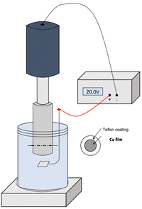
All the tests were carried out by connecting the working electrode to a rotating disk electrode, RDE, (Fig. 1), with an exposed area of the copper foil to the electrolyte of 1.32 cm2. An optical picture of the real anodization device is shown in Fig. S1.†
Copper was first anodized in 70% (v/v) ethylene glycol (EG) and 30% (v/v) deionized water with different complexing agents, both in 0.05 M: oxalic acid and sodium fluoride. The influence of the presence of 0.1 M NaOH in these solutions was also studied.
The samples were anodized in each solution for different times (5, 10 and 15 minutes) at 50 °C and a voltage of 20 V.
To optimize the synthesis, different ethylene glycol concentrations (50 and 90%), as well as different organic bases namely formamide (FA) and ethanol (EtOH), at 50, 70 and 90% were used for anodization.
To evaluate the influence of hydrodynamic conditions during anodization, films were anodized by varying the RDE revolutions at 0, 250 and 500 rpm.
After anodization, foils were carefully cleaned with ethanol and deionized water before being dried with a N2 stream. Afterwards, samples were annealed in air at 250 °C for 1 h.
Characterization of the copper oxide nanostructures
CuOx nanostructures were characterized using different techniques to evaluate their morphology, crystallinity and electrochemical and photoelectrochemical properties. The morphological study was carried out by field emission scanning electron microscopy (FE-SEM, Hitachi S4800 microscope) at an operation voltage of 5 kV, by coating the nanostructures with Au/Pd by sputtering. Additionally, high-resolution transmission electron microscopy (HRTEM) using a FEI Tecnai G2 F20 TWIN with an operation voltage of 200 kV was also used to analyze the copper oxide samples. TEM calibration was performed in two modes: (i) in low and medium magnification modes using catalase crystals (product no. 612) as a reference sample and (ii) in the high magnification mode, in which the resolution and the calibration were verified using nanoparticles of crystalline gold.In order to evaluate the chemical structure of the samples confocal laser-Raman spectroscopy (WITec) with a blue laser (488 nm) was used. Crystallinity and phase identification were carried out using an X-ray diffractometer (XRD) with a Philips X'Pert diffractometer equipped with a graphite monochromator operating at 40 kV and 30 mA, and employing nickel-filtered CuKα radiation (λ = 0.1542 nm). Additionally, a UV-visible spectrophotometer (Shimadzu) in the wavelength range of 200–800 nm was used to determine the photochemical response of the CuOx nanostructures.
Electrochemical and photoelectrochemical characterization studies were carried out in a three electrode cell with the anodized Cu film as the anode, platinum as the counter electrode and Ag/AgCl (3 M KCl) as the reference electrode, using an electrolyte solution of 0.1 M Na2SO4. Electrochemical impedance spectroscopy (EIS) tests were performed at −0.2 VAg/AgCl using an amplitude of 0.01 V and scanning frequencies from 100 kHz to 0.01 Hz. Besides, in order to know the semiconductor character of the nanostructures Mott–Schottky (MS) plots were carried out at a frequency of 5000 Hz, scanning the potential from 0.1 to −0.5 VAg/AgCl. Photoelectrochemical characterization was conducted by scanning the potential from 0 to −0.8 VAg/AgCl alternating dark and illumination conditions (16 s dark, 4 s illumination) with UV light (λ = 365 nm) provided by a LedControl UV LED (Opystec Dr Gröbel Germany) at a power of 100 mW cm−2.
Photoelectrodegradation approach with copper oxide nanostructures
In order to evaluate the photoelectrochemical approach of the CuOx nanostructure samples were used as photocathodes for N2O removal. Fig. 2 shows the H type cell used for N2O reduction.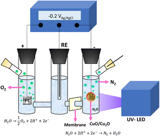 | ||
| Fig. 2 Schematic diagram of the photoelectrocatalytic cell for N2O degradation and oxygen evolution. | ||
The developed copper oxide nanostructure was employed as a cathode, while a saturated Ag/AgCl (3 M KCl) electrode and a platinum sheet were used as reference and counter electrodes, respectively. Both were separated from the anode by a cationic membrane (Nafion N-117 membrane of 0.180 mm thick). The solution (0.1 M Na2SO4) was saturated with N2O before beginning the test and was stirred during the experiment (2 hours).
Three different approaches were carried out to reduce N2O, namely electrocatalytic, photocatalytic and photoelectrocatalytic. For the electrocatalytic decomposition −0.2 VAg/AgCl were applied to the system and no light was irradiated to the nanostructure, while for the photocatalytic reduction only UV-light (λ = 365 nm at a power of 100 W cm−2) was irradiated.
For the photoelectrocatalytic approach a constant potential of −0.2 VAg/AgCl was applied and the cathode was irradiated by UV light. To know the efficiency of decomposition, the evolution of N2O composition inside the cell was measured by taking samples of the stagnant liquid and introducing them into sealed vials.
After that and once equilibrium was reached, the composition of the gas inside the vial was analyzed using an online gas chromatograph (Agilent 7890A).
Results and discussion
Influence of the electrolyte
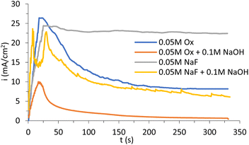
Fig. 3 shows the current density–time curves registered for 5 minutes during the anodization of copper using the different electrolytes with 70% (v/v) EG: oxalic acid (Ox) and NaF 0.05 M with and without NaOH, under stagnant conditions (i.e. at 0 rpm).In all cases, similar profiles were shown for the samples anodized in different electrolytes at longer times (see Fig. S2,† where representative images of the CuOx samples anodized at different times are shown).
According to Fig. 3, first, the current density increases due to the slow application of the working potential (20 V).
Once the full potential is applied, electrolytes containing oxalic acid present the typical anodization curve for nanostructure formation, where the current density steadily drops until reaching a more or less constant value. This situation can be attributed to the formation of a thin layer of precipitate, which is later re-dissolved forming the nanostructure. Different curve shapes can be appreciated in Fig. 3. For example, the NaF curve suggests that the precipitate layer does not quite form during the anodization process, leading to a different morphology. Moreover, adding NaOH to this electrolyte facilitates the formation of the layer, since a decrease in current density is observed. In that case (NaF + NaOH), a double current density peak is observed at the beginning of the process, which is probably related to a dissolution–precipitation mechanism preceded by the formation of a soluble and unstable initial layer. However, with oxalic acid, regardless of the use of NaOH, the precipitate layer is formed, as can be observed in both curves in Fig. 3.
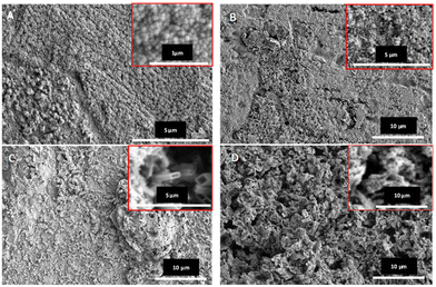
After anodization, samples were covered in a thin blue precipitate, but most of this precipitate was washed away when samples were rinsed with D.I. water. The surface morphology of the copper oxide nanostructures was analyzed through field emission scanning electron microscopy (FE-SEM) and the representative images are shown in Fig. 4. Fig. 4 confirms the growth of copper oxide nanostructures. However, different morphologies can be observed when the anodization electrolyte is changed. Copper oxide films anodized with a 0.05 M oxalic acid electrolyte show a more uniform morphology, where nanostructures are present as spheres (Fig. 4A), with an average diameter of 0.91 nm.
Comparing Fig. 4A and C, it is clear that the use of NaF as a complexing agent involves the formation of a more heterogeneous surface. The magnification of Fig. 4C reveals the existence of brick-like nanostructures in some locations of the films, but also unshaped regions. The effect of NaOH can be observed when comparing Fig. 4A with B and C with D, where thicker layers are formed but in a much more heterogeneous way as the nanoparticles lose their shape.
The XRD patterns of the copper oxide films prepared with different anodization electrolytes are shown in Fig. 5.
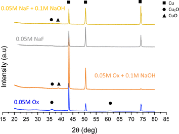 | ||
| Fig. 5 XRD patterns of copper oxide nanostructures after anodization at 20 V and 50 °C in different electrolytes with 70% (v/v) EG and at 0 rpm. | ||
Fig. 5 shows that the major diffraction peaks observed at 2θ = 43.4°, 50.4° and 74.1° are assigned to the (111), (200) and (220) planes of the Cu substrate respectively.12,22 Other smaller peaks can be observed at 2θ = 36.5°, 38° and 61.5°.
The first and last peaks correspond to the diffraction from the (111) and (220) planes of Cu2O, respectively,1,12,23 while the second one belongs to the (200) plane of CuO.22,24 Fig. S3† shows the magnification of this figure, where some peaks can be appreciated more clearly.
Depending on the electrolyte used, one salt or another is formed. When the electrolyte contains NaOH or the complexing agent is NaF (basic solution), the following reaction (eqn (1)) takes place.
| Cu + 2OH− → Cu(OH)2 + 2e− | (1) |
However, in a 0.05 M oxalic acid electrolyte where OH− is not present, the salt formed is copper oxalate (eqn (2)).
| Cu + C2O42− → CuC2O4 + 2e− | (2) |
The final oxide phases are reached during annealing, where copper hydroxide and copper oxalate decomposed into a mixture of CuO and Cu2O.25 Furthermore, when copper is anodized in a basic solution, it starts to release Cu2+ ions.22,24 Therefore, it is reasonable that a higher amount of CuO is present in nanostructures where NaOH was added to the anodization electrolyte, given that sodium hydroxide makes the pH of the solution more basic.
Fig. 6 shows the Raman spectra of the copper oxide nanostructures. These results also reveal the presence of both copper oxide phases in all samples. As has been outlined above, a mixture of both phases is formed during annealing due to the decomposition of copper hydroxide and/or copper oxalate. The peaks at 145, 218 and 636 cm−1 correspond to Cu2O,1,23 while peaks at 293, 342 and 620 cm−1 belong to CuO.1,23
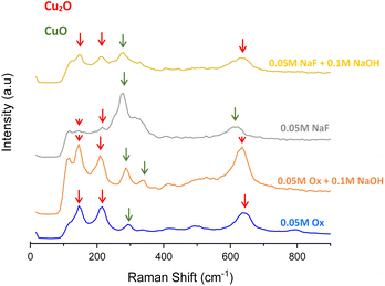 | ||
| Fig. 6 Raman spectra of Cu2O/CuO nanostructures prepared with different anodization electrolytes with 70% (v/v) EG and at 0 rpm. | ||
Although both phases are present in every nanostructure, several differences can be noticed. For example, the presence of Cu2O is higher in samples anodized with oxalic-containing electrolytes, since peaks at 145, 218 and 636 cm−1 are more defined than in the samples anodized with NaF. In the same way, CuO prevails over Cu2O when the complexing agent used during anodization is NaF, as the intensity of Cu2O peaks decreases and peaks at 293, 342 and 620 cm−1 belonging to CuO grow.
When oxalic acid is used as a complexing agent the reaction in eqn (2) takes place and copper oxalate is formed. Copper oxalates have some of their Raman peaks at 209, 290, 611 and 830 cm−1.26,27
Studying the Raman spectra of the samples anodized with oxalic acid before the heat treatment (Fig. S4†), it can be confirmed how copper oxalate Raman peaks are present. Once the samples are annealed, it is clear that copper oxalate also decomposes into a mixture of copper oxides, where Cu2O is predominant, as shown in Fig. S4†. Therefore, it makes sense that samples anodized with oxalic acid have more cuprous oxide than samples anodized with NaF.
On the other hand, it is observed that both oxides appear in similar ratios when NaOH is added to the electrolyte. This is in accordance with the XRD results, since the NaF electrolyte is basic and adding NaOH to the oxalic acid solution also increases its pH, allowing CuO to form in both cases.22,24
These Cu–oxide samples have been also characterized by DR-UV-Vis in order to understand the interactions of the samples with visible and ultraviolet light. In this manner, we can record spectra that can corroborate the nature of the Cu compounds present in the samples as well as obtain information about their physical and electronic structures.
Fig. 7 shows the absorbance spectra of several copper oxides prepared under static conditions employing different compounds for the synthesis of nanostructures.
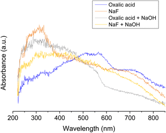 | ||
| Fig. 7 DR-UV-Vis spectra of CuOx nanostructures prepared with different anodization electrolytes with 70% (v/v) EG and at 0 rpm. | ||
The nature of the complexing agents employed was shown as a determinant in the shape of the spectra. Thus, the sample prepared in the presence of oxalic acid shows the main absorbance band between 380 and 550 nm whereas that prepared in NaF presents the main band between 240 and 380 nm, centered at ca. 300 nm.
The band at intermediate wavelengths (380–550 nm) has been related to the presence of Cu+ as in Cu2O28,29 whereas that at ca. 300 nm is typical of Cu2+ species as in CuO.29 It has been also reported29,30 that CuO enhances the absorption at high wavelengths (600–800 nm) although, in our samples, a clear trend has not been observed. Therefore, according to our spectra the use of oxalic acid favors the formation of copper oxide in a relatively reduced oxidation state whereas the use of NaF leads to the main formation of copper oxide, with Cu in its highest possible valence. In any case, a precise phase assignment from UV-Vis is not totally conclusive and it is very likely the co-existence of both oxides. Unexpectedly, the use of NaOH apart from oxalic acid or NaF gives rise to opposite tendencies. Then, the addition of NaOH to either NaF or oxalic acid leads to a wide band from ca. 200 nm to 600–800 nm, suggesting the formation of both CuO and Cu2O. This indicates that the mean Cu oxidation state of the nanostructures in the case of samples prepared with oxalic acid increases upon the addition of NaOH whereas it decreases in the case of NaF.
This analysis is consistent with XRD and Raman spectra results, confirming the existence of both oxide phases in all copper nanostructures, but prevailing one oxide over the other depending on the complexing agent used during anodization.
Fig. 8 shows the photocurrent densities vs. potential curves for the nanostructures anodized in the different electrolytes under stagnant conditions. According to Fig. 8, all anodized samples act as p-type semiconductors since photocurrent densities are negative under illumination (cathode photocurrent).
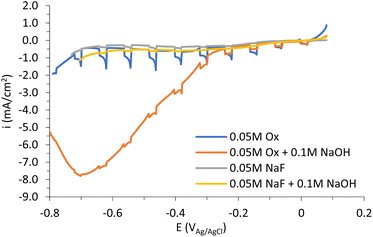 | ||
| Fig. 8 Photocurrent transient vs. potential for the copper oxide nanostructures formed using different electrolytes with 70% (v/v) EG at 0 rpm under UV-light (λ = 365 nm). | ||
Furthermore, it is clear that copper oxide films synthesized using the 0.05 M oxalic acid electrolyte possess the highest photocurrent density (in absolute value) over the rest. This result could be associated with several facts.
First, Fig. 4 shows that the nanostructure with the best photoelectrochemical behavior (0.05 M Ox) presents the most homogeneous morphology, as well as the formation of spheres, leading to better charge carrier mobility. The higher photocurrent density can be also the result of a CuOx mixed oxide (CuO and CuO2) with a major presence of highly (111) oriented Cu2O (Fig. 5), where the hole collection efficiency is better.31,32 Moreover, the presence of copper metal is known to reduce the photoactivity of the nanostructures.1,33 Therefore, it makes sense that the 0.05 M Ox sample, which is the nanostructure with the lowest Cu metal content (as seen in Fig. 5), has the best photoelectrochemical response.
In summary, it is clear from Fig. 6 that oxalic acid containing electrolytes produce nanostructures with more Cu2O than NaF containing electrolytes, where CuO prevails. Although cupric oxide has a narrower band gap (1.3–1.8 eV), related to better light absorption, cuprous oxide has more p-type character due to the higher number of copper vacancies and presents much better mobility of these holes.13 Hence, it can be inferred that having a mixture of both oxide phases, but with a major presence of cuprous oxide, has a positive effect on the photoelectrochemical performance of the nanostructures.
Additionally, it is important to point out that when anodization was carried out at longer times, photocurrent values did not increase or even decrease at 15 minutes (see Fig. S5†). This could be related to the lower number of spheres with larger diameters exposed to the electrolyte when anodization was performed at 10 or 15 minutes, since sphere density decreased from 1556 spheres per m2 at 5 min to 201 and 182 spheres per m2 at 10 and 15 min, respectively (see Fig. S6†).
For the nanostructure which presented the best photoelectrochemical response, that is, the one anodized with 0.05 M oxalic acid, samples were anodized with different ethylene glycol amounts (50 and 90% (v/v)) and in different electrolytes (ethanol and formamide at 50, 70 and 90% (v/v)). Amounts below 50% (v/v) were not tested due to the vigorous bubble formation during anodization and, therefore, results were not reproducible.
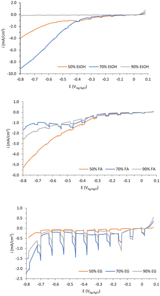
Fig. 9 shows the photocurrent densities vs. potential curves for the nanostructures anodized in the mentioned electrolytes.
According to Fig. 9, ethylene glycol-based electrolytes enhance the photoelectrochemical response of the catalysts, especially when working with 70% (v/v).
Fig. S7† shows some FE-SEM representative images of the samples anodized with EG (50% and 90% (v/v)), FA (70% (v/v)), and EtOH (70% (v/v)).
Regarding the EG samples, it is clear that the sample anodized in EG electrolytes containing 50% (v/v) (Fig. S7a†) presents a heterogeneous surface, where nanoparticles are not completely formed. On the other hand, with 90% (v/v) EG (Fig. S7b†) the formed nanoparticles were too packed together, which can prevent the active surface from absorbing light, hence producing lower photocurrents.
Samples anodized in both ethanol (Fig. S7c†) and formamide (Fig. S7d†) electrolytes have extremely amorphous nanostructures with no clear geometry. The amorphous morphology leads to worse charge carrier mobility, since the direct pathways for electron transfer provided by the ordered spheres disappear due to the presence of irregular blocks. This results in more charge recombination and lower efficiency of electron transfer,34 hence leading to bad photoelectrochemical behavior of both solvents compared to ethylene glycol.
Influence of hydrodynamic conditions
Once the best nanostructure was determined (that prepared with 0.05 M oxalic acid in a 70% (v/v) ethylene glycol-based electrolyte), the influence of hydrodynamic conditions in the anodization process was studied, rotating the copper electrode at 250 and 500 rpm.The anodization curves of the samples synthesized under different hydrodynamic conditions are shown in Fig. 10.
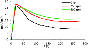 | ||
| Fig. 10 Current density curves registered during electrochemical anodization in 70% (v/v) EG with 0.05 M oxalic acid at 20 V and 50 °C under different hydrodynamic conditions (0 to 500 rpm). | ||
Current density curves displayed in Fig. 10 follow the same tendency as the curves shown in Fig. 3. However, some differences can be highlighted.
As the rotation speed gets more vigorous, the current density decrease is more gradual, which means that nanostructure formation occurs at a slower rate. Additionally, final current densities are much higher when agitation is added to the synthesis, which can be related to the formation of a more porous surface allowing the electrolyte to reach more substrate and, hence, generating a higher current density.
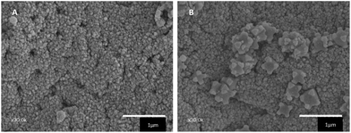
Fig. 11 shows the FE-SEM images of the copper films anodized under different hydrodynamic conditions.
Comparing Fig. 11A and the inset in Fig. 4A (anodization at 250 rpm and under stagnant conditions, respectively), it can be observed how the nanoparticle density is higher in the sample synthesized with 250 rpm respect to the sample anodized under stagnant conditions, indicating that the surface area of the active layer is bigger. Furthermore, nanoparticle diameters significantly decrease when anodization is carried out by stirring the Cu electrode, dropping from 0.91 nm at 0 rpm to 0.65 nm and 0.77 nm at 250 rpm and 500 rpm, respectively. A greater surface area together with smaller spheres’ diameters enhances the catalytic surface of the samples. Hence, a better photoelectrochemical performance might be achieved under hydrodynamic conditions, due to a major light absorption.
Fig. 11B shows that anodization performed under the highest hydrodynamic conditions (500 rpm) has a negative impact on the morphology of the nanostructure and, therefore, on its photoelectrochemical behavior. This is, at 500 rpm the surface of the nanostructure is more heterogeneous, since the nanoparticles start to form clumps of about 25–30 μm and these may hinder nanoparticles from light harvesting.
The XRD patterns of the copper oxide films anodized under different hydrodynamic conditions are shown in Fig. 12. From Fig. 12 it can be pointed out that there is no significant variation in the XRD patterns of 0 and 250 rpm samples. That is, peaks at 2θ = 36.5° and 61.5° associated with Cu2O are the only diffractions belonging to a copper oxide.
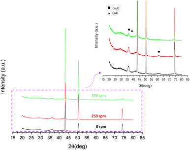 | ||
| Fig. 12 XRD patterns of copper oxide nanostructures after anodization in 70% (v/v) EG with a 0.05 M oxalic acid electrolyte under different hydrodynamic conditions (0 to 500 rpm). | ||
Nevertheless, when hydrodynamic conditions of anodization increase to 500 rpm the intensity of peaks at 2θ = 36.5° and 61.5° considerably decreases (see magnification Fig. 12), indicating that the fraction of Cu2O decreases. In addition, the magnification of the XRD pattern allows the detection of a new peak at 2θ = 38° for the sample anodized at 500 rpm, which belongs to CuO. Therefore, when the rotation speed of the electrode is increased to 500 rpm not only does copper(I) oxide become less present but the fraction of cupric oxide increases.
These results are confirmed by the Raman spectra displayed in Fig. 13.
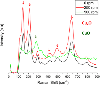 | ||
| Fig. 13 Raman spectra of CuOx nanostructures anodized in 70% (v/v) EG with 0.05 M oxalic acid under different hydrodynamic conditions (0 to 500 rpm). | ||
Fig. 13 shows that Raman spectra of the nanostructures anodized at 0 and 250 rpm present the typical peaks that correspond to Cu2O (145, 218, 412, 515 and 636 cm−1). When agitation increases to 500 rpm, these peaks become much smaller and peaks belonging to CuO are more intense (293 and 620 cm−1). Therefore, it can be concluded that as rotation speed exceeds 250 rpm, a larger fraction of CuO is engaged in the nanostructures and the presence of Cu2O decreases. Given that the presence of cuprous oxide increases the mobility of copper vacancies,31 having a lower proportion of it may have a negative effect on the photoelectrochemical performance of the nanostructures.
The samples prepared with oxalic acid under static (0 rpm) and dynamic conditions (250 and 500 rpm) have been also analyzed by transmission electron microscopy (Fig. 14). The images have been taken from the pieces of the nanostructures obtained by scratching the surface of the metallic support. This way, only the active oxidized material (copper oxide) is drawn although, due to the scratching, the nanostructures get broken.
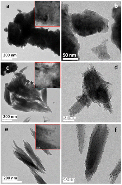 | ||
| Fig. 14 TEM images of CuOx nanostructures prepared in 70% (v/v) EG with 0.05 M oxalic acid under different hydrodynamic conditions: 0 rpm (a and b), 250 rpm (c and d) or 500 rpm (e and f). | ||
As can be seen in Fig. 14, the sample prepared under static conditions presents a compact structure. However, in the sample prepared at 250 rpm the main structure presents a feather-like shape although there are also a few small compact units (minorities). By increasing the magnification (Fig. 14d), it can be seen that the feather-like units are covered by scattered small nanoparticles, most of them in the 3–8 nm range. Similarly, for the catalyst treated at the highest rotation speed (500 rpm) feather-like units covered by small particles (3–9 nm) are mainly observed.
Additionally, selected area electron diffraction (SAED) analyses of the copper oxide samples have been undertaken to establish accurate crystallographic data in order to identify the nature of the crystalline phases (Fig. S8†). For the sample prepared under static conditions experimental d-spacings at 2.45, 2.13 and 1.28 A have been observed, which correspond to the (111), (200) and (311) planes, respectively, of Cu2O (JCPDS: 05-0667). In the case of the sample at 500 rpm, similar d-spacings have been detected, also indicating the presence of Cu2O. Moreover, the apparition in this sample of an additional ring at 2.53 A, suggests the presence of the more oxidized CuO phase (JCPDS: 45-0937).
Fig. 15 shows the DR-UV-Vis spectra of samples anodized in 70% (v/v) EG with 0.05 M oxalic acid in static (0 rpm) or under dynamic conditions (250 or 500 rpm).
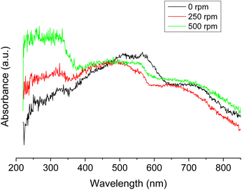 | ||
| Fig. 15 DR-UV-Vis spectra of CuOx nanostructures anodized in 70% (v/v) EG with 0.05 M oxalic acid under different hydrodynamic conditions (0, 250 or 500 rpm). | ||
Fig. 15 shows that the absorbance in the UV range increases when the rotation speed increases; moreover, the relative intensity between the band at 200–400 nm and that in the visible range between 400–650 nm is the lowest in the sample synthesized under static conditions. This info suggests that an increase in the rotation speed decreases the Cu+/Cu2+ ratio.
We want to mention that the determination of the energy band gap in these nanostructures is not straightforward as all the samples consist of mixtures of both CuO and Cu2O.
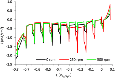
The photoelectrochemical response of the samples was studied by recording the photocurrent densities at different applied potentials with and without UV-light (see Fig. 16).
Fig. 16 shows that increasing the rotation speed to 250 rpm during anodization improves the photoelectrochemical behavior of the copper oxide nanostructures. This is easily attributed to a more homogeneous surface with more and smaller nanoparticles (Fig. 11A). In the same way, the worse photoelectrochemical response of the nanostructure anodized at 500 rpm is related to a lower presence of Cu2O (see Fig. 12 and 13), which decreases charge carrier mobility, and to lower light harvesting due to a more heterogeneous morphology of the nanostructures (see Fig. 11B).
The stability of the nanostructure anodized at 250 rpm is shown in Fig. S8.† There it can be observed that photocurrent values remain almost constant during 1 h applying −0.2 VAg/AgCl under UV-light irradiation.
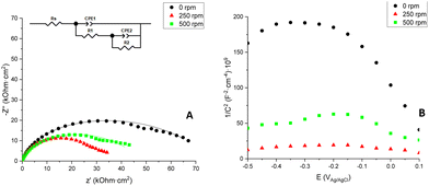
Electrochemical impedance spectroscopy (EIS) measurements were performed to study the resistance of the different photoelectrodes to charge-transfer processes. Fig. 17A shows the Nyquist plots for the CuOx nanostructures in the frequency range from 100 kHz to 1 mHz obtained at a potential of −0.2 V versus Ag/AgCl 3 M KCl.
In Fig. 17A, each Nyquist plot shows two semicircles, which correspond to two different regions of the Bode-module plots (Fig. S9†). The semicircle obtained at high and intermediate frequencies can be linked to the charge-transfer response of the oxide/electrolyte interface,35 which can give information about the active surface of the nanostructures. The second semicircle can be associated with a compact layer of copper oxide formed beneath the nanoparticles.36 In general, the impedance of the associated electrochemical process is proportional to the semicircle amplitude.
Observing Fig. 17A, the nanostructure with the largest semicircle is the one anodized under stagnant conditions (0 rpm), which means that this photoelectrode has the highest impedance. Both nanostructures anodized under hydrodynamic conditions present a smaller semicircle, the 250 rpm nanostructure having the smallest one. The total resistance offered by each nanostructure (RT) has been determined by the value registered at the lowest frequency in the Bode-module plot (Fig. S10†).
According to the morphology of this plot, the impedances of each sample can be determined by fitting the EIS results to an equivalent circuit with two parallel R–C time constants, as shown in Fig. 17A.
In this circuit, to account for the non-ideality of the system constant phase elements (CPEs) have been used instead of pure capacitors.37,38
For this circuit, RS represents the electrolyte resistance, R1-CPE1 belongs to the charge-transfer resistance at the active parts of the nanostructure/electrolyte interface39,40 and R2-CPE2 is related to the resistance offered by the compact layer of copper oxide.40–42Table 1 shows the values of RT and R1.
| CuOx_Ox70EG_5 min | R T (kOhm cm2) | R 1 (kOhm cm2) |
|---|---|---|
| 0 rpm | 67.70 | 27.27 |
| 250 rpm | 34.44 | 9.64 |
| 500 rpm | 43.89 | 15.00 |
Comparing the different samples obtained in this work, the resistance of the active parts of these nanostructures also decreases at 250 and 500 rpm indicating that spheres formed under stirring conditions have higher electrical conductivity than the spheres formed under stagnant conditions.
Hence, it can be inferred that hydrodynamic anodization improves the electron transfer and hole diffusion and this would result in a better photoelectrochemical performance.
The fact that the 500 rpm nanostructure exhibits a higher resistance than the 250 rpm one, however, makes it clear that excessive stirring is not beneficial for the process. The copper film anodized at 250 rpm presents the highest proportion of cuprous oxide compared to the rest of the nanostructures (see Fig. 12 and 13). Samples with a stronger Cu2O(111) orientation have registered lower resistance values.7,32,43 Therefore, the lower resistance of the 250 rpm anodized sample can be attributed to the higher presence of this copper oxide phase. In addition, the lower resistance of this nanostructure can be explained by the better electron transfer due to a more homogeneous surface (Fig. 11A), since clumps like the ones present in the 500 rpm nanostructure (Fig. 11B) can lead to bigger recombination of electron–hole pairs.
Moreover, these findings are confirmed by the Mott–Schottky plots displayed in Fig. 17B, where 1/C2versus the applied potential is represented and it is usually used to determine the carrier density of semiconductors. First, the negative slopes of these plots reveal that the formed Cu2O/CuO nanostructures are p-type semiconductors, with copper (Cu+/Cu2+) vacancies being the dominant charge carriers.1,25,44
The Mott–Schottky equation (eqn (3)) allows to calculate the acceptor density (NA) of each nanostructure from the slopes of the different plots, as well as the flat band potential (EFB) from the intercept of the straight line in the MS plots with the potential axis (Fig. 17B):
 | (3) |
![[thin space (1/6-em)]](https://www.rsc.org/images/entities/char_2009.gif) 45,46), E the applied potential, k the Boltzmann constant (1.38 × 10⁻²³ J K−1) and T the absolute temperature. The values of NA and EFB of each sample are summarized in Table 2.
45,46), E the applied potential, k the Boltzmann constant (1.38 × 10⁻²³ J K−1) and T the absolute temperature. The values of NA and EFB of each sample are summarized in Table 2.
| CuOx_Ox70EG_5 min | N A (cm−3) | E FB (VAg/AgCl) |
|---|---|---|
| 0 rpm | 2.01 × 10¹⁹ | 0.185 |
| 250 rpm | 2.68 × 10²⁰ | 0.321 |
| 500 rpm | 5.55 × 10¹⁹ | 0.193 |
In this case, acceptor density is related to the copper vacancies available on the active surface of the nanostructures. It is clear that anodization under hydrodynamic conditions increases the concentration of charge carriers. This can be attributed to an increase in the interfacial capacitance due to the larger surface area exposed to the electrolyte for the sample anodized at 250 rpm.47
A correlation can be observed between low resistances to charge transfer, high charge carrier densities and high photocurrents. This is that, a high density of copper vacancies would lead to a better mobility of electrons, increasing the conductivity of the nanostructure (lower resistance)44 and improving the photoelectrochemical performance of the photoanodes.
Moreover, Table 2 also shows the flat band potentials of each sample. The flat band potential is the potential that needs to be applied to the semiconductor in order to obtain a photoelectrochemical response (onset potential). The highest EFB is obtained from the CuOx nanostructure anodized at 250 rpm; therefore, less polarization of the system is required to achieve light response with this nanostructure. Furthermore, a more positive flat band potential decreases the recombination of electron–hole pairs, improving the photoelectrochemical performance of the nanostructure.15
Photoelectrochemical application of the optimized CuOx nanostructures: N2O reduction
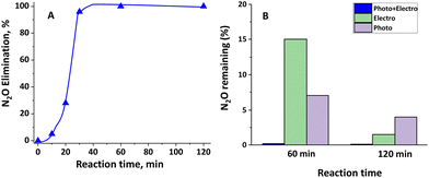
Fig. 18 reveals that the use of the photoelectrochemical approach using nanostructured copper oxide (sample anodized in 70% (v/v) EG with 0.05 M oxalic acid electrolytes at 250 rpm) as a photoelectrocatalyst leads to the almost complete removal of N2O after only 1 h. Following an initial period in which the removal efficiency was not elevated, a fast N2O decomposition was observed after 20 min and after 1 h only traces of nitrous oxide were detected.Fig. S11† shows the current density curve registered during the first hour of photoelectrochemical reduction, as the value was almost constant during the entire experiment.
To confirm the positive effect of anodizing under hydrodynamic conditions, this reaction was tested using the nanostructure synthesized at 0 rpm. After 2 h, only 68% of N2O elimination was reached.
In order to check the removal capacity of this combined solution, we tested separately the use of photocatalysis (with the same copper oxide sample) or the use of the same potential (electrocatalytic approach).
In these experiments, the removal efficiency was elevated although remarkably lower than the combined approach. Then, after 1 h, between 5–15% of N2O had not been eliminated with the separated approaches whereas with the combined approaches only ca. 0.2% was still remaining.
These results indicate that with facile anodization of copper oxide at 250 rpm, it is possible to synthesize stable nanostructures that can reduce N2O in short periods of time and that they can be employed in other photoelectrocatalytic applications.
Conclusions
In this study, CuOx nanostructures were synthesized by electrochemical anodization in different electrolytes. The use of hydrodynamic conditions and time during anodization was evaluated.According to the results, nanostructures anodized at 250 rpm for 5 minutes in ethylene glycol based electrolytes containing 0.05 M oxalic acid presented the best photoelectrochemical response. This could be attributed first, to the uniform nanosphere morphology with a feather-like phase covered by scattered small nanoparticles, second, to the formation of both CuO and Cu2O phases with the prevalence of the copper oxide in its reduced oxidation state, and third, to higher electrical conductivity with a higher number of copper vacancies and greater flat band potential.
This study presents an easy method for the synthesis of CuOx nanostructures that can be used in photoelectrochemical applications. In particular, the use of the sample as a photocathode in the reduction of N2O was tested for the first time, achieving a removal efficiency of almost 100% after 1 h using the photoelectrochemical approach.
Conflicts of interest
There are no conflicts to declare.Acknowledgements
The authors would like to acknowledge the Ministerio de Ciencia e Innovación-Agencia Estatal de Investigación through the projects PID2021-126235OB-C33 and TED2021-129555B-I00. The authors also thank the Generalitat Valenciana for CIAICO/2021/094, CIGRIS/2022/198, and CIGE/2022/166 and for the financial support (CIACIF/2021/010).References
- M. C. Huang, T. Wang, W. S. Chang, J. C. Lin, C. C. Wu, I. C. Chen, K. C. Peng and S. W. Lee, Appl. Surf. Sci., 2014, 301, 369–377 CrossRef CAS.
- M. Aloui, L. Mentar, A. Beniaiche and A. Azizi, J. Solid State Chem., 2022, 315, 123435 CrossRef CAS.
- J. Li, X. Jin, R. Li, Y. Zhao, X. Wang, X. Liu and H. Jiao, Appl. Catal., B, 2019, 240, 1–8 CrossRef CAS.
- P. Marathey, S. Khanna, B. Patel and A. Ray, Mater. Today: Proc., 2020, 28, 883–887 CrossRef CAS.
- P. J. M. Isherwood, A. Abbas, J. W. Bowers, B. Grew and J. M. Walls, Mater. Res. Innovations, 2014, 18, 95–98 CrossRef CAS.
- K. ur Rehman, A. Ullah Khan, K. Tahir, S. Nazir, K. Albalawi, H. M. A. Hassan, E. A. Alabbad, M. S. Refat, H. S. Al-Shehri and A. Mohammed Aldawsari, J. Mol. Liq., 2022, 360, 119453 CrossRef CAS.
- C. Ponchio and W. Srevarit, Chem. Pap., 2021, 75, 1123–1132 CrossRef CAS.
- D. W. Shoesmith, T. E. Rummery, D. Owen and W. Lee, J. Electrochem. Soc., 1976, 123, 790–799 CrossRef CAS.
- J. Ji and W. C. Cooper, J. Appl. Electrochem., 1990, 20, 818–825 CrossRef CAS.
- N. K. Allam and C. A. Grimes, Mater. Lett., 2011, 65, 1949–1955 CrossRef CAS.
- S. K. Kumar, S. Murugesan and S. Suresh, Opt. Mater., 2023, 135, 113304 CrossRef CAS.
- C. Wang, J. Cao, Z. Gao, S. Ji, H. Ma and Y. Wang, Mater. Chem. Phys., 2021, 264, 124470 CrossRef CAS.
- D. Gupta, S. R. Meher, N. Illyaskutty and Z. C. Alex, J. Alloys Compd., 2018, 743, 737–745 CrossRef CAS.
- Y. Yang, D. Xu, Q. Wu and P. Diao, Sci. Rep., 2016, 6, 35158 CrossRef CAS PubMed.
- T. H. Yin, B. J. Liu, Y. W. Lin, Y. S. Li, C. W. Lai, Y. P. Lan, C. Choi, H. C. Chang and Y. M. Choi, Coatings, 2022, 12, 1839 CrossRef CAS.
- T. H. Tran and V. T. Nguyen, Int. Scholarly Res. Not., 2014, 2014, 1–14 CrossRef PubMed.
- Y. Yecheskel, I. Dror and B. Berkowitz, Chemosphere, 2013, 93, 172–177 CrossRef CAS PubMed.
- C. Y. Chiang, Y. Shin, K. Aroh and S. Ehrman, Int. J. Hydrogen Energy, 2012, 37, 8232–8239 CrossRef CAS.
- World Meteorological Organization Global Ozone Research and Monitoring Project-Report No. 50 National Oceanic and Atmospheric Administration National Aeronautics and Space Administration United Nations Environment Programme World Meteorological Organization European Commission .
- S. A. Montzka, E. J. Dlugokencky and J. H. Butler, Nature, 2011, 476, 43–50 CrossRef CAS PubMed.
- L. Barrie and G. Braathen, WMO GREENHOUSE GAS BULLETIN: The State of Greenhouse Gases in the Atmosphere Based on Global Observations through 2021.
- S. Karthick Kumar, S. Murugesan and S. Suresh, Mater. Chem. Phys., 2014, 143, 1209–1214 CrossRef CAS.
- M. Balık, V. Bulut and I. Y. Erdogan, Int. J. Hydrogen Energy, 2019, 18744–18755 CrossRef.
- S. Jana, S. Das, N. S. Das and K. K. Chattopadhyay, Mater. Res. Bull., 2010, 45, 693–698 CrossRef CAS.
- J. Luo, L. Steier, M. K. Son, M. Schreier, M. T. Mayer and M. Grätzel, Nano Lett., 2016, 16, 1848–1857 CrossRef CAS PubMed.
- A. Nevin, J. L. Melia, I. Osticioli, G. Gautier and M. P. Colombini, J. Cult. Herit., 2008, 9, 154–161 CrossRef.
- R. L. Frost, Anal. Chim. Acta, 2004, 517, 207–214 CrossRef CAS.
- N. D. Khiavi, R. Katal, S. K. Eshkalak, S. Masudy-Panah, S. Ramakrishna and H. Jiangyong, Nanomaterials, 2019, 9, 1011 CrossRef CAS PubMed.
- A. El-Trass, H. Elshamy, I. El-Mehasseb and M. El-Kemary, Appl. Surf. Sci., 2012, 258, 2997–3001 CrossRef CAS.
- T. Baran, A. Visibile, M. Busch, X. He, S. Wojtyla, S. Rondinini, A. Minguzzi and A. Vertova, Molecules, 2021, 26 Search PubMed.
- K. Mizuno, M. Izaki, K. Murase, T. Shinagawa, M. Chigane, M. Inaba, A. Tasaka and Y. Awakura, J. Electrochem. Soc., 2005, 152, C179 CrossRef CAS.
- A. Paracchino, J. C. Brauer, J. E. Moser, E. Thimsen and M. Graetzel, J. Phys. Chem. C, 2012, 116, 7341–7350 CrossRef CAS.
- A. Paracchino, J. C. Brauer, J. E. Moser, E. Thimsen and M. Graetzel, J. Phys. Chem. C, 2012, 116, 7341–7350 CrossRef CAS.
- J. Yang, W. Li, J. Li, D. Sun and Q. Chen, J. Mater. Chem., 2012, 22, 17744–17752 RSC.
- R. M. Fernández-Domene, R. Sánchez-Tovar, B. Lucas-granados, M. J. Muñoz-Portero and J. García-Antón, Chem. Eng. J., 2018, 350, 1114–1124 CrossRef.
- R. M. Fernández-Domene, G. Roselló-Márquez, R. Sánchez-Tovar, B. Lucas-Granados and J. García-Antón, Sep. Purif. Technol., 2019, 212, 458–464 CrossRef.
- T. Zhu, M. N. Chong, Y. W. Phuan and E. S. Chan, Colloids Surf., A, 2015, 484, 297–303 CrossRef CAS.
- L. Li, S. Xiao, R. Li, Y. Cao, Y. Chen, Z. Li, G. Li and H. Li, ACS Appl. Energy Mater., 2018, 1, 6871–6880 CrossRef CAS.
- W. H. Leng, Z. Zhang, J. Q. Zhang and C. N. Cao, J. Phys. Chem. B, 2005, 109, 15008–15023 CrossRef CAS PubMed.
- S. Palmas, A. M. Polcaro, J. R. Ruiz, A. Da Pozzo, M. Mascia and A. Vacca, Int. J. Hydrogen Energy, 2010, 35, 6561–6570 CrossRef CAS.
- A. G. Muñoz, Electrochim. Acta, 2007, 52, 4167–4176 CrossRef.
- A. G. Muñoz, Q. Chen and P. Schmuki, J. Solid State Electrochem., 2007, 11, 1077–1084 CrossRef.
- G. Solomon, M. Lecca, M. Bisetto, M. Gilzad Kohan, I. Concina, M. M. Natile and A. Vomiero, ACS Appl. Energy Mater., 2023, 6, 832–840 CrossRef CAS.
- D. O. Scanlon, B. J. Morgan, G. W. Watson and A. Walsh, Phys. Rev. Lett., 2009, 103, 096405 CrossRef PubMed.
- E. Szaniawska, I. A. Rutkowska, M. Frik, A. Wadas, E. Seta, A. Krogul-Sobczak, K. Rajeshwar and P. J. Kulesza, Electrochim. Acta, 2018, 265, 400–410 CrossRef CAS.
- A. A. M. Farag, A. Ashery and M. A. Salem, Superlattices Microstruct., 2019, 135, 106277 CrossRef CAS.
- R. M. Fernández-Domene, R. Sánchez-Tovar, B. Lucas-Granados and J. García-Antón, Appl. Catal., B, 2016, 189, 266–282 CrossRef.
Footnote |
| † Electronic supplementary information (ESI) available. See DOI: https://doi.org/10.1039/d3dt02017g |
| This journal is © The Royal Society of Chemistry 2023 |

