 Open Access Article
Factors influencing self-trapped exciton emission of low-dimensional metal halides
Ying
Han†
ab,
Xiaohua
Cheng†
 ab and
Bin-Bin
Cui
 *abc
*abc
aAdvanced Research Institute of Multidisciplinary Science, Beijing Institute of Technology (BIT), Beijing 100081, P. R. China. E-mail: cui-chem@bit.edu.cn
bSchool of Chemistry and Chemical Engineering, BIT, Beijing 100081, P. R. China
cSchool of Materials Science and Engineering, BIT, Beijing 100081, P. R. China
First published on 18th November 2022
Abstract
Organic–inorganic hybrid metal halides (MHs) are widely used in the field of photoelectricity due to their excellent structure and photoelectric tunability. When separating inorganic metal halides by larger organic cations in crystals, multiple low-dimensional MHs (LDMHs) at the molecular level can be constructed, including two-dimensional (2D) layers, one-dimensional (1D) chains, and zero-dimensional (0D) clusters assembled by octahedral metal halide units. These LDMHPs exhibit significantly different luminescence properties from 3D MHs, which stem from the radiative recombination of self-trapped excitons (STEs) or the defect states. Along with the structure dimensions, the degree of intrinsic and instantaneous structure distortions greatly affects the STE broadband emission of LDMHs. Furthermore, molecular engineering such as the choice of organic cations, electron–phonon coupling effect, external temperature and pressure, and metal ion doping can greatly change the luminescence properties of LDMHs. Herein, we summarize and discuss the factors influencing the STE emission of LDMHs for a better understanding and to prospect the development of LDMHs in future.
1. Introduction
Organic–inorganic hybrid metal halides (MHs) have been widely applied in optoelectronic devices for their unique, multiple, and tunable structures,1 as their dimensions and intrinsic structures can be regulated by rational design with components.2 As shown in Fig. 1, replacing methylammonium (MA+), formamidine (FA+), and/or cesium (Cs+) in three-dimensional (3D) metal halides by larger organic cations in size can build multiple low-dimensional MHs (LDMHs) at the molecular level,3 such as two-dimensional (2D) layers, one-dimensional (1D) chains, and zero-dimensional (0D) metal halide octahedral clusters.4 LDMHs have opened a new frontier in photodetector,5 scintillator,6 laser,7 single component phosphor,8 and light emitting diode (LED) devices9 for excellent luminescence and high photoluminescence quantum efficiency (PLQE).10 Traditional 3D lead halide perovskites usually show narrow emissions.11 On the contrary, LDMHs exhibit typical luminescent properties of large Stokes shift and broadband emission, which is usually attributed to the radiative recombination of self-trapped excitons (STEs).12 The soft nature of the LDMHs make ultrafast structural distortion easier upon optical excitation.13 The formation of STEs is due to the strong electron–phonon coupling in the distortion-induced lattices, which generates small polarons binding the excitons under excitation.14 While the luminescence mechanism of the broadband emission in regular 100-oriented 2D MHs is still under debate. In addition to STE states emission, the defect-induced broadband emission has recently been reported in (BA)2PbBr415 and (PEA)2PbI416 2D perovskite crystals.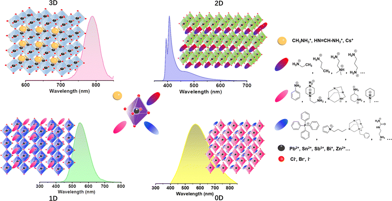 | ||
| Fig. 1 Typical structures of 3D, 2D, corrugated 2D, 1D, and 0D MHs and their typical photoluminescence spectra, respectively. | ||
Generally, the degree of the intrinsic inter-octahedral and/or individual intra-octahedral distortions are related to the broadband emission of the self-trapping states.17 Inter-octahedral distortion can be divided into out-of-plane distortion and in-plane distortion. The photoluminescence (PL) intensity of the broad emission increases linearly with increasing out-of-plane distortion degree,18 and the lead-halide octahedral intra-octahedral distortion has a linear relationship with the full width at half-maximum (FWHM) of the PL emission, showing the dependency of STE emission on the structure distortion.19 In addition, instantaneous structure distortion after being excited has a great influence on STE states and emission.20 Structure distortion can be regulated by reasonably choosing chemical compositions, which influence the photoelectric properties of LDMHs. Molecular engineering, such as the choice of organic cations, can also directly regulate the photoluminescence characteristics of LDMHs.21 The energy level of organic cations relative to that of inorganic frameworks can be regulated by adjusting organic molecules, which result in different types of emissions with different mechanisms.22 It is worth mentioning that the vibration of organic cations that are not isolated from the inorganic cage and the regulation of organic cations can effectively tune the electron–phonon coupling strength.23
Furthermore, the configuration of some LDMHs that changes with ambient temperature and pressure will produce structure transition and greatly change the photophysical and photoelectric properties of LDMHs.11 For example, pressure-induced emission (PIE) has been found in some LDMHs, such as 1D EAPbI3,24 C4N2H14SnBr4,25 and 2D (PEA)2PbBr4,26 (BA)4AgBiBr827 perovskite crystals. In addition, doping metal ions can tune the luminescence properties and efficiently enhance the luminescence of LDMHs. For example, divalent Mn2+ can introduce intermediate energy level emission and greatly improve PLQE.28 Other doping metal elements in LDMHs have also been investigated, such as Sb3+,29 Bi3+,30 and Sn2+.31
In conclusion, the structure distortion, molecular engineering of organic cations, electron–phonon coupling strength, external temperature and pressure, and metal ion doping will greatly affect the STE broadband emission of LDMHs. However, the generalization and summarization of the role of these factors on self-trapped excitons of LDMHs are still not systematic enough. In this work, we mainly introduce and discuss these factors influencing the STE emission of LDMHs, which will help us to better design LDMH materials with specific and photoelectric functions.
2. The STE broadband emission mechanism
Unlike 3D metal halide perovskites and most regular 100-oriented 2D structures with small Stokes shifts and narrow FWHM, 0-1D MHs,32 110-oriented corrugated 2D MHs,12a,b,33 some distorted 100-oritented 2D MHs12c,33,34 usually have broadband emissions with large Stokes shifts, and usually white emissions covering the entire spectrum at room temperature. Here, the difference lies in that the 3D perovskite material under excitation generates large-area polarons35 (Fig. 2(a)), which exhibit long-range distortion of the lattice. However, when the LDMHs are excited, Pb–X bonds are easily deformed to generate small polarons and trap excitons.36 As shown in Fig. 2(b), when the Pb–Pb bonds are shortened, the photogenerated electrons are captured at the Pb–Pb site, and the Pb–Pb dimer couples with photogenerated electrons to form Pb23+. Similarly, when the X–X bands are shortened, holes are trapped to form X2− and when Pb–X bonds are shortened, holes are located on a single Pb atom, resulting in the formation of Pb3+ centers.38 Therefore, an intermediate energy STE states for trapping electron and holes is introduced into the forbidden band39 (Fig. 2(c)). The STE level has a wide energy distribution, which results in broadband emission with a large Stokes shift of LDMHs.40 It is worth mentioning here that for the 0D MHs, the single lead-halide octahedrons are completely isolated by organic cations (Fig. 2(d)). The excitons are completely confined to the isolated individual octahedron and there is no coupling effect.41 The mechanism of broadband emission from 0D MHs is shown in Fig. 2(e), which a significant change in the charge distribution compared to the ground state upon excitation causes changes in the bond length and bond angle of the individual octahedron, in turn leading to excited-state structural reorganization.37 The reorganized excited states have wide energy distribution energy related to the degree of structural distortion, which results in the broadband emission of 0D MHs.42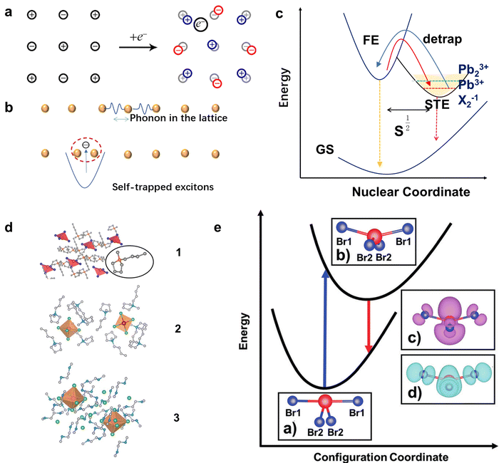 | ||
| Fig. 2 (a) Schematic diagram for the formation of large polarons in the lattice of a 3D material excited by light. Reproduced with permission.36 Copyright 2018 American Chemical Society. (b) Schematic diagram of the Pb–Pb dimer couples with photogenerated electrons to form Pb23+ in LDMHs. (c) Graphs of low-dimensional perovskite excitons self-trapping (blue) and detrapping (red) (GS = ground state, FE = free exciton state, STE = self-trapped exciton state, pink, and black downward arrows indicate FE and STE photoluminescence, respectively). (d) The 0D structures are completely isolated by organic cations. Reproduced with permission.37 Copyright 2018 Wiley-VCH. (e) Configuration coordinate diagram of the large Stokes displacement caused by the deformation of the excited state structure of 0D structures. Reproduced with permission.37 Copyright 2018 Wiley-VCH. | ||
Furthermore, the origin of the broadband emission in 100-oriented 2D MHs is still controversial, and there are two mechanisms. In addition to the explanation of the broadband emission by the STE mechanism, some recent studies and evidence suggest that such emission may also be caused by the defect states rather than STE states. For example, Zhang et al.16 showed that the broadband emission intensity of (PEA)2PbI4 can be adjusted by tuning the concentration of excess iodine during crystal growth. As shown in Fig. 3(a), the crystal 0.157 I-PEPI exhibits yellowish emission, which is distinct from the green emission of typical 0I-PEPI crystals. 0I-PEPI show a sharp emission, while 0.157I-PEPI show a dominant broadband emission (Fig. 3(b)). The broadband emission shows an increasing ratio with increasing iodine ion concentration (Fig. 3(c)). In this case, the authors suggest that broadband emission originates from iodine interstitials. In addition, Park et al.15 found that the PL intensities of broadband emission in the (BuA)2PbBr4 crystal were proportional to the thickness (Fig. 3(d)). They predicted that the broadband emission may originate from defect radiative recombination, i.e., the organic cation vacancies generated by intercalated water molecules (Fig. 3(e)).
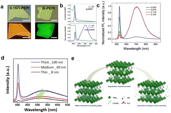 | ||
| Fig. 3 (a and b) Optical micrograph and corresponding fluorescence images under excitation for 0.157I-PEPI and 0I-PEPI crystals.16 (c) UV-vis Abs and PL spectra of 0I-PEPI flakes and 0.157I-PEPI flakes. Reproduced with permission.16 Copyright 2019 American Chemical Society. (d) PL spectra of the OHP depending on the thickness.15 (e) Schematic of the water-assisted degradation mechanism in (BuA)2PbBr4 microsheets. Reproduced with permission.15 Copyright 2019 American Chemical Society. | ||
Kahmann et al. made a distinction between the two mechanisms, as shown in Fig. 4(a), wherein STEs are formed by transient lattice deformation after excitation, and therefore, only the above-gap excitation can lead to STE luminescence. However, the defect states can also be excited directly by excitation energies lower than the bandgap.43 They performed the PL spectrum of PEA2PbI4 excited by below-bandgap photons. As shown in Fig. 4(b), identical broadband emission using excitation energy from 2.07 to 2.48 eV proves that the broadband emission originates from defects. Furthermore, Yin et al.44 experimentally and theoretically demonstrated that the broadband emission in PEA2PbI4 originates from the iodine vacancies defect luminescence centers (Fig. 4(c)). As shown in Fig. 4(d), for 2D PEA2PbI4 crystals treated by excess PEAI, the intensity of broadband emission was largely reduced as the PEAI treatment plays a key role in the passivation of I vacancies of the single crystals. It is worth mentioning that for the tin-based 100-oriented 2D MHs, it is easier to produce strong STE emission rather than defect-induced emission. For example, Deng et al.45 reported the 2D tin halide perovskite, which exhibited STE emission with a large Stokes shift and broad bandwidth. It displayed a high PLQE of near-unity in the solid-state and showed excellent stability.
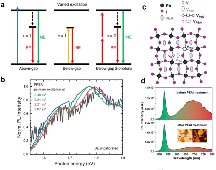 | ||
| Fig. 4 (a) Two-photon excitation scales of above-gap and below-gap energy.43 (b) The broad emission can be excited using below-gap photons. Reprinted with permission.43 Copyright 2020 Springer Nature. (c) Schematic illustration of point defects (VI, VPEA, VPbI2, and VPEAI) of PEA2PbI4.44 (d) PL spectra of the PEA2PbI4 before and after PEAI treatment. Reprinted with permission.44 Copyright 2020 American Chemical Society. | ||
In our scenario, the broadband emission reported to be from self-trapping states need to be verified by further post-treatments, such as acetone46 or cationic salts solution44 ultrasound. In addition, the ratio of organic amine to lead oxide (PbO) needs to be changed during synthesis, and the single crystals grown can be recrystallizated to eliminate defects.
3. Factors influencing STE broadband emission
3.1. Structure distortion
To date, materials with broadband emission are mostly 1D,47 0D,32b,48 and corrugated 110-oriented 2D MHs.12 Most 100-oriented 2D perovskites show emission with a narrow peak, and a few distorted 100-oriented 2D perovskites exhibit STE broadband emission.34,49 Previous papers consistently reported that the STE emission of 100-oriented perovskites are related to the degree of inter-octahedral distortion of the inorganic layer and intra-octahedral distortion of individual octahedrons.49,50 The inter-octahedral distortion (Fig. 5(a)) can be divided into two types—out-of-plane distortion (Fig. 5(b)) and in-plane distortion (Fig. 5(c)).18 The in-plane distortion is that the Pb–Br–Pb bond angle parallel to the 2D layer deviates from 180 degrees, which is recorded as θin, Din = 180° − θin. Out-of-plane distortion refers to distortion perpendicular to the direction of the layer, which is denoted as θout, Dout = 180° − θout. It has recently been verified that the emission intensity of 100-oriented 2D structures is directly related to out-of-plane distortion. As shown in Fig. 5(d), the increasing Dout correlates linearly with the increasing intensity of STE broadband emission.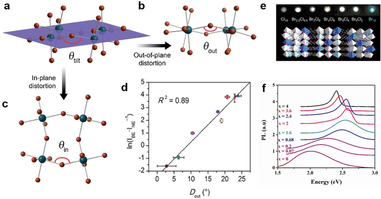 | ||
| Fig. 5 (a) Schematic diagram of the octahedral tilt decomposition into two parts: out-of-plane distortion (b) and in-plane distortion (c). (d) Relationship between ln(IBE/INE) and Dout. Reproduced with permission.18 Copyright 2017 The Royal Society of Chemistry. (e) The mixed halogen EA4Pb3Br10−xClx (x = 0, 2, 4, 6, 8, 9.5, 10) crystals. Reproduced with permission.53 Copyright 2019 American Chemical Society. (f) PL of (C6H11NH3)2[PbBr4−xIx] varies with the content of I. Reproduced with permission.54 Copyright 2017 Elsevier B.V. | ||
As for the intra-octahedral distortion of individual octahedrons, the calculation formula is as follows
In addition, some other researchers regulated the structure distortion by regulating the halogen to achieve broadband white light emission.52 For example, EA4Pb3Cl10 with a large distortion shows broadband white emission, while EA4Pb3Br10 with a small distortion shows narrow blue emission.53 By further adjusting the Cl/Br ratio for EA4Pb3Br10−xClx (x = 0, 2, 4, 6, 8, 9.5, 10), they found that two compounds (x = 8 and 9.5) have more optimized white emissions than pure EA4Pb3Cl10 (Fig. 5(e)). Aymen Yangui et al.54 realized white-light emission from the mixed 2D hybrid perovskites (C6H11NH3)2[PbBr4−xIx] and studied the FWHM of PL increasing with the bromine content (Fig. 5(f)), which was excellently correlated with the change in the angular distortion in inorganic octahedral PbX6 (X = I/Br).
It is worth mentioning that instantaneous structure distortion under excitation also has a great influence on STE emission. For example, Ye et al.20 reported that broadband emission shows strong dependence on the molecular conformational of organic cations. They synthesized a series of 2D perovskites with different lengths ([CH3(CH2)n−1NH3]2PbI4, n = 4, 6, 8, 10, 12, 18). With the increase in the cationic chain length, the chain distortion of organic cations is easy under excitation, which induces polaron formation and charge-carrier trapping. As shown in Fig. 6(a), as the organic cations chain length increases, the charge-carrier mobility initially increases (n ≤ 6) and then decreases (n ≥ 6). As illustrated in Fig. 6(b), there is a relationship between the low charge-carrier mobility and broadband emission. After the free carriers are relaxed to free excitons, the self-trapped excited states with different energies will gradually form in the bandgap. As shown in Fig. 6(c), the ratio of the PL intensity of broadband emission to narrow emission (IBE/INE) decreased with increasing temperature. Fig. 6(d) plots the IBE/INE ratio at 80 K against the organic cations chain length with different n values. It was found that the ratio increases with increasing organic cation chain length (n ≥ 6), which suggests that instantaneous organic chain distortion is conducive to broadband emission.
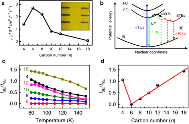 | ||
| Fig. 6 (a) Out-of-plane charge-carrier mobility varies with n value curves. (b) Schematic of the adiabatic potential energy curves of the ground state (G), free-exciton state (FE), free-carrier state (FC), and various self-trapped excited states (STEs). The vertical dashed line shows possible nonradiative decay processes of the FE and STEs. (c) The IBE/INE ratio of six samples as a function of temperature ranging from 80 K to 150 K. (d) The IBE/INE ratio at 80 K is plotted against the alkyl chain length of organic cations. Reprinted with permission.20 Copyright 2020 Springer Nature. | ||
3.2. Molecular engineering
These LDMHs structures can be regulated by the size of organic cations.55 For example, for the 2D perovskite (RnNH3)2MX4 and (NH3RnNH3)MX4 constructed by monoamine and diamine organic cations, as shown in Table 1, when n = 1, methylamine cation constructs traditional 3D perovskites,56 and when n ≥ 2, 2D perovskites are formed.53 While for (NH3RnNH3)MX4, when n ≥ 4, regular 100-oriented 2D perovskites can be formed due to the sufficiently long diamine organic cations.57 As shown in Fig. 7(a) and Table 1, in the formation of butylenediamine (n = 4), propylene enediamine (n = 3), and ethylenediamine (n = 2), as the length of the amine chain is reduced, the layered perovskite changes from a flat layer to a distorted layer, then when n = 2, the layer is broken up to construct a 1D structure, resulting in emission transition from a narrow emission to a STE broadband emission.58 In addition, the cation length also influences the connection styles of the inorganic skeleton. As shown in Fig. 7(b), PMA and PEA organic cations constructed the corner-sharing 2D structures, while the longer PPA and PBA cations constructed corner-sharing and face-sharing coexistent 2D structures.59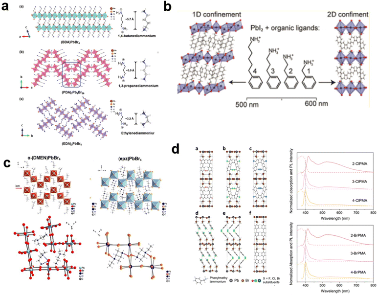 | ||
| Fig. 7 (a) Views of the structures of 2D and 1D perovskites. Reproduced with permission.58 Copyright 2020 Wiley-VCH. (b) The 2D structures with corner-sharing, corner-sharing, and face-sharing coexistence. Reproduced with permission.59 Copyright 2016 American Chemical Society. (c) Structures of corrugated 2D perovskite and hydrogen bonding diagram. Reproduced with permission.19 Copyright 2017 American Chemical Society and60 Copyright 2018 American Chemical Society. (d) The 2D perovskites with halogen-substituted organic cations and their PL spectrum. Reproduced with permission.61 Copyright 2021 Springer Nature. | ||
Furthermore, by the hydrogen bonding force of organic cations, corrugated 110-oriented 2D perovskites can be constructed. The H atoms on the primary and secondary amines of organic cations forms hydrogen bonding with bromine atoms. Therefore, the inorganic layer can be folded ∼90° to form a corrugated structure (Fig. 7(c)), such as (N-MEDA)[PbBr4].12c α-(DMEN)PbBr4,19 and (epz)PbBr4.60 Cui et al.32b also reported the transition from the 1D to 0D structure by regulating the hydrogen bonding, and the dimension reduction from 1 to 0D increased the PLQE five times from the STE states. Recently, Xing et al.61 reported the atomic substitution strategy to facilitate the formation of STEs in 2D perovskites. As shown in Fig. 7(d), perovskite crystals are synthesized by halogen-substituted phenyl molecules. The halogen substituent can promote exciton self-trap, resulting in STE broadband emission.
Engineering organic cations can not only tune the intrinsic structures of LDMHs but also play a key role in determining their optical features. Different types of emission can be achieved by regulating the energy levels of different organic cations. The relative level of the LUMO, HOMO energy level of organic cations, and the CBM and VBM of the inorganic framework can be regulated by adjusting organic molecules. For example, Dou et al.22 demonstrated that the organic and inorganic building blocks of hybrid perovskite materials can be manipulated in a modular fashion to produce widely tunable single crystalline quantum wells. As shown in Fig. 8, there are different types of energy transfer, type 1 is the emission type of most perovskite materials. The energy level of inorganic skeleton is below that of organic molecules, thus showing efficient narrow band emission of inorganic skeleton, and the (ii), (iii), (iv) type realized that the inorganic layer transfers energy to the organic cations, which results in the broadband emission from the organic molecules of these perovskite materials.
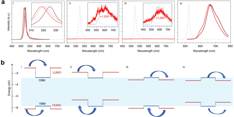 | ||
| Fig. 8 (a) Corresponding diagram (i), (ii), (iii), (iv) emission spectra of four different types of quantum traps, where the low-energy broad peak comes from organic molecules. (b) Four types of quantum wells constructed by the relative changes in the LUMO HOMO energy level of organic molecules and the CBM and VBM of inorganic frameworks (VBM, valence band maximum; CBM conduction band minimum; HOMO, highest occupied molecular orbital; LUMO, lowest unoccupied molecular orbital). Reprinted with permission.22 Copyright 2020 Springer Nature. | ||
For some LDMHs, white-light emission can be attributed to the synergetic effects of the self-trapped excitons and organic component.62–64 For example, Luo et al.65 reported a white-light emissive 1D hybrid perovskite, C5H14N2PbCl4·H2O (Fig. 9(a)), and they proved that the white-light emission was derived from the synergy of the organic part and self-trapped exciton. As shown in Fig. 9(b), the material exhibits different emission characteristics at different excitation wavelengths, and there are two emission peaks when excited by 344 nm: the narrow emission located at 412 nm is from the C5H14N2Cl2 organic part and the broad emission centered at 617 nm is from self-trapped excitons of the inorganic skeleton. We can see from the photoluminescence photographs and CIE chromaticity coordinates that the broadband white emission is produced by the combination of cations with blue light and inorganic components with yellow light. Guo et al.66 also synthesized two crystalline hybrids (H2DABCO)(Pb2Cl6) and (H3O)(Et2-DABCO)8(Pb21Cl59); the structures are shown in Fig. 9(c). These materials also exhibit the cooperative luminescence of the organic and inorganic part (Fig. 9(d)).
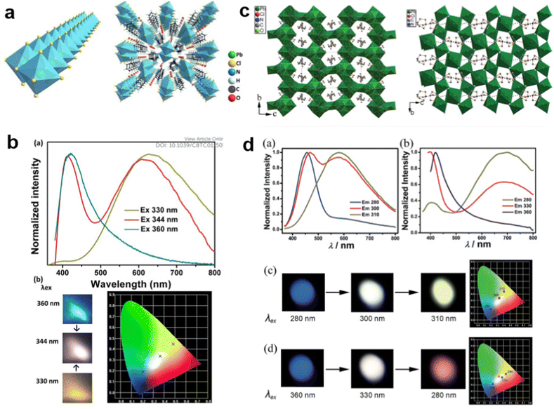 | ||
| Fig. 9 (a) The structure of 1D hybrid perovskite C5H14N2PbCl4·H2O.65 (b) Emission spectra and photoluminescence photographs corresponding CIE chromaticity coordinates of C5H14N2PbCl4·H2O excited by different energies. Reprinted with permission.65 Copyright 2013 The Royal Society of Chemistry. (c) The structures of hybrid perovskites (H2DABCO)(Pb2Cl6) and (H3O)(Et2-DABCO)8(Pb21Cl59).66 (d) Emission spectra and photoluminescence photographs corresponding CIE chromaticity coordinates of (H2DABCO)(Pb2Cl6) and (H3O)(Et2-DABCO)8(Pb21Cl59) excited by different energies. Reprinted with permission.66 Copyright 2015 The Royal Society of Chemistry. | ||
3.3. The electron–phonon coupling effect
It is worth mentioning that the regulation of organic cations greatly affects the electron–phonon coupling of the materials,67 which has a significant impact on PLQE,23 FWHM,68 PL emission peak,69 hot-carrier cooling,70 STE broadband emission,71etc. The organic cations affect the rigidity of perovskite materials, which further significantly affects the electron–phonon coupling strength. Sargent's group23 compared the 2D perovskites PEA2PbBr4 and BA2PbBr4 (Fig. 10(a)), and PEA2PbBr4 has higher crystal rigidity due to the lower conformational freedom of organic cations, which leads to weak electron–phonon coupling strength. Fig. 10(b) shows the Raman spectra of PEA2PbBr4 and BA2PbBr4; the BA2PbBr4 Raman spectrum is several times more intense than that of BA2PbBr4, indicating the stronger electron–phonon coupling strength, which enhances the non-radiative recombination rates, resulting in very low PLQE, while the PEA with large rigidity has a high PLQE of 79%. In addition, the cation stacking pattern affects the microstrain, which has been reported by Du et al.72 As shown in Fig. 10(c), the FWHM of the XRD peaks increased monotonously with decreasing cation rigidity. A large microstrain leads to strong electron–phonon coupling, which is responsible for the widening of the emission peak (Fig. 10(d)). The 2D perovskite crystals usually shows dual peaks, such as PEA2PbBr4, OA2PbBr4, and BA2PbBr4. Many reports consistently proved that the low-energy peak is from the bulk phase, and the high-energy peak is from a distorted surface phase. Recently, F. Nogueira et al.69 studied the dual bands emission of the well-known (BA)2PbI4 (Fig. 10(e)). They found the phonon energy that is quite consistent with the vibration of organic cations in the Raman and infrared spectra (Fig. 10(f)). These vibrational modes transformed from the organic cations to the inorganic layer, resulting in strong electron–phonon coupling and dual band emission.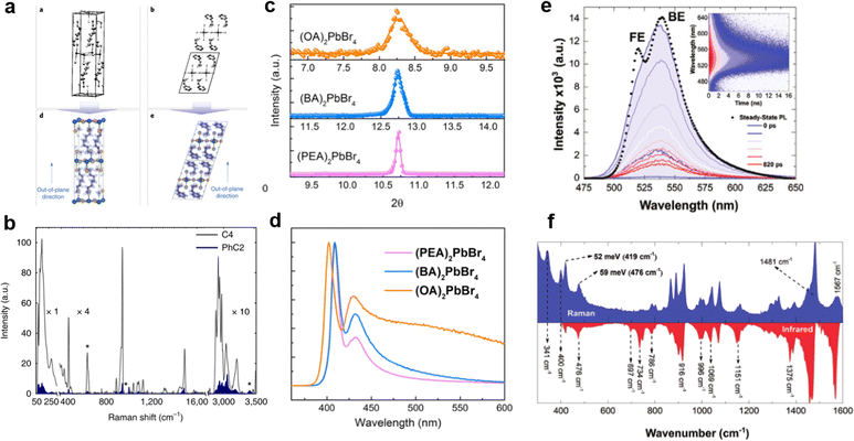 | ||
| Fig. 10 (a) The structure of 2D perovskites BA2PbBr4 and PEA2PbBr4.23 (b) Raman spectrum of BA2PbBr4 and PEA2PbBr4. Reprinted with permission.23 Copyright 2018 Springer Nature. (c) XRD spectra in the (004) planes of the single crystals with different organic cations.72 (d) PL spectra of the single crystals with different organic cations. Reprinted with permission.72 Copyright 2020 American Chemical Society. (e) The time-resolved PL spectra reconstruction at different times.69 (f) Raman and attenuated total reflectance infrared spectra. Reprinted with permission.69 Copyright 2020 Wiley-VCH. | ||
In addition, the hot carrier cooling rate is closely related to the electron–phonon coupling strength. The cooling process of hot carriers is shown in Fig. 11(a); immediately upon photoexcitation, the hot charge carriers are injected into all the perovskite QWs and then cool to the band edge states. The strong electro-acoustic coupling effect is beneficial for accelerating carrier cooling and decreasing the cooling rate to a ‘hot phonon bottleneck effect’.70c Therefore, for the perovskite material, the electron–phonon coupling strength can be changed by regulating the cations, thereby affecting the cooling rate of hot carriers. For example, Zhang et al.73 studied the different impacts of spacer layer BA cations confined by the 2D framework and MA cations confined by 3D framework have charge carrier dynamics in the two systems. They found that 2D (BA)2(MA)Pb2I7 has a faster hot carrier decay rate than that in 3D MAPbI3 due to the stronger nonadiabatic couplings (Fig. 11(b)). Yin et al.74 also studied the hot carrier cooling process of three single-crystal 2D hybrid perovskite systems (Fig. 11(c)). As shown in Fig. 11(d), they found that (EA)2PbI4 with weak electron–phonon coupling has a longer hot carrier cooling time compared to that of (AP)2PbI4 and (PEA)2PbI4. Therefore, reducing the vibrational coupling between the organic cations and the inorganic framework by changing the functional groups of the organic spacer cations has the potential to slow down the hot carrier relaxation and increase the carrier lifetime, thereby improving the PCE of solar cells.
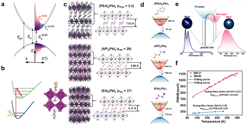 | ||
| Fig. 11 (a) The schematic representation showing the carrier cooling process. Reprinted with permission.70c Copyright 2015 Springer Nature. (b) The faster hot-carrier decay rate in 2D (BA)2 (MA)Pb2I7. Reprinted with permission.73 Copyright 2018 American Chemical Society. (c) Schematic illustrations of (PEA)2PbI4, (AP)2PbI4, and (EA)2PbI4 single crystals. (d) Hot electron relaxation and electron–hole pair recombination processes after high-energy excitation. Reprinted with permission.74 Copyright 2018 American Chemical Society. (e) Absorption and emission spectra for the bulk (C7H7N2)2PbBr4 and (C7H7N2)2PbCl4 crystals at RT. (f) The FWHM of the broadband emission peak vs. temperature was plotted to obtain the Huang–Rhys factor S. Reprinted with permission.75 Copyright 2022 American Chemical Society. | ||
Furthermore, the formation of an STE depends strongly on electron–phonon coupling to induce small polarons in the local lattice.14 Recently, Chen et al.75 reported the two 100-oriented 2D perovskites (C7H7N2)2PbX4 (X = Cl, Br) with two different halogens. Interestingly, the two perovskite crystals show different emission mechanisms even with a similar monolayer crystal structure, which are almost deformation-free in the inorganic octahedral framework (Fig. 11(e)). As shown in Fig. 11(f), the halogen substitution from Cl− to Br− results in a 10-fold enhancement of the electron–phonon coupling that affects the dynamics of STE. (C7H7N2)2PbBr4 crystals with weak electron–phonon coupling (S = 13) produce deep blue photoluminescence at RT. In contrast, due to the strong electron–phonon coupling with S = 181, (C7H7N2)2PbCl4 exhibits an STE-derived broadband white emission at RT, which is almost the highest value among the bulk semiconductor materials we know so far.
The Huang–Rhys factor (S) is often employed to quantify the strength of electron–phonon coupling.76 It has been reported that materials with self-trapping emission usually have large S, as shown in Table 2.
| Compounds | Huang–Rhys factor (S) |
|---|---|
| (C7H7N2)2PbCl475 | 181 |
| (C7H7N2)2PbBr475 | 13 |
| Cs4SnBr642 | 107 |
| (NMEDA)PbBr442 | 82 |
| Cs2NaInCl677 | 80 |
| Cs3Bi2I978 | 79.5 |
| C4N2H14PbBr442 | 57 |
| Rb3Sb2I978 | 50.4 |
| Cs3Sb2I978 | 42.7 |
| Cs2AgInCl679 | 41 |
| Cs2AgBiBr680 | 11.9 |
| MAPbI381 | 5–20 |
| CsPbBr382 | 0.55 |
| CsPbX3, X = Br, Cl, I83 | 0.075–0.247 |
| (PEA)2PbI484 | 0.44–2.49 |
| (BA)2(MA)n–1PbnI3n+185 | 1.24 |
| NaCl86 | 42 |
| AgCl/Br87 | 22 |
| MgCl288 | 4 |
| MnCl288 | 2.4 |
| CdCl288 | 4.5 |
| CdSe89 | 1 |
| ZnSe90 | 0.3 |
| Cs2NaYCl691 | 6.86 |
| K2NaScF691 | 3.50 |
| K2NaGaF691 | 3.12 |
3.4. Temperature and pressure
External factors such as temperature and pressure can effectively adjust the structure and photoelectric properties of LDMHs. Perovskite materials usually undergo phase transition caused by the configurational changes of organic cation when the temperature changes,92,93 which further affect the photoelectric properties. For example, as the temperature increases, the organic cation arrangement becomes disordered, and the point of disorder is called the melting temperature11 (Fig. 12(a)). The disordered arrangement of organic cations results in abrupt changes in the lattice parameters along the organic direction and changes in the spacing of 2D layered structures. Aurang Zeb et al.94 reported an organic–inorganic hybrid 1D perovskite crystal has an obvious phase transformation at about Tc = 202 K and remarkable change of dielectric response (Fig. 12(b)), which is caused by the ordered–disordered transition of organic cations. It proves that the crystal lattice-related phase transition is related to the conformation of the alkylammonium chain.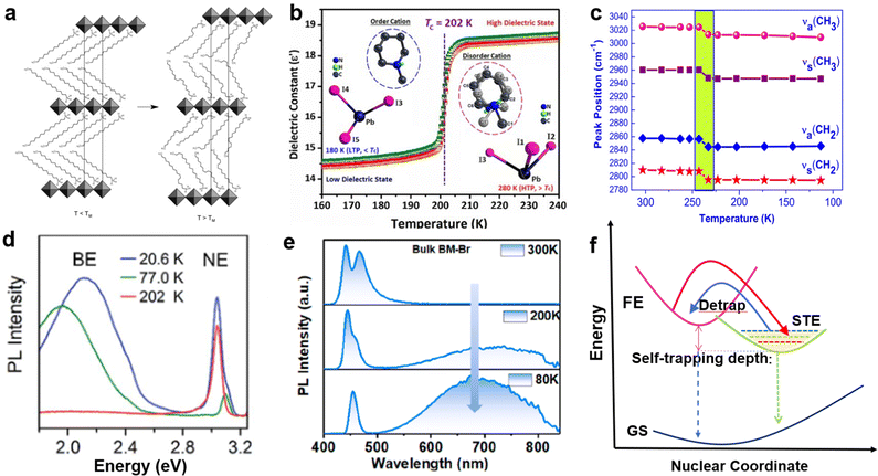 | ||
| Fig. 12 (a) Schematic depiction of the melting transition in (CnH2n+1NH3)2PbI4 compounds. Reproduced with permission.11 2019 American Chemical Society. (b) Phase transition and dielectric response of 1D perovskite structural phase transition induced by temperature. Reproduced with permission.94 Copyright 2018 The Royal Society of Chemistry. (c) Peak position of the methylene C–H stretching at different temperatures between 303 K and 113 K. Reproduced with permission.95 (d) The broadband emission appears at low temperature in 100-oriented 2D perovskite. Reproduced with permission.50c Copyright 2017 The Royal Society of Chemistry. (e) Temperature-dependent emission spectra for bulk (C7H7N2)2PbBr4 crystals. Reproduced with permission.75 Copyright 2022 American Chemical Society. (f) Graphs of low-dimensional perovskite excitons self-trapping and detrapping process. | ||
Abid et al.95 reported a single-structure phase transition of (C9H19NH3)2PbI2Br2 below RT with changes in the conformation alkylammonium chains, which is attributed to the reduced conformational disorder of the methylene units of the alkyl chains. In addition, the detailed investigation of the Raman spectra of (C9H19NH3)2PbI2Br2 at different temperatures is researched, and a mutation of the methylene C–H stretching frequency is found. As the test temperature approaches the transition temperature (230 K), a sharp drop in the change in crystallographic parameters occurs. This reduction results in a shift in the peak positions corresponding to symmetric and antisymmetric C–H stretching to lower frequencies, accompanied by a decrease in the peak intensity accompanying C–H stretching (Fig. 12(c)).
Furthermore, temperature also has a great influence on the STE emission. The STE emissions of some 2D 100-oriented perovskite can only be observed at low temperature (Fig. 12(d)).18,50c,96 For example, Chen et al.75 reported that the STE emission of 2D (C7H7N2)2PbBr4 appeared at approximately 230 K and prevailed with decreasing temperature (Fig. 12(e)). The mechanism is shown in Fig. 12(f); when temperatures are relatively high, the STEs are easily detrapped from the STE states to FE states, and the detrapping process will be suppressed when the temperature is low.18 Therefore, STEs emission gradually appears and increases with decreasing temperature.
Recently, pressure-induced emission (PIE) has been found in some LDMHs;97 the emission intensity increased significantly upon compression by pressure, such as 1D EAPbI324 (Fig. 13(a)) and 2D (PEA)2PbBr426 (Fig. 13(b)). Moreover, the pressure effect can also regulate the structure distortion of (BA)4AgBiBr8 to achieve self-trapped exciton emission.27 As shown in Fig. 13(c), the luminescence of (BA)4AgBiBr8 was enhanced with increasing pressure. Zou et al.25 reported the PIE in 1D C4N2H14SnBr4. The pressure-dependent PL intensity of C4N2H14SnBr4 was recorded (Fig. 13(d)), and the mechanism is shown in Fig. 13(e). Under atmospheric conditions, the self-trapped excitons are easy to detrap and return to free exciton states; therefore, there is no photoluminescence. With the increase in the pressure, the degree of [SnBr6]4− octahedral distortion increases, leading to the enhancement of the self-trapped states, which increases the energy of the excitons to detrap. Thus, the self-trapping emission is greatly enhanced.
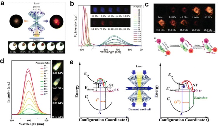 | ||
| Fig. 13 (a) Schematic diagram of 1D EAPbI3 luminescence intensity increasing with pressure. Reproduced with permission.24 2020 American Chemical Society. (b) PL spectra of (PEA)2PbBr4 as a function of pressure and PL micrographs upon compression. Reproduced with permission.26 2019 Wiley-VCH Verlag GmbH. (c) The photomicrograph shows the enhanced emission of (BA)4AgBiBr8 with increasing pressure. Reprinted with permission.27 Copyright 2019 Wiley-VCH. (d) Pressure-dependence of the PL spectra of C4N2H14SnBr4. (e) Schematic diagram of the pressure-induced emission mechanism of self-trapped exciton. Reproduced with permission.25 Copyright 2019 American Chemical Society. | ||
3.5. Doping metal ions to enhance luminescence
Doping metals would be an effective strategy to tune the luminescence performance and improve the PLQE of LDMHs.98 For example, extensive research on Mn2+ doping has been carried out due to exciton energy transition between from the FEs to the Mn2+ d-states and the internal transition of Mn2+ ions from 4T1 to 6A1; thus, a low-energy emission peak at about 600 nm was produced.99 Cheng et al. grew a centimeter-size 2D layered (CH3NH3)2MnCl4 single crystal (Fig. 14(a)) and illustrated the temperature-dependent PL spectra (Fig. 14(b)).100 Obviously, the PL intensity of (CH3NH3)2MnCl4 increases with decreasing temperature. The efficient emission was obtained thanks to the electronic transition (t2g)3(eg)2–(t2g)4(eg)1 of the Mn2+ ions (Fig. 14(c)).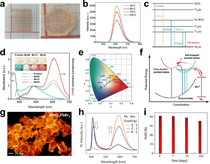 | ||
| Fig. 14 (a) Photographs of layered (CH3NH3)2MnCl4 single crystals; (b) temperature-dependent luminescence spectra of (CH3NH3)2MnCl4 single crystals; (c) schematic diagram showing the energy absorption and emission processes of (CH3NH3)2MnCl4; reproduced with permission.100 Copyright 2019 The Royal Society of Chemistry. (d) Absorption and emission spectra of the pristine and Mn-doped 1D C4N2H14PbBr4, the inset shows the images of the pristine and Mn-doped C4N2H14PbBr4 under ambient light (top) and UV light (365 nm, bottom); (e) CIE coordinates of the emissions of the pristine and Mn-doped C4N2H14PbBr4 upon UV excitation; (f) proposed energy diagram and excited state dynamics of Mn-doped 1D C4N2H14PbBr4; reproduced with permission.28 Copyright 2017 American Chemical Society. (g) Optical microscopic images of Mn-doped L2PbBr4 microcrystals under UV irradiation; (h) PL spectra of Mn-doped L2PbBr4; (i) PLQE stability of Mn-doped L2PbBr4 microcrystals; reproduced with permission.103 Copyright 2019 American Chemical Society. | ||
Zhou et al.28 reported an Mn2+-doped 1D C4N2H14PbBr4 with bright white emission, and the PL spectra and the images (inset) of the series of Mn-doped C4N2H14PbBr4 upon UV excitation are shown in Fig. 14(d). Dual emission at ∼390 and ∼485 nm recorded for pristine C4N2H14PbBr4 originates from FEs and STEs states. Eventually, efficient white emissions were obtained in Mn2+-doped 1D C4N2H14PbBr4 by combining the broadband blue emission of STEs and red emission originating from the d–d transition of Mn2+.101 The CIE coordinates of the Mn2+-doped C4N2H14PbBr4 was displayed in Fig. 14(e), and the CRI and PLQE of Mn2+-doped C4N2H14PbBr4 were increased to 87 and 28%, respectively. In the Mn2+-doped C4N2H14PbBr4, the blue emission at ∼485 nm remains relatively unchanged, but the near-UV emission is obviously quenched at 390 nm and an additional broadband emission appeared at 605 nm due to ligand field transition (4T1 to 6A1) of Mn2+ (Fig. 14(f)).102 Dutta et al. synthesized a layered Mn2+-doped L2PbX4 (X = Cl, Br, I) single crystal using a solution-phase colloidal approach (Fig. 14(g)).103 Mn2+-doped L2PbX4 presents additional dopant emission at about 600 nm, when the intrinsic emission located at 420 nm (Fig. 14(h)). Moreover, doping Mn2+ facilitates exciton energy transition and achieves satisfactory PLQE of ∼61%. Fig. 14(i) indicates the stability in retaining intense emission of Mn2+-doped L2PbX4 microcrystals under ambient conditions.
In addition to doping Mn2+, other doping metals elements in LDMHs have been investigated to improve the luminescence efficiency and avoid the proportion of toxic lead, such as Sn3+,31,104 Sb2+,98a,98b Bi3+,105 Fe3+,106 In+,107 Na+,108 Ag+,109 and multicomponent metal.110Fig. 15(a) and (b) show the fabricated image and crystal structure of 0D (C8NH12)4Bi0.57Sb0.43Br7·H2O single crystal by Zhang et al.,30 and the ratio of Pb and Sb (0.59![[thin space (1/6-em)]](https://www.rsc.org/images/entities/char_2009.gif) :
:![[thin space (1/6-em)]](https://www.rsc.org/images/entities/char_2009.gif) 0.41) in single crystals was estimated by energy dispersive spectroscopy (EDS), as depicted in Fig. 15(e). Moreover, compared to (C8NH12)4BiBr7·H2O and the reported 0D Sn-based perovskites,104 different PL properties were reported in (C8NH12)4Bi0.57Sb0.43Br7·H2O. The super broadband emission with 400 to 850 nm was exhibited in Fig. 15(c), and the PLQE increases from 0.7% to 4.5%. The TA spectra confirmed the STEs (Fig. 15(d)). As shown in Fig. 15(f), the mechanism of super broadband emission was attributed to the synergistic effect of FEs and STEs in the [BiBr6]3− and [SbBr6]3− species. The FEs are captured by the intrinsic STEs state, followed by energy transfer to the newly generated STEs state caused by the addition of the [SbBr6]3− species.111 Finally, the PLQE of super broadband emission was significantly enhanced due to the singlet and triplet STEs.112 Wei et al. reported a series of 0D In–Sb doped BAPPIn2−2xSb2xCl10 (BAPP = C10H28N4, x = 0–1) perovskite single crystals with adjustable emission.107 As shown in Fig. 15(g), a series of BAPPIn2−2xSb2xCl10 single crystals show different colored emission under irradiation condition of UV light (λex = 365 nm) with different doped contents of Sb. Interestingly, with the addition of Sb, there are obvious blue and yellow double emission bands (∼440 and ∼560 nm) in the PL spectrum. Moreover, a series of BAPPIn2−2xSb2xCl10 materials were used in the field of anti-counterfeiting due to their excellent properties, such as afterglow emission, as well as high spatial and temporal resolution. Fig. 15(h) displays a 2020-shaped module-filled BAPPIn1.996Sb0.004Cl10 powders, which displays a misleading profile with 8888-shaped under visible light and changes to a yellow-white emission with 2020-shaped under condition of 254 and 365 nm, respectively. The organic emission of BAPPSb2Cl10 was almost quenched, which may be due to the energy transfer of the organic cation widely present in the doped system to the Sb3+ emission center. In this case, the two launch centers operate independently, providing a perfect complement of colors, namely, blue and yellow emission, which eventually appear as a bright white emission (Fig. 15(i)). The WLED device and CIE coordinates of the emissions are depicted in Fig. 15(j), and distinguishable fluorescence colors of the as-fabricated flexible BAPPIn1.996Sb0.004Cl10-PDMS (polydimethylsiloxane) are seen at 365 and 254 nm UV light (Fig. 15(k)).
0.41) in single crystals was estimated by energy dispersive spectroscopy (EDS), as depicted in Fig. 15(e). Moreover, compared to (C8NH12)4BiBr7·H2O and the reported 0D Sn-based perovskites,104 different PL properties were reported in (C8NH12)4Bi0.57Sb0.43Br7·H2O. The super broadband emission with 400 to 850 nm was exhibited in Fig. 15(c), and the PLQE increases from 0.7% to 4.5%. The TA spectra confirmed the STEs (Fig. 15(d)). As shown in Fig. 15(f), the mechanism of super broadband emission was attributed to the synergistic effect of FEs and STEs in the [BiBr6]3− and [SbBr6]3− species. The FEs are captured by the intrinsic STEs state, followed by energy transfer to the newly generated STEs state caused by the addition of the [SbBr6]3− species.111 Finally, the PLQE of super broadband emission was significantly enhanced due to the singlet and triplet STEs.112 Wei et al. reported a series of 0D In–Sb doped BAPPIn2−2xSb2xCl10 (BAPP = C10H28N4, x = 0–1) perovskite single crystals with adjustable emission.107 As shown in Fig. 15(g), a series of BAPPIn2−2xSb2xCl10 single crystals show different colored emission under irradiation condition of UV light (λex = 365 nm) with different doped contents of Sb. Interestingly, with the addition of Sb, there are obvious blue and yellow double emission bands (∼440 and ∼560 nm) in the PL spectrum. Moreover, a series of BAPPIn2−2xSb2xCl10 materials were used in the field of anti-counterfeiting due to their excellent properties, such as afterglow emission, as well as high spatial and temporal resolution. Fig. 15(h) displays a 2020-shaped module-filled BAPPIn1.996Sb0.004Cl10 powders, which displays a misleading profile with 8888-shaped under visible light and changes to a yellow-white emission with 2020-shaped under condition of 254 and 365 nm, respectively. The organic emission of BAPPSb2Cl10 was almost quenched, which may be due to the energy transfer of the organic cation widely present in the doped system to the Sb3+ emission center. In this case, the two launch centers operate independently, providing a perfect complement of colors, namely, blue and yellow emission, which eventually appear as a bright white emission (Fig. 15(i)). The WLED device and CIE coordinates of the emissions are depicted in Fig. 15(j), and distinguishable fluorescence colors of the as-fabricated flexible BAPPIn1.996Sb0.004Cl10-PDMS (polydimethylsiloxane) are seen at 365 and 254 nm UV light (Fig. 15(k)).
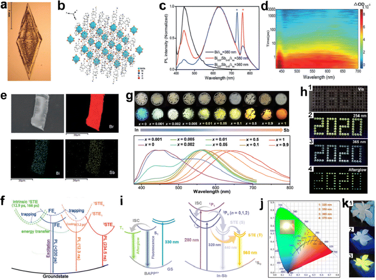 | ||
| Fig. 15 (a) and (b) Image and structure diagram of the (C8NH12)4Bi0.57Sb0.43Br7·H2O single crystal; (c) room temperature PL spectra of (C8NH12)4BiBr7·H2O and (C8NH12)4Bi0.57Sb0.43Br7·H2O; (d) contour plot of the fs TA spectrum upon photoexcitation at 320 nm, (e) EDS elemental mapping of Br, Bi, and Sb elements; (f) schematic energy level diagram of (C8NH12)4Bi0.57Sb0.43Br7·H2O single crystal; reproduced with permission.30 Copyright 2019 Wiley-VCH. (g) Images and PL spectra under visible and UV light of a batch of BAPPIn2−2xSb2xCl10; (h) photos of patterned single BAPPIn1.996Sb0.004Cl10 crystals under the excitation of (1) visible light, (2) 254 nm UV light, (3) 365 nm UV light on, and (4) 365 nm UV light off (afterglow); (i) schematic illustration of the photophysical processes in BAPPIn2−2xSb2xCl10; (j) excitation wavelength-dependent CIE coordinate diagram of BAPPIn1.996Sb0.004Cl10 (inset is the image of working WLED); (k) images of leaf-like shape BAPPIn1.996Sb0.004Cl10-PDMS complex under (1) visible light, (2) 365 nm UV light, and (3) 254 nm UV light, respectively; reproduced with permission.107 Copyright 2021 American Association for the Advancement of Science. | ||
Yu et al.31 reported Sn-doped 2D PEA2PbI4 (PEA = phenylethylammonium) crystal (Fig. 16(a)), which produces broadband emission with red-to-near-infrared thanks to the stronger exciton–phonon coupling, and the PLQE is significantly increased from 0.7% to 6.0%. PEA2PbI4 and doped 0.36%-Sn PEA2PbI4 generate green emission at 525 nm and bright broadband emission with red-to-near-infrared at the center of 710 nm (Fig. 16(b)). The emissions of PEA2PbI4 and Sn-doped PEA2PbI4 depend on exciton dynamics confined to the inorganic layer (Fig. 16(c)) and the relaxation channels of carriers in the excited perovskite (Fig. 16(d)). Zhang et al. synthesized two 2D (PEA)4NaInCl8:Sb and (PEA)2CsNaInCl7:Sb single crystals by doping Sb.108 The STEs captured in the introduced [SbCl6]3− octahedron produced bright broadband emission with PLQE of 48.7%. The main dynamic process of initial and Sb-doped (PEA)4NaInCl8 is depicted in Fig. 16(e); the doped [SbCl6]3− octahedron offers a new exciton capturing center and forms a Jahn–Teller-like distortion under the condition of excited state. The PL intensity of (PEA)4NaInCl8:Sb increased first and then decreased with the increase in the Sb content, and the optimal doping ratio is 2.13% (Fig. 16(f)).
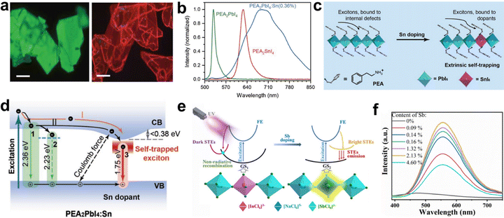 | ||
| Fig. 16 (a) Fluorescence microscopy images of PEA2PbI4 and PEA2PbI4:Sn(0.36%) crystals. Scale bar: 100 μm; (b) microscopic PL spectra under λex = 470 nm; (c) schematic illustration of exciton trapping in pristine and Sn-doped 2D PEA2PbI4; (d) schematic illustration of radiative channels in Sn-doped PEA2PbI4. Arabic numerals 1, 2, and 3 represent the luminescence from free, bound excitons of pristine perovskite, and Sn-triggered STEs of Sn-doped perovskite, respectively; reproduced with permission.31 Copyright 2018 Wiley-VCH. (e) Schematic energy level diagrams of (PEA)4NaInCl8 and (PEA)4NaInCl8:Sb; (f) PL spectra of (PEA)4NaInCl8:Sb with different Sb contents (Sb/In); reproduced with permission.108 Copyright 2021 Wiley-VCH. | ||
In summary, both the internal components and external factors can modulate the STE emission of LDMHs. For internal components, choosing the large organic cations with polyamine groups or long chain amine can distort the inorganic skeleton, thus favoring exciton self-trapping. Passing from I, Br, to Cl, it tends to form STE broadband emission. In addition, the LDMHs with strong electron–phonon coupling (large S) generally produce STE emission. For the external factors, STE emission can be induced by proper pressure, and decreasing the temperature can inhibit exciton detrapping and enhance STE emission. Furthermore, doping metal ions is also an effective way to modulate the STE emission and improve the PLQE of LDMHs, such as doping Mn2+ and Sn2+.
4. Prospects and outlook
(1) Solid-state lighting is emerging in the automotive, architectural, and general lighting markets over the last decade. Despite significant progress in white light-emitting diodes (WLED), there are still many problems and challenges that limit its development, for example, single color rendering is usually poor due to the discontinuity of the emission spectrum. On the other hand, mixing phosphors will decrease in efficiency due to the self-absorption effect. At the same time, the luminous color of phosphors varies with time due to different attenuation degrees. To solve these problems, an ideal solution is to develop a single component of broadband spectrum white phosphor powder excited by ultraviolet light. At present, this material is relatively rare. Most of them are inorganic materials doped with rare earth elements. The luminescence efficiency of these inorganic phosphors is generally low, and the manufacturing process is complex and the manufacturing cost is higher. For these reasons, it is very important to develop new types of white phosphor. The organic–inorganic hybrid LDMHs is a very promising illuminating material for WLED.(2) Compared with 3D perovskites, the selection of organic cations for LDMHs is more abundant. We can not only regulate the structural dimension by selecting organic cations in large size but also rationally design organic cations to achieve the regulation of photoelectric properties. LDMHs exhibit excellent luminescence due to their quantum confined effect and large exciton binding energies. Also, by the rational design of organic cations, their emission type, fluorescence quantum efficiency, and so on can be regulated.
(3) In addition, LDMHs are not limited to the application on LEDs. Their photoelectric response characteristics make them promising materials for photodetectors, lasers, biosensors, and ferroelectric response devices. Multifunctional LDMHs with abundant dimensions and structures are looking forward to the potential applications.
Overcoming
(1) However, the origin of the broadband emission in LDMHs is still hotly debated. Different mechanisms have recently been proposed to explain the origin of such emission. These contradicting explanations reported in the literature motivated us to decipher the source of broadband emission. Figuring out the luminescence mechanism will enable the development of synthesis strategies that fully control the broadband luminescence and defect properties.(2) LDMHs has been widely used in LED devices due to its high exciton binding energy, but there is still a long way to go in the development of phosphorescent materials and the technology of large-area LED devices. At present, LDMHs for red/green LED devices have been investigated by many researches, but there are still few reports on new material and luminescence mechanism in the development of blue LED. Moreover, device fabrication processes are still immature, including large-area LED and heterostructure devices.
(3) Although the stability of organic–inorganic hybrid perovskites has been greatly improved, the potential toxicity problem of Pb2+ has not been solved. Decrease environmental pollution is a key issue. At present, some people have tried to use other metal elements to replace or partially replace Pb to prepare lead-free or lead-less LDMHs. At present, it has been reported that Cu2+, Mn2+, Zn2+, and other metal LDMHs show excellent luminescence characteristics; however, more mixing or doping metal LDMHs remain largely unexplored.
Author contributions
Y. Han and X. Cheng contributed equally to this work. All the authors contibuted to the discussion on the content, writing and editing for this menuscript prior to submission.Conflicts of interest
The authors declare no competing interests.Acknowledgements
This work was supported by funding from the National Natural Science Foundation (21703008 and 22075022) and the “Cultivate Creative Talents Project” of Beijing Institute of Technology (BIT).References
- (a) H. Lu, Y. Liu, P. Ahlawat, A. Mishra, W. R. Tress, F. T. Eickemeyer, Y. Yang, F. Fu, Z. Wang and C. E. Avalos, Science, 2020, 370 Search PubMed; (b) X.-K. Liu, W. Xu, S. Bai, Y. Jin, J. Wang, R. H. Friend and F. Gao, Nat. Mater., 2020, 1–12 Search PubMed.
- (a) H. Lin, C. Zhou, Y. Tian, T. Siegrist and B. Ma, ACS Energy Lett., 2018, 3, 54–62 CrossRef CAS; (b) T. Zhu and X. Gong, InfoMat, 2021, 3, 1039–1069 CrossRef CAS.
- Q. Yao, J. Zhang, K. Wang, L. Jing, X. Cheng, C. Shang, J. Ding, W. Zhang, H. Sun and T. Zhou, J. Mater. Chem. C, 2021, 9, 7374–7383 RSC.
- H. Lin, C. Zhou, Y. Tian, T. Siegrist and B. Ma, ACS Energy Lett., 2017, 3, 54–62 CrossRef.
- H.-P. Wang, S. Li, X. Liu, Z. Shi, X. Fang and J.-H. He, Adv. Mater., 2021, 33, 2003309 CrossRef CAS PubMed.
- D. Yu, P. Wang, F. Cao, Y. Gu, J. Liu, Z. Han, B. Huang, Y. Zou, X. Xu and H. Zeng, Nat. Commun., 2020, 11, 3395 CrossRef CAS PubMed.
- K. Park, J. W. Lee, J. D. Kim, N. S. Han, D. M. Jang, S. Jeong, J. Park and J. K. Song, J. Phys. Chem. Lett., 2016, 7, 3703–3710 CrossRef CAS PubMed.
- G. Zhou, M. Li, J. Zhao, M. S. Molokeev and Z. Xia, Adv. Opt. Mater., 2019, 7, 1901335 CrossRef CAS.
- J. Zhang, X. Yang, H. Deng, K. Qiao, U. Farooq, M. Ishaq, F. Yi, H. Liu, J. Tang and H. Song, Nano-Micro Lett., 2017, 9, 36 CrossRef PubMed.
- (a) N. Kawano, M. Koshimizu, G. Okada, Y. Fujimoto, N. Kawaguchi, T. Yanagida and K. Asai, Sci. Rep., 2017, 7, 1–8 CrossRef CAS PubMed; (b) L. Zhou, J. F. Liao, Z. G. Huang, J. H. Wei, X. D. Wang, W. G. Li, H. Y. Chen, D. B. Kuang and C. Y. Su, Angew. Chem., Int. Ed., 2019, 58, 5277–5281 CrossRef CAS PubMed; (c) B.-B. Cui, N. Yang, C. Shi, S. Yang, J.-Y. Shao, Y. Han, L. Zhang, Q. Zhang, Y.-W. Zhong and Q. Chen, J. Mater. Chem. A, 2018, 6, 10057–10063 RSC; (d) Z. Yuan, C. Zhou, Y. Tian, Y. Shu, J. Messier, J. C. Wang, L. J. van de Burgt, K. Kountouriotis, Y. Xin and E. Holt, Nat. Commun., 2017, 8, 14051 CrossRef CAS PubMed.
- L. Mao, C. C. Stoumpos and M. G. Kanatzidis, J. Am. Chem. Soc., 2019, 141, 1171–1190 CrossRef CAS PubMed.
- (a) L. Mao, Y. Wu, C. C. Stoumpos, M. R. Wasielewski and M. G. Kanatzidis, J. Am. Chem. Soc., 2017, 139, 5210–5215 CrossRef CAS PubMed; (b) E. R. Dohner, E. T. Hoke and H. I. Karunadasa, J. Am. Chem. Soc., 2014, 136, 1718–1721 CrossRef CAS PubMed; (c) E. R. Dohner, A. Jaffe, L. R. Bradshaw and H. I. Karunadasa, J. Am. Chem. Soc., 2014, 136, 13154–13157 CrossRef CAS PubMed.
- A. A. Zhumekenov, M. I. Saidaminov, O. F. Mohammed and O. M. Bakr, Joule, 2021, 5, 2027 CrossRef CAS.
- C. M. Iaru, J. J. Geuchies, P. M. Koenraad, D. L. Vanmaekelbergh and A. Y. Silov, ACS Nano, 2017, 11, 11024–11030 CrossRef CAS PubMed.
- D. Y. Park, S. J. An, C. Lee, D. A. Nguyen, K. N. Lee and M. S. Jeong, J. Phys. Chem. Lett., 2019, 10, 7942–7948 CrossRef CAS PubMed.
- Q. Zhang, Y. Ji, Z. Chen, D. Vella, X. Wang, Q. H. Xu, Y. Li and G. Eda, J. Phys. Chem. Lett., 2019, 10, 2869–2873 CrossRef CAS PubMed.
- (a) M. D. Smith, A. Jaffe, E. R. Dohner, A. M. Lindenberg and H. I. Karunadasa, Chem. Sci., 2017, 8, 4497–4504 RSC; (b) B. Febriansyah, T. Borzda, D. Cortecchia, S. Neutzner, G. Folpini, T. M. Koh, Y. Li, N. Mathews, A. Petrozza and J. England, Angew. Chem., Int. Ed., 2020, 59, 10791 CrossRef CAS PubMed.
- M. D. Smith, A. Jaffe, E. R. Dohner, A. M. Lindenberg and H. I. Karunadasa, Chem. Sci., 2017, 8, 4497–4504 RSC.
- L. Mao, Y. Wu, C. C. Stoumpos, M. R. Wasielewski and M. G. Kanatzidis, J. Am. Chem. Soc., 2017, 139, 5210–5215 CrossRef CAS PubMed.
- C. Li, J. Yang, F. Su, J. Tan, Y. Luo and S. Ye, Nat. Commun., 2020, 11, 1–8 CrossRef PubMed.
- (a) K. Wang, Y. Yuan, S. Du, Q. Yao, J. Zhang, C. Shang, C. Li, H. Sun, W. Zhang, J. Ding and T. Zhou, J. Phys. Chem. C, 2021, 125, 15223–15232 CrossRef CAS; (b) M. D. Smith, B. A. Connor and H. I. Karunadasa, Chem. Rev., 2019, 119, 3104–3139 CrossRef CAS PubMed.
- Y. Gao, E. Shi, S. Deng, S. B. Shiring, J. M. Snaider, C. Liang, B. Yuan, R. Song, S. M. Janke and A. Liebman-Peláez, Nat. Chem., 2019, 11, 1151–1157 CrossRef CAS PubMed.
- X. Gong, O. Voznyy, A. Jain, W. Liu, R. Sabatini, Z. Piontkowski, G. Walters, G. Bappi, S. Nokhrin and O. Bushuyev, Nat. Mater., 2018, 17, 550–556 CrossRef CAS PubMed.
- Y. Liang, Y. Zang, X. Huang, C. Tian, X. Wang and T. Cui, J. Phys. Chem. C, 2020, 124, 8984–8991 CrossRef CAS.
- Y. Shi, Z. Ma, D. Zhao, Y. Chen and Y. Cao, J. Am. Chem. Soc., 2019, 141(16), 6504–6508 CrossRef CAS PubMed.
- L. Zhang, L. Wu, K. Wang and B. Zou, Adv. Sci., 2019, 6, 1801628 CrossRef PubMed.
- Y. Fang, L. Zhang, L. Wu, J. Yan and B. Zou, Angew. Chem., Int. Ed., 2019, 58, 15249 CrossRef CAS PubMed.
- C. Zhou, Y. Tian, O. Khabou, M. Worku, Y. Zhou, J. Hurley, H. Lin and B. Ma, ACS Appl. Mater. Interfaces, 2017, 9, 40446–40451 CrossRef CAS PubMed.
- Z. Li, Y. Li, P. Liang, T. Zhou, L. Wang and R.-J. Xie, Chem. Mater., 2019, 31, 9363–9371 CrossRef CAS.
- R. Zhang, X. Mao, Y. Yang, S. Yang, W. Zhao, T. Wumaier, D. Wei, W. Deng and K. Han, Angew. Chem., Int. Ed., 2019, 58, 2725–2729 CrossRef CAS PubMed.
- J. Yu, J. Kong, W. Hao, X. Guo, H. He, W. R. Leow, Z. Liu, P. Cai, G. Qian, S. Li, X. Chen and X. Chen, Adv. Mater., 2019, 31, e1806385 Search PubMed.
- (a) C. Zhou, H. Lin, Y. Tian, Z. Yuan, R. Clark, B. Chen, J. Neu, T. Besara, T. Siegrist, E. Lambers, P. Djurovich and B. Ma, Chem. Sci., 2018, 9, 586 RSC; (b) B.-B. Cui, Y. Han, B. Huang, Y. Zhao, X. Wu, L. Liu, G. Cao, Q. Du, N. Liu and W. Zou, Nat. Commun., 2019, 10, 1–8 CAS.
- Z. Wu, C. Ji, Z. Sun, S. Wang, S. Zhao, W. Zhang, L. Li and J. Luo, J. Mater. Chem. C, 2018, 6, 1171–1175 RSC.
- L. Mao, Y. Wu, C. C. Stoumpos, B. Traore, C. Katan, J. Even, M. R. Wasielewski and M. G. Kanatzidis, J. Am. Chem. Soc., 2017, 139, 11956–11963 CrossRef CAS PubMed.
- (a) W. P. Wong, J. Yin, B. Chaudhary, X. Y. Chin, D. Cortecchia, S.-Z. A. Lo, A. C. Grimsdale, O. F. Mohammed, G. Lanzani and C. Soci, ACS Mater. Lett., 2019, 2, 20–27 CrossRef; (b) D. Ghosh, E. Welch, A. J. Neukirch, A. Zakhidov and S. Tretiak, J. Phys. Chem. Lett., 2020, 11, 3271–3286 CrossRef CAS PubMed.
- M. D. Smith and H. I. Karunadasa, Acc. Chem. Res., 2018, 51(3), 619–627 CrossRef CAS PubMed.
- C. Zhou, H. Lin, H. Shi, Y. Tian and B. Ma, Angew. Chem., Int. Ed., 2017, 130 Search PubMed.
- J. Yin, H. Li, D. Cortecchia, C. Soci and J.-L. Brédas, ACS Energy Lett., 2017, 2, 417–423 CrossRef CAS.
- (a) P. Cai, Y. Huang and H. J. Seo, J. Phys. Chem. Lett., 2019, 10, 4095–4102 CrossRef CAS PubMed; (b) A. Biswas, R. Bakthavatsalam, S. R. Shaikh, A. Shinde, A. Lohar, S. Jena, R. G. Gonnade and J. Kundu, Chem. Mater., 2019, 31, 2253–2257 CrossRef CAS.
- D. Cortecchia, S. Neutzner, A. R. Srimath Kandada, E. Mosconi, D. Meggiolaro, F. De Angelis, C. Soci and A. Petrozza, J. Am. Chem. Soc., 2017, 139, 39–42 CrossRef CAS PubMed.
- (a) L. Zhou, J. F. Liao, Z. G. Huang, J. H. Wei, X. D. Wang, H. Y. Chen and D. B. Kuang, Angew. Chem., Int. Ed., 2019, 131, 15581–15586 CrossRef; (b) D. Han, H. Shi, W. Ming, C. Zhou, B. Ma, B. Saparov, Y.-Z. Ma, S. Chen and M.-H. Du, J. Mater. Chem. C, 2018, 6, 6398–6405 RSC.
- X. Wang, W. Meng, W. Liao, J. Wang, R.-G. Xiong and Y. Yan, J. Phys. Chem. Lett., 2019, 10, 501–506 CrossRef CAS PubMed.
- S. Kahmann, E. K. Tekelenburg, H. Duim, M. E. Kamminga and M. A. Loi, Nat. Commun., 2020, 11, 1–8 CrossRef PubMed.
- J. Yin, R. Naphade, L. Gutiérrez Arzaluz, J.-L. Bredas, O. M. Bakr and O. F. Mohammed, ACS Energy Lett., 2020, 5(7), 2149–2155 CrossRef CAS.
- A. Wang, Y. Guo, Z. Zhou, X. Niu, Y. Wang, F. Muhammad, H. Li, T. Zhang, J. Wang, S. Nie and Z. Deng, Chem. Sci., 2019, 10, 4573 RSC.
- B. Dhanabalan, R. D. Pothuraju, S. Marras, L. Pasquale, L. Manna, R. Krahne and M. P. Arciniegas, Adv. Photon. Res., 2021, 2, 2100005 CrossRef.
- (a) Z. Yuan, C. Zhou, Y. Tian, Y. Shu, J. Messier, J. C. Wang, L. J. Van De Burgt, K. Kountouriotis, Y. Xin and E. Holt, Nat. Commun., 2017, 8, 14051 CrossRef CAS PubMed; (b) R. Gautier, F. Massuyeau, G. Galnon and M. Paris, Adv. Mater., 2019, 31, 1807383 CrossRef.
- C. Zhou, H. Lin, Y. Tian, Z. Yuan, R. Clark, B. Chen, L. J. van de Burgt, J. C. Wang, Y. Zhou and K. Hanson, Chem. Sci., 2018, 9, 586–593 RSC.
- S. Wang, Y. Yao, J. Kong, S. Zhao, Z. Sun, Z. Wu, L. Li and J. Luo, Chem. Commun., 2018, 54, 4053–4056 RSC.
- (a) I. Neogi, A. Bruno, D. Bahulayan, T. W. Goh, B. Ghosh, R. Ganguly, D. Cortecchia, T. C. Sum, C. Soci and N. Mathews, ChemSusChem, 2017, 10, 3765–3772 CrossRef CAS PubMed; (b) H. Hu, S. A. Morris, X. Qiao, D. Zhao, T. Salim, B. Chen, E. E. Chia and Y. M. Lam, J. Mater. Chem. C, 2018, 6, 10301–10307 RSC; (c) M. D. Smith, A. Jaffe, E. R. Dohner, A. M. Lindenberg and H. I. Karunadasa, Chem. Sci., 2017, 8, 4497–4504 RSC.
- B. Febriansyah, T. Borzda, D. Cortecchia, S. Neutzner, G. Folpini, T. M. Koh, Y. Li, N. Mathews, A. Petrozza and J. England, Angew. Chem., Int. Ed., 2020, 59, 10791–10796 CrossRef CAS PubMed.
- S. Wang, Y. Yao, Z. Wu, Y. Peng, L. Li and J. Luo, J. Mater. Chem. C, 2018, 6, 12267–12272 RSC.
- L. Mao, Y. Wu, C. C. Stoumpos, B. Traore, C. Katan, J. Even, M. R. Wasielewski and M. G. Kanatzidis, J. Am. Chem. Soc., 2017, 139, 5210–5215 CrossRef CAS PubMed.
- A. Yangui, S. Pillet, A. Lusson, E. E. Bendeif, S. Triki, Y. Abid and K. Boukheddaden, J. Alloys Compd., 2017, 699, 1122–1133 CrossRef CAS.
- D. Cortecchia, J. Yin, A. Petrozza and C. Soci, J. Mater. Chem. C, 2019, 7, 4956–4969 RSC.
- Y. Y. Pan, Y. H. Su, C. H. Hsu, L. W. Huang and C. C. Kaun, Comput. Mater. Sci., 2016, 117, 573–578 CrossRef CAS.
- A. Lemmerer and D. G. Billing, CrystEngComm, 2012, 14, 1954–1966 RSC.
- Y. Han, Y. Li, Y. Wang, G. Cao, S. Yue, L. Zhang, B. B. Cui and Q. Chen, Adv. Opt. Mater., 2020, 8, 1902051 CrossRef CAS.
- M. E. Kamminga, H. H. Fang, M. R. Filip, F. Giustino, J. Baas, G. R. Blake, M. A. Loi and T. T. M. Palstra, Chem. Mater., 2016, 28(13), 4554–4562 CrossRef CAS.
- L. L. Mao, P. J. Guo, M. Kepenekian, I. Hadar, C. Katan., J. Even, R. D. Schaller, C. C. Stoumpos and M. K. Kanatzidis, J. Am. Chem. Soc., 2018, 140(40), 13078–13088 CrossRef CAS PubMed.
- M. Zhang, L. Zhao, J. Xie, Q. Zhang, X. Wang, N. Yaqoob, Z. Yin, P. Kaghazchi, H. Li and C. Zhang, Nat. Commun., 2021, 12, 1–7 CrossRef PubMed.
- S. Krishnamurthy, R. Naphade, W. J. Mir, S. Gosavi, S. Chakraborty, R. Vaidhyanathan and S. Ogale, Adv. Opt. Mater., 2018, 6, 1800751 CrossRef.
- A. Yangui, D. Garrot, J.-S. Lauret, A. Lusson, G. Bouchez, E. Deleporte, S. Pillet, E.-E. Bendeif, M. Castro and S. Triki, J. Phys. Chem. C, 2015, 119, 23638–23647 CrossRef CAS.
- T. Dammak and Y. Abid, Opt. Mater., 2017, 66, 302–307 CrossRef CAS.
- Y. Peng, Y. Yao, L. Li, Z. Wu, S. Wang and J. Luo, J. Mater. Chem. C, 2018, 6, 6033–6037 RSC.
- G.-E. Wang, G. Xu, M.-S. Wang, L.-Z. Cai, W.-H. Li and G.-C. Guo, Chem. Sci., 2015, 6, 7222–7226 RSC.
- (a) B. Dhanabalan, Y. C. Leng, G. Biffi, M. L. Lin, P. H. Tan, I. Infante, L. Manna, M. P. Arciniegas and R. Krahne, ACS Nano, 2020, 14, 4689–4697 CrossRef CAS PubMed; (b) D. B. Straus, S. Hurtado Parra, N. Iotov, J. Gebhardt, A. M. Rappe, J. E. Subotnik, J. M. Kikkawa and C. R. Kagan, J. Am. Chem. Soc., 2016, 138, 13798–13801 CrossRef CAS PubMed; (c) F. Thouin, D. A. Valverde-Chavez, C. Quarti, D. Cortecchia, I. Bargigia, D. Beljonne, A. Petrozza, C. Silva and A. R. Srimath Kandada, Nat. Mater., 2019, 18, 349–356 CrossRef CAS PubMed.
- (a) C. M. Iaru, J. J. Geuchies, P. M. Koenraad, D. Vanmaekelbergh and A. Y. Silov, ACS Nano, 2017, 11, 11024–11030 CrossRef CAS PubMed; (b) A. D. Wright, C. Verdi, R. L. Milot, G. E. Eperon, M. A. Perez-Osorio, H. J. Snaith, F. Giustino, M. B. Johnston and L. M. Herz, Nat. Commun., 2016, 7 Search PubMed.
- R. F. Moral, J. C. Germino, L. G. Bonato, D. B. Almeida, E. M. Therézio, T. D. Atvars, S. D. Stranks, R. A. Nome and A. F. Nogueira, Adv. Opt. Mater., 2020, 8, 2001431 CrossRef CAS.
- (a) N. S. Makarov, S. Guo, O. Isaienko, W. Liu, I. Robel and V. I. Klimov, Nano Lett., 2016, 16, 2349–2362 CrossRef CAS PubMed; (b) J. Fu, Q. Xu, G. Han, B. Wu, C. H. A. Huan, M. L. Leek and T. C. Sum, Nat. Commun., 2017, 8, 1300 CrossRef PubMed; (c) M. B. Price, J. Butkus, T. C. Jellicoe, A. Sadhanala, A. Briane, J. E. Halpert, K. Broch, J. M. Hodgkiss, R. H. Friend and F. Deschler, Nat. Commun., 2015, 6, 8420 CrossRef CAS PubMed; (d) M. E. Madjet, G. R. Berdiyorov, F. El-Mellouhi, F. H. Alharbi, A. V. Akimov and S. Kais, J. Phys. Chem. Lett., 2017, 8, 4439–4445 CrossRef CAS PubMed.
- L. Ni, U. Huynh, A. Cheminal, T. H. Thomas, R. Shivanna, T. F. Hinrichsen, S. Ahmad, A. Sadhanala and A. Rao, ACS Nano, 2017, 11, 10834 CrossRef CAS PubMed.
- Q. Du, C. Zhu, Z. Yin, G. Na, C. Cheng, Y. Han, N. Liu, X. Niu, H. Zhou and H. Chen, ACS Nano, 2020, 14, 5806–5817 CrossRef CAS PubMed.
- S.-F. Zhang, X.-K. Chen, A.-M. Ren, H. Li and J.-L. Bredas, ACS Energy Lett., 2018, 4, 17–25 CrossRef.
- J. Yin, P. Maity, R. Naphade, B. Cheng, J. H. He, O. M. Bakr, J. L. Bredas and O. F. Mohammed, ACS Nano, 2019, 13, 12621–12629 CrossRef CAS PubMed.
- Y. Han, J. Yin, G. Cao, Z. Yin, Y. Dong, R. Chen, Y. Zhang, N. Li, S. Jin, O. F. Mohammed, B.-B. Cui and Q. Chen, ACS Energy Lett., 2021, 453 Search PubMed.
- J. Luo, X. Wang, S. Li, J. Liu, Y. Guo, G. Niu, L. Yao, Y. Fu, L. Gao and Q. Dong, Nature, 2018, 563, 541 CrossRef CAS PubMed.
- R. Zeng, L. Zhang, Y. Xue, B. Ke, Z. Zhao, D. Huang, Q. Wei, W. Zhou and B. Zou, J. Phys. Chem. Lett., 2020, 11, 2053 CrossRef CAS PubMed.
- K. M. McCall, C. C. Stoumpos, S. S. Kostina, M. G. Kanatzidis and B. W. Wessels, Chem. Mater., 2017, 29, 4129 CrossRef CAS.
- H. Siddique, Z. Xu, X. Li, S. Saeed, W. Liang, X. Wang, C. Gao, R. Dai, Z. Wang and Z. Zhang, J. Phys. Chem. Lett., 2020, 11, 9572 CrossRef CAS PubMed.
- S. Zelewski, J. Urban, A. Surrente, D. Maude, A. Kuc, L. Schade, R. Johnson, M. Dollmann, P. Nayak and H. Snaith, J. Mater. Chem. C, 2019, 7, 8350 RSC.
- T. Kirchartz, T. Markvart, U. Rau and D. A. Egger, J. Phys. Chem. Lett., 2018, 9, 939 CrossRef CAS PubMed.
- X. Lao, Z. Yang, Z. Su, Y. Bao, J. Zhang, X. Wang, X. Cui, M. Wang, X. Yao and S. Xu, J. Phys. Chem. C, 2019, 123, 5128 CrossRef CAS.
- Y. Song, X. Zhang, L. Li, Z. Mo, J. Xu, S. Yu, X. Liu and J. Zhang, Mater. Res. Express, 2019, 6, 115064 CrossRef CAS.
- S. Neutzner, F. Thouin, D. Cortecchia, A. Petrozza, C. Silva and A. R. S. Kandada, Phys. Rev. Mater., 2018, 2, 064605 CrossRef CAS.
- J. Li, H. Wang and D. Li, Front. Optoelectron., 2020, 1–10 Search PubMed.
- C. Leung and K. Song, Solid State Commun., 1980, 33, 907 CrossRef CAS.
- M. Schulz and W. Von Der Osten, Phys. Status Solidi, 1993, 177, 201 CrossRef CAS.
- M. Moreno, M. Barriuso and J. Aramburu, J. Phys. Chem. Lett., 1992, 4, 9481 CAS.
- V. Türck, S. Rodt, O. Stier, R. Heitz, R. Engelhardt, U. Pohl, D. Bimberg and R. Steingrüber, Phys. Rev. B: Condens. Matter Mater. Phys., 2000, 61, 9944 CrossRef.
- H. Zhao and H. Kalt, Phys. Rev. B: Condens. Matter Mater. Phys., 2003, 68, 125309 CrossRef.
- R. Bartram, J. Charpie, L. J. Andrews and A. Lempicki, Phys. Rev. B: Condens. Matter Mater. Phys., 1986, 34, 2741 CrossRef CAS PubMed.
- S. Barman, N. Venkataraman, S. Vasudevan and R. Seshadri, J. Phys. Chem. B, 2003, 107, 1875–1883 CrossRef CAS.
- D. G. Billing and A. Lemmerer, Acta Crystallogr., Sect. B: Struct. Sci., 2007, 63, 735–747 CrossRef CAS PubMed.
- A. Zeb, Z. Sun, A. Khan, S. Zhang and J. Luo, Inorg. Chem. Front., 2018, 5 Search PubMed.
- H. Abid, A. Trigui, A. Mlayah, E. K. Hlil and Y. Abid, Results Phys., 2012, 2, 71–76 CrossRef.
- S. Wang, Y. Yao, J. Kong, S. Zhao, Z. Sun, Z. Wu, L. Li and J. Luo, Chem. Commun., 2018, 54, 4053–4056 RSC.
- (a) Y. Shi, Z. Ma, D. Zhao, Y. Chen, Y. Cao, K. Wang, G. Xiao and B. Zou, J. Am. Chem. Soc., 2019, 141, 6504–6508 CrossRef CAS PubMed; (b) R. Fu, W. Zhao, L. Wang, Z. Ma, G. Xiao and B. Zou, Angew. Chem., Int. Ed., 2021, 60, 10082–10088 CrossRef CAS PubMed; (c) D. Zhao, G. Xiao, Z. Liu, L. Sui, K. Yuan, Z. Ma and B. Zou, Adv. Mater., 2021, 2100323 CrossRef CAS PubMed; (d) M. E. Sun, T. Geng, X. Yong, S. Lu, L. Ai, G. Xiao, J. Cai, B. Zou and S. Q. Zang, Adv. Sci., 2021, 8, 2004853 CrossRef CAS PubMed.
- (a) Y. Jing, Y. Liu, X. Jiang, M. S. Molokeev, Z. Lin and Z. Xia, Chem. Mater., 2020, 32, 5327–5334 CrossRef CAS; (b) P. Han, C. Luo, S. Yang, Y. Yang, W. Deng and K. Han, Angew. Chem., Int. Ed., 2020, 59, 12709–12713 CrossRef CAS PubMed; (c) Y. Zhou, J. Chen, O. M. Bakr and H.-T. Sun, Chem. Mater., 2018, 30, 6589–6613 CrossRef CAS.
- (a) W. Liu, Q. Lin, H. Li, K. Wu, I. Robel, J. M. Pietryga and V. I. Klimov, J. Am. Chem. Soc., 2016, 138, 14954–14961 CrossRef CAS; (b) A. Swarnkar, W. J. Mir and A. Nag, ACS Energy Lett., 2018, 3, 286–289 CrossRef CAS; (c) J.-H. Wei, J.-F. Liao, X.-D. Wang, L. Zhou, Y. Jiang and D.-B. Kuang, Matter, 2020, 3, 892–903 CrossRef.
- X. Cheng, L. Jing, Y. Yuan, S. Du, Q. Yao, J. Zhang, J. Ding and T. Zhou, CrystEngComm, 2019, 21, 4085–4091 RSC.
- X.-F. Sun, P.-F. Li, W.-Q. Liao, Z. Wang, J. Gao, H.-Y. Ye and Y. Zhang, Inorg. Chem., 2017, 56, 12193–12198 CrossRef CAS PubMed.
- M. Li, J. Zhou, G. Zhou, M. S. Molokeev, J. Zhao, V. Morad, M. V. Kovalenko and Z. Xia, Angew. Chem., Int. Ed., 2019, 58, 18670–18675 CrossRef CAS PubMed.
- S. K. Dutta, A. Dutta, S. Das Adhikari and N. Pradhan, ACS Energy Lett., 2019, 4, 343–351 CrossRef CAS.
- C. Zhou, H. Lin, Y. Tian, Z. Yuan, R. Clark, B. Chen, L. J. van de Burgt, J. C. Wang, Y. Zhou, K. Hanson, Q. J. Meisner, J. Neu, T. Besara, T. Siegrist, E. Lambers, P. Djurovich and B. Ma, Chem. Sci., 2018, 9, 586–593 RSC.
- K.-z Du, X. Wang, Q. Han, Y. Yan and D. B. Mitzi, ACS Energy Lett., 2017, 2, 2486–2490 CrossRef CAS.
- X. Cheng, L. Jing, Y. Yuan, S. Du, J. Zhang, X. Zhan, J. Ding, H. Yu and G. Shi, J. Phys. Chem. C, 2019, 123, 1669–1676 CrossRef CAS.
- J.-H. Wei, J.-F. Liao, L. Zhou, J.-B. Luo, X.-D. Wang and D.-B. Kuang, Sci. Adv., 2021, 7, eabg3989 CrossRef CAS PubMed.
- Y. Zhang, X. Liu, H. Sun, J. Zhang, X. Gao, C. Yang, Q. Li, H. Jiang, J. Wang and D. Xu, Angew. Chem., Int. Ed., 2021, 60, 7587–7592 CrossRef CAS PubMed.
- J. Zhou, Z. Xia, M. S. Molokeev, X. Zhang, D. Peng and Q. Liu, J. Mater. Chem. A, 2017, 5, 15031–15037 RSC.
- L.-J. Xu, S. Lee, X. Lin, L. Ledbetter, M. Worku, H. Lin, C. Zhou, H. Liu, A. Plaviak and B. Ma, Angew. Chem., Int. Ed., 2020, 59, 14120–14123 CrossRef CAS.
- Z. Li, G. Song, Y. Li, L. Wang, T. Zhou, Z. Lin and R.-J. Xie, J. Phys. Chem. Lett., 2020, 11, 10164–10172 CrossRef CAS PubMed.
- Y. Jing, Y. Liu, J. Zhao and Z. Xia, J. Phys. Chem. Lett., 2019, 10, 7439–7444 CrossRef CAS PubMed.
Footnote |
| † Y. H. and X. C. contributed equally to this work. |
| This journal is © The Royal Society of Chemistry 2023 |


