DOI:
10.1039/D3MA00182B
(Paper)
Mater. Adv., 2023,
4, 4138-4150
Room-temperature photoconductivity in superconducting tungsten meander wires†
Received
20th April 2023
, Accepted 31st July 2023
First published on 15th August 2023
Abstract
Superconducting nanowires have attracted much interest for developing single photon detectors (SPDs), transition edge sensors (TESs), bolometers, and other devices, as they have unique advantages such as minimum energy requirement, low noise, and fast response at cryogenic temperatures. Furthermore, there is demand for such devices and photodetectors that can operate at room temperature, offering broadband and high-speed photodetection without the need of cryogenic cooling. Herein, we have selected focused ion beam (FIB) fabricated meander structured tungsten (MW) wires, which have a superconducting transition temperature (TC) of ∼4.5 K. Furthermore, these MW wires were investigated for their photoresponse properties under the following light sources: halogen light and laser of wavelengths 532 nm, 1064 nm and 1550 nm at room temperature (300 K). We have observed first-time positive photoconductivity (PP) features in FIB-fabricated MW wires and have accomplished this study by the analysis of critical parameters such as responsivity, detectivity and quantum efficiency of the photoresponse performance. The observed PP features in MW wires are explained by the intrinsic nature of different elemental compositions/phases and structural features, which exhibit/enhanced photoresponse features via the plasmonic effect. Consequently, the analysis and evaluation of photoresponse features in these MW wires may play an important role for developing the room-temperature photodetectors, optical and telecommunication devices, SPDs, TESs, and below TC as well. Furthermore, measuring the photoresponse properties of these MW wires as a function of temperature may reveal their applicability for bolometric applications.
Introduction
Previous studies1–9 have demonstrated the rich superconducting features in tungsten (W)-nanowires1–5 and other W-based nanostructures,6–9 fabricated using a focused ion beam (FIB)-assisted hexamethyl carbonyl tungsten [W(CO)6] precursor. Ion beam-fabricated W-structures have been reported for their amorphous1,2 and crystalline7 nature with compositions of different elements,1–5 such as tungsten (W), gallium (Ga) and carbon (C) in the approximate ratios of 40–65%, 10–20% and 15–40%, respectively, and a small amount of oxygen. The FIB-fabricated tungsten nanowires/film exhibits zero-resistance state, i.e., the superconducting transition temperature (TC) at ∼5 K,1–5 and having this range of TC (resulting low superconducting gap energy of ∼0.7 meV) increases the probability for their use in single photon detection.10,11 These FIB-fabricated W-nanostructures also follow the Ginzburg–Landau (G–L) theory of type-II superconducting nature with a critical magnetic field (BC2) value of ∼10 Tesla,1–3 resulting in a coherence length of the order of ∼6 nm1–4 and magnetic penetration depth of ∼600–850 nm.6,9 Remarkably, using the FIB technique with its precise nano-engineering, the fabrication of tungsten and other material-based nanostructures, such as nanowires,1–5 2D–3D nanostructures,6,9 and superconductor junctions,8,12–15 can be routinely made. Such devices exhibit fascinating novel features for advanced applications and technologies, and a number of pioneering experiments1–9,12–15 were performed on the W-devices fabricated using focused electron beam or ion beam induced deposition (FEBID/FIBID) processes. These W-based superconducting nanostructures have been well reported for their various features, including vortex mechanism,2,4,6 phase-slip phenomena,3,9 and quantum nature,3,6,9 which facilitate their applicability for developing quantum electronics, single photon detectors, bolometers, quantum sensors, 3D nano-superconductors and other devices.
In another scenario, the superconducting nanowires (SCNWs)10,11,16–20 have impressive photodetection and bolometric application capabilities with low noise and minimum energy requirement in comparison to semiconducting materials and others but are limited due to the need for their low temperature-based cryogenic operation/measurements in terms of technological application. In this category,10,11,16–20 ion beam-fabricated meander structures of SCNWs have also been reported for single photon detector (SPD) applications. They provide a larger surface area with a small channel for current flow, and easy accessibility to photodetection process. In terms of the technological applications, the search for advanced room-temperature photodetectors, SPDs, bolometers and nano-optoelectronic devices is still in the developing stage due to the lack of availability of perfect magic materials that possess both high-performance efficiency and sensitivity in a wide electromagnetic spectral range under various environmental conditions. Earlier reports21–24 suggest that the observation of photoresponse properties is dependent on the size, shape and morphological features, which influence the optoelectrical properties. The semiconducting nanostructures25–32 have also been reported for photodetector and bolometric applications in the infrared spectral range, but these are costly in comparison to other photodetectors. Room-temperature UV photodetectors based on semiconducting nanostructures, such as ZnO/NiO,33 TiO2 on BTO,34 and PANI/ZnO35 have been reported for their high optical-performance, which facilitates the applicability of such types of materials in the broad spectral range. Recently, graphene36,37 based devices have also been reported for fast response and photoconductivity applications. They have a small heat capacity, but are limited by various drawbacks, such as limited absorption, low responsivity and others.
Previous works38–42 on superconducting crystalline tungsten (W) films (of TC ∼ 100 mK) suggest their potential applications in single photon detectors38,39 and bolometers/transition edge sensors.40–42 However, these applications are limited because of their usability under very low-temperature conditions (∼100 mK). In contrast to pure W films, FIB-fabricated W nanostructures open a lot of fundamental and technological opportunities. Ion beam fabricated1–7 W-wires and W-based superconducting devices have been widely investigated for their rich features of superconductivity (having TC of ∼5 K). However, the photoresponse property of these devices under the illumination of any laser light has not been reported yet. In order to study it, we fabricated MW wires of different dimensions using the FIB technique, having the elemental composition of tungsten, gallium, and carbon in approximate atomic ratios of 69%, 15% and 16%, respectively. Furthermore, the results of electrical transport as a function of temperature show superconductivity slightly below the TC of ∼5 K for these MW wires. The photoresponse features were also measured at room temperature with the illumination of a halogen light and laser lights of wavelengths 532 nm, 1064 nm and 1550 nm. The photoresponse measurements show significant features of positive photoconductivity, which we demonstrate here for the first time using different bias conditions. The exact origin of these photoresponse features in the MW wire still remains elusive, and must still be investigated by different theoretical models and experiments.
Experimental
During the fabrication process of meander line tungsten (MW) wires, the tungsten (W) film is first deposited using the hexamethyl carbonyl tungsten [W(CO)6] precursor with the help of a FIB-assisted gas injection system (GIS). A schematic view of the FIB instrument setup is shown in Fig. S1(a) (in the S1 Section of ESI†) with gallium ion beam, tungsten precursor and FIB-assisted FESEM. Using the FIB technique, the W films of 80 nm thickness were deposited on the SiO2/Si substrate, over the area of ∼70 μm × 70 μm. Furthermore, for the meandering of the W film, the Ga+ ion beam was used with controlled scanning and precise milling on the W film. The MW wires of different widths, such as 950 nm, 640 nm, 515 nm and 730 nm, and of few mm lengths were prepared, and were named as MW1, MW2, MW3, and MW4, respectively. It should be noted that the FESEM imaging was performed without exposing MW wire devices to the Ga+ ion beam. The dimensions (width and area) for all of the MW wires are also mentioned in Table 1. The FESEM image for the MW1 wire is shown in Fig. 1(a). Furthermore, the electrical connections for the low-temperature transport measurements, i.e., the voltage and current leads, were deposited by connecting to big gold (Au) pads using the FIB-assisted GIS technique in a four-probe configuration. For these MW wires, Raman measurements were performed in a Renishaw micro-Raman spectrometer using a laser excitation of 514 nm. Furthermore, measurements of the resistance versus temperature (in the temperature range of 2 K to 300 K) were carried out in a conventional four-probe configuration at the applied current of 100 nA in PPMS (Quantum Design, USA, temperature – 2 K, and 16 T magnet) cryostat. The optoelectronics measurements, such as source voltage (V)–current (I) and voltage bias measurements, were performed at room temperature (300 K) under the illumination of Halogen light and laser lights of 532 nm, 1064 nm and 1550 nm wavelengths using a probe station (Cascade Microtech EPS150TRIAX) equipped with a shield enclosure (EPS-ACC-SE750), including a 2634B source meter.
Table 1 The dimension details, TC, and RN of the FIB-fabricated MW wires. The laser lights of wavelength 532 nm (visible region) and 1064 nm (near infrared region)-dependent photoresponse performance parameters, like responsivity (Rph), detectivity (D), and energy quantum efficiency (E.Q.E.) or gain, are mentioned for all MW wires
| MW sample |
Width (w) (nm) |
Active area (w × l) (μm2) |
R
N(8![[thin space (1/6-em)]](https://www.rsc.org/images/entities/char_2009.gif) K) (kΩ)/TC (K) (0.9 RN(8K)) K) (kΩ)/TC (K) (0.9 RN(8K)) |
Laser light (λ = 532 nm) #486 mW cm−2, @300 K |
Laser light (λ = 1064 nm) #18 mW cm−2, @300 K |
| #V–Rph, (A W−1) |
#V–D × 106 (Jones) |
#V–EQE (%) |
#V–Rph, (A W−1) |
#V–D × 106 (Jones) |
#V–EQE (%) |
|
Measured after six months and superconductivity measurements.
|
| MW1 |
950 |
437 |
3.89/4.44 |
3 V–23.11 |
1 V–16.9 |
3 V–53.87 |
3 V–30.51 |
1 V–17.5 |
3 V–35.56 |
| MW1a |
950 |
437 |
3.89/4.44 |
1 V–8.7 |
1 V–12.9 |
1 V–20.28 |
1 V–10.92 |
1 V–16.2 |
1 V–12.72 |
| MW2a |
640 |
716 |
49.37/4.7 |
1 V–0.097 |
1 V–1.35 |
1 V–0.23 |
— |
— |
— |
| MW3a |
515 |
577 |
107.07/4.65 |
1 V–0.037 |
1 V–0.46 |
1 V–0.09 |
— |
— |
— |
| MW4a |
730 |
584 |
|
1 V–0.006 |
1 V–0.11 |
1 V–0.014 |
— |
— |
— |
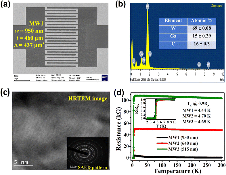 |
| | Fig. 1 The structural details and superconducting transition of MW wires fabricated using the FIB technique. (a) The SEM image of the MW1 wire, which has the width (w) of ∼950 nm and length (l) of 460 μm, and results in an active area (A) of 437 μm2. (b) The average energy dispersive spectrum of the MW wires, which results in an elementals composition of tungsten, gallium, carbon in an approximate atomic ratio of 69%, 15% and 16%, respectively. (c) The HRTEM image and SAED pattern for the FIB-deposited W shows its crystalline nature. (d) The measured resistance-temperature characteristics [R(T)] at an applied current of 100 nA in the range of room-temperature (300 K) to 2 K (in the main panel of figure) for all of the MW wires. The inset of (d) shows the R(T) characteristics in the temperature range of 10 K to 2 K for all of the MW wires. We pointed out the superconducting transition temperatures of 4.44 K, 4.7 K and 4.65 K for MW1, MW2 and MW3, respectively, which were measured at the 0.9RN at 8 K temperature. | |
Results
Structural analysis and superconducting transition of MW wires fabricated using FIB techniques
Fig. 1(a) shows the FESEM image of one of the MW (MW1) wires, which has the width (w) of ∼950 nm and length (l) of ∼460 μm, resulting in an active area (w × l) of 437 μm2. The widths and areas of all other similar (MW) devices are also mentioned in Table 1. It should be noted that a thickness of ∼80 nm was retained for all MW wires. Since, the FIB-deposited tungsten1–5 wires or films are an alloy form with compositions of different elements, like gallium (Ga) and carbon (C). The elemental compositions of these MW wires were analyzed in situ via the available energy dispersive spectrum (EDS) technique. The average EDS spectrum for the MW wires is shown in Fig. 1(b). The results showed the elemental compositions in the approximate atomic ratio of 69 ± 0.08% for W, 15 ± 0.29% for Ga, 16 ± 0.3% for C and a small amount of oxygen (O), which is analogous to previous works.1–5 Raman measurements for the MW samples (shown in Fig. S1(b) in ESI†) indicate the presence of tungsten carbide (WC) stretching modes with corresponding peaks at 678.6 cm−1 and 789.9 cm−1, which are comparable to earlier reports.43,44 The high-resolution transmission electron microscope (HRTEM) technique was used to determine the crystalline nature of these MW wires. The HRTEM image (at 5 nm scale) and SAED pattern for the FIB-deposited W is shown in Fig. 1(c), which shows the crystalline nature, as it shows the presence of lines (lattice fringes). Also, a HRTEM image at the 10 nm scale is shown in Fig. S1(c) (ESI†). In both HRTEM images, we have obseved the presence of defects and irregular structures. Since, FIB-fabricated W nanostructures1–9 exhibit rich superconductivity features below the temperature of 6 K, these MW wires were used for the low-temperature transport measurements. Fig. 1(d) shows the temperature-dependent resistance [R(T)] characteristics in the absence of a magnetic field for all of the MW wires. The R(T) characteristics (shown in the main panel) clearly show the non-metallic nature for all of the MW wires, in which MW1 shows the maximum increment of resistance, while cooling from 300 K to 2 K. This increment of resistance at 10 K (3845 Ω) is eight times higher than the resistance at 300 K (475 Ω) for the MW1 wire. The occurrence of such non-metallic nature may be due to the presence of impurities of carbon, gallium and formation oxides in the MW wires, which has also been explained in earlier reports2,4 for the tungsten strip and film. It is evident that the Ga+ beam plays an important role during the milling and fabrication process, and inherently causes the disordered nature of these FIB-fabricated W-nanostructures. The resistance also increases with decreasing temperature, representing the semiconducting type nature for the MW wire. The presence of WC, carbon and oxides may indicate the reasonable assumption of a semi-metallic nature of these FIB-fabricated W-wires in R(T), which further needs to be investigated. From the temperature range of 10 K to 2 K, the R(T) characteristics are plotted in the inset of Fig. 1(d), wherein the y-axis has a plot of normalized resistance (R/R8K) scale versus temperature. The existence of zero-state resistance is characterized by the superconducting transition temperature (TC), which lies below the temperature of 5 K. The TC is evaluated with a 10% drop of the normal state resistance, i.e., at the 0.9R8K for all of the MW wires. Consequently, the TC values were optimized to 4.44 K, 4.7 K and 4.65 K for MW1, MW2 and MW3, respectively (Table 1). This change in the superconducting transition is tunable with the variation of elemental composition of W and width (or area) of W films/wires.1–5,45 The values of the normal state resistance (RN) at the temperature of 8 K are also mentioned in Table 1 for all of the MW wires, which decreases with the increment in width. This variation in TC and RN has already been well reported with respect to the widths of the W1–5,45 films/wires, and is directly linked to the reduced flow path for the copper pairs with decreasing sample dimensions, which results in an enhancement of the disordered nature of FIB-fabricated W films or wire.
Room-temperature photoresponse measurements on MW wires under the illumination of laser lights of wavelengths 532 nm (visible region) and 1064 nm (NIR region) at the fixed power of 486 mW cm−2 and 18 mW cm−2, respectively
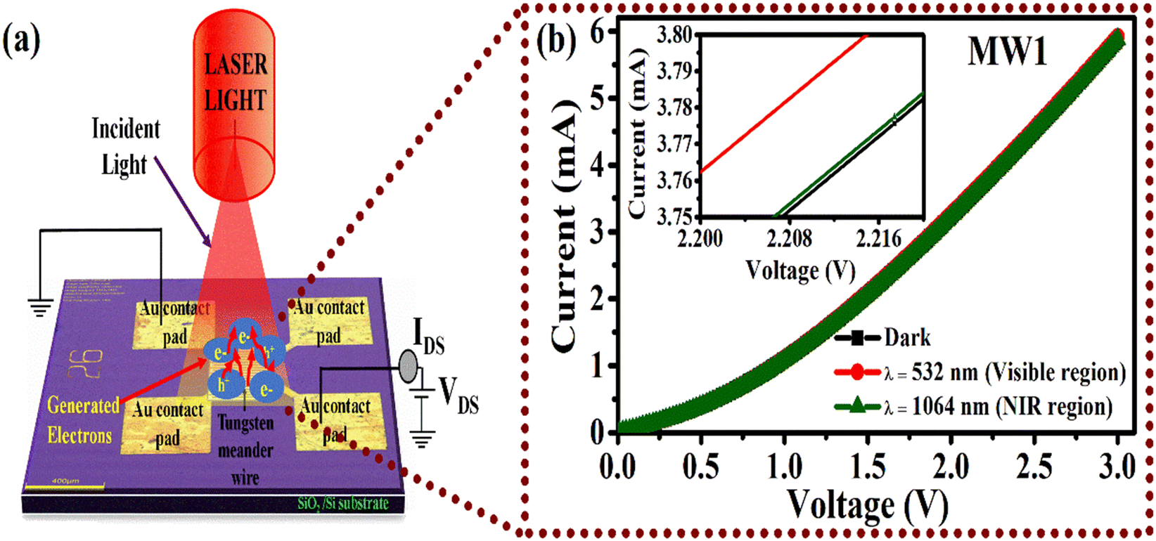
To check the applicability of these FIB-fabricated MW wires for a single photon detector, we carried out initial photoresponse measurements on these MW wires at room temperature. Surprisingly, we obtained significant photoresponsivity results. A 3D-schematic view of the used photoresponse measurement setup including the MW wire device under the illumination of a laser and the electrical connections are shown in Fig. 2(a). It should be noted that the 2-probe electrical connections were used for photoresponse measurements, which are connected to the source (current and voltage) monitoring unit. First, we recorded the channel current with and without the laser light illumination. The resultant voltage bias current response is shown in Fig. 2(b), i.e., the current–voltage characteristics (IVC) for the MW1 wire device without light (dark current with black curve) and with the illumination of laser lights of wavelength (λ) 532 nm (red curve) and λ = 1064 nm (green curve). This IVC indicates that the measured current increases with increasing bias voltage (VDS). This increment in current with VDS is due to the enhancement of the carrier drift velocity and is related to the decay of the carrier transit time (Tt), which is given by the following equation.24
where l is the length of the device and μ is the carrier mobility. In the inset of Fig. 2(b) (zoom view of main panel), the IVC isotherms clearly show the decrement in electrical resistance with the switching on the laser lights of wavelength 532 nm and 1064 nm for the MW1 wire by clearly showing the enhancement of current. Currently, we do not know the exact origin of this photoresponse feature in these FIB-fabricated MW wires. Thus, further theoretical simulations and experiments need to be performed. Since our FIB fabricated devices (MW wires) are in a meander pattern constituting a narrow path for charge carriers, this enables us to cover more surface area for absorbing more incident photons from the laser light source, playing an important role for the enhancement of photocurrent. The enhancement of current in the MW wires is due to the absorbance of photons of required energy from the laser light source. Hence, the extra charge carriers get excited, which is called a positive photoconductive effect, eventually decreasing the resistance.
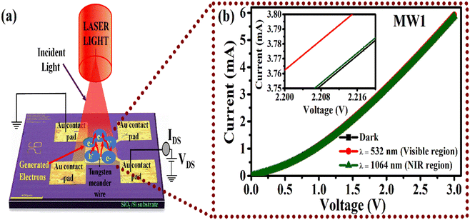 |
| | Fig. 2 Room-temperature (300 K) photoresponse measurements setup and laser light-dependent current–voltage characteristics (IVC) of the meander-structured tungsten (MW1) wire. (a) A 3D schematics view of the used photoresponse measurement setup with the assisted laser light, wherein the electrical connections are also illustrated for the photoresponse measurements on the MW wires. (b) The IVC is shown for the MW1 wire without light (dark, black curve), and when the laser lights of fixed wavelength (λ) of 532 nm of visible region (red curve) and λ of 1064 nm of the NIR region (green curve) were illuminated on the device. The IVC clearly (in inset of (b)) represents the enhancement of current (or decrement of resistance) with illumination of the laser light of different wavelengths. | |
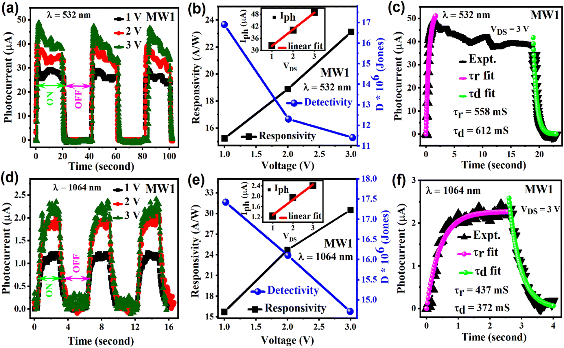
Fig. 3 displays the photoresponse features for the MW1 wire, which were measured with the applied fixed voltages under the illumination of laser lights of 532 nm (Fig. 3(a)–(c)) and 1064 nm (Fig. 3(d)–(e)) at the fixed power of 486 mW cm−2 and 18 mW cm−2, respectively. In Fig. 3, the labeled ‘ON’ and ‘OFF’ regions indicate the measurement of current in the presence and absence of laser light, respectively, which continues to the next regions in a similar manner (same for Fig. 4). The photocurrent (Iph) is calculated using the relation, Iph = Ilight − Idark, where ‘Ilight’ is the current in the presence of laser light, while ‘Idark’ is the observed current in the absence of laser light. Fig. 3(a) and (d) show the characteristics of Iphversus time, measured with fixed applied voltages of values 1 V, 2 V and 3 V for the MW1 wire. From both Fig. 3(a) and (d), it is clear that the observed photocurrent rises with the increase in the applied bias voltages. This is related to the applied bias voltage (VDS)-dependent current relationship:21
where
μ is mobility,
e is electronic charge,
w is the width, and
l is the length of the wire. This relationship indicates that
Iph is directly proportional to
VDS. We can also clearly see higher
Iph values with the illumination of the laser light of 532 nm in comparison to the 1064 nm laser light, which directly indicates that the laser light of wavelength 532 nm (of higher energy) is highly compatible in comparison to 1064 nm (of lower energy) to the energy band gap of these FIB-fabricated MW wires. The higher amount of incident energy increases the probability of absorption of incident photons to the corresponding energy band gap, which results in a greater generation of extra charge carriers,
i.e., causing the generation of a higher photocurrent. We have extracted both laser light (532 nm and 1064 nm)-dependent maximum
Iph values for the fixed applied voltages, which are plotted in the insets of
Fig. 3(b) and (e), respectively. From these figures, it is clear that
Iph increases linearly with the increment of applied voltages, which fit well with the linear equation (red curve).
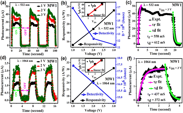 |
| | Fig. 3 Applied fixed voltages-dependent photoresponse measurements on the MW1 wire under the illumination of laser light in the visible light (532 nm) region and NIR region (1064 nm) at room temperature (300 K). (a) and (d) The generated photocurrent (Iph) as a function of time (second) at fixed voltages for the MW1 wire when the laser lights of 532 nm of fixed power 486 mW cm−2 and 1064 nm of fixed power 18 mW cm−2, respectively, are illuminated on it. The region “ON” indicated that the photocurrent is measured in the presence of laser light, while the region “OFF” indicated that the photocurrent is measured in the absence of laser light. This is continued to the next region in a similar manner. (b) and (e) The extracted responsivity and detectivity values (shown on both left and right-side Y-axis, respectively) are plotted as a function of voltage under the illumination of 532 nm and 1064 nm laser light, respectively. Insets in (b) and (e) are the plot of the voltage-dependent characteristics of Iph under the illumination of 532 nm and 1064 nm laser light, respectively, which increases linearly with the increment of voltages. This linear increment of Iph is fitted with the linear equation and is in good agreement, and the fitting is shown with a red curve. (c) and (f) The 3V–Iph (black curve) is plotted (one ON–OFF cycle only) versus measuring time from (a) and (d) under the illumination of 532 nm and 1064 nm laser light, respectively. Furthermore, the Iph of the ‘ON’ region is fitted with the rise time (τr), shown with a (pink color curve), and the ‘OFF’ region is fitted with the decay time (τd), shown with a (light green color curve). From both fittings, the measured τr and τd are of few milliseconds, which shows the fast response of the MW1 wire with the laser light. | |
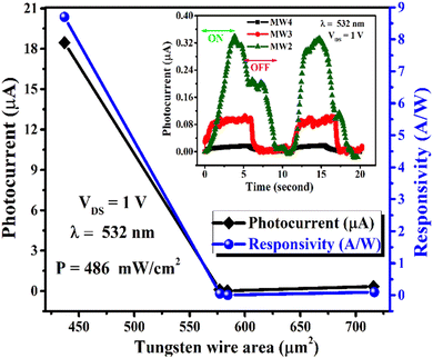 |
| | Fig. 4 MW wires area-dependent measurements of photoresponse features at room temperature (300 K). The MW wires area-dependent dynamics of the photocurrent and responsivity are shown in the main panel of Fig. 4 using a double Y-axis at the applied fixed voltage of 1 V and with the illumination of 532 nm laser light. The comparison of the generated photocurrent versus time (second) is shown in the inset of Fig. 4 for the MW wires of different areas and widths at the applied fixed voltage of 1 V with the illumination of 532 nm laser light. | |
For the evaluation of the photoresponse performance in the FIB-fabricated MW wire, we can extract the critical parameters, such as the photoresponsivity (Rph), detectivity (D), and external quantum efficiency (E.Q.E.). Here, Rph is defined as the ratio of Iph to the incident illumination power of laser light on the effective area (A), and can be expressed in the form of eqn (1):21
| | 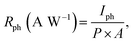 | (1) |
where,
P is the power density of the used laser light. Furthermore, using the values of
Rph, we can calculate the values of
D and E.Q.E. with the following equations:
21–24| |  | (2) |
and
| | 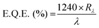 | (3) |
respectively.
Where, Idark is the current in the absence of laser light, e is the electronic charge, and Rλ is the responsivity for the specific wavelength (λ) of the laser light. From the laser light of 532 nm and 1064 nm-dependent Iph values, we calculated the values of Rph and D using eqn (1) and (2), respectively, for the applied fixed voltages for the MW1 wire. The values of extracted Rph (left Y-axis) and D (right Y-axis) are plotted using the double Y-axis in the main panel of Fig. 3(b) and (e). The Rph increases with the increment of voltage, while the D decreases. We have calculated the highest Rph values of 23.11 A W−1 and 30.51 A W−1 at the applied fixed voltage of 3 V under the illumination of laser lights of 532 nm and 1064 nm, respectively, for the MW1 wire. Also, the highest value of D is calculated to be 16.9 × 10⁶ Jones and 17.5 × 10⁶ Jones at the applied fixed voltage of 1 V under the illumination of laser lights of 532 nm and 1064 nm, respectively, for the MW1 wire. Furthermore, the highest E.Q.E. value of 53.87% and 35.56% is estimated for MW1 with an applied fixed voltage of 3 V under the illumination of laser lights of 532 nm and 1064 nm, respectively. The values of R, D and E.Q.E. for the MW1 wire are also shown in Table 1. We note that at the applied bias voltage of 3 V, the Rph value for MW1 is higher with the illumination of 1064 nm laser light in comparison to the 532 nm laser light, which can be related to the power density of the illuminated laser light. From eqn (1), it is clear that Rph is inversely proportional to the power density, which results in lower responsivity for the MW1 wire under the illumination of 532 nm laser light at the power of 486 mW cm−2 in comparison to the 1064 nm laser light at the power of 18 mW cm−2. Furthermore, the comparison of D and E.Q.E. can also be related to the Rph for the MW1 wire under the illumination of different laser lights. From the Iph characteristics as a function of time, we clearly see the increment of Iph when the laser light is ‘ON’ and decrement of Iph when the laser light is ‘OFF’. Here, the function ‘time’ can be evaluated with the rise time (τr) and decay time (τd) for the ON and OFF regions, respectively, using the following eqns.:
and
where,
t is the measuring time and
I0 and
I1 is the current constants. We have plotted the single ON–OFF cycle of
Iph (as shown by black curves in
Fig. 3(c) and (f) for the MW1 wire under the illumination of laser lights of 532 nm and 1064 nm, respectively) at an applied fixed voltage of 3 V. We have also fitted this data using
eqn (4) and (5) for the evaluation of the rise time (
τr) for the ON region and decay time (
τd) for the OFF regions, respectively. The results are in good agreement with the experimental data, shown by the pink color and light green color curves for
τr and
τd, respectively, in both
Fig. 3(c) and (f). The fitted values of
τr and
τd are 558 millisecond and 612 milliseconds, respectively, for the MW1 wire under the illumination of laser light of 532 nm, while the fitted value of
τr and
τd are 437 millisecond and 372 milliseconds, respectively, under the illumination of laser light at 1064 nm. These observed rise time and decay time values indicate the fast response of the MW1 device with respect to the laser light.
Stability features and area-dependent dynamics of the photoresponse performance of the MW wires after six months at room temperature (300 K)
In order to study the stability of the photoresponse performance on these MW devices, we investigated the devices after six months and after performing low temperature measurements. The photoresponse results are shown in Sections S2 and S3 of the ESI† with the illumination of laser lights of both 532 nm and 1064 nm wavelength, respectively, at room temperature (300 K) only for the MW1 wire. For the evaluation of the photoresponse performance after exposure to ambient conditions, we calculated the highest value of Rph (8.7 A W−1), D (12.9 × 10⁶ Jones) and E.Q.E. (20.28%) using eqn (1)–(3), respectively, at the applied fixed voltage of 1 V under the illumination of 532 nm laser light with a fixed power density of 486 mW cm−2. These values of Rph, D, and E.Q.E. were lower than previously measured results, as shown in Table 1. Furthermore, the rise (τr) and decay time (τd) constants are found to be ∼1235 and 789 milliseconds, respectively. The values of τr and τd are higher than previously measured values. Comparatively, the measured highest values of Rph, D and E.Q.E. are 10.92 A W−1, 16.2 × 10⁶ Jones and 12.72%, respectively, for the applied fixed voltage value of 1 V under the illumination of 1064 nm laser light at a fixed power of 18 mW cm−2. Using eqn (4) and (5), we fitted the τr and τd values of 1286 millisecond and 718 milliseconds, respectively, for the MW1 wire. These values are also higher than those measured previously for the MW1 wire under the illumination of 1064 nm laser light. The photoresponse features were also measured for the MW1 wire with the variation of power densities of the 1064 nm laser light at the fixed bias voltage of 500 mV. The results are shown in Section S4 of the ESI,† wherein the characteristics of Iph are plotted in Fig. S4(a) (ESI†) as a function of time and the extracted Iph and Rph values are plotted in Fig. S4(b) (ESI†). We clearly see the enhancement of Iph and Rph with the rise in power density of the 1064 nm laser light, which suggests a higher charge carrier generation with the higher power intensity. In addition, we have compared the obtained results (after 1 year) of photocurrent for the MW1 wire under the illumination of different sources, such as a Halogen light, and 532 nm, 1064 nm, 1550 nm wavelength lasers at the highest power, which are plotted in Fig. S5 of the ESI.† Fig. S5 (ESI†) clearly shows the enhancement of the photocurrent with the increment of the incident energy (or decrement in wavelength). Thus, these obtained results further show very good stability even after approximately 1 year with the broad spectral range.
Furthermore, photoresponse measurements were taken for other MW wire devices at 300 K, which have the higher area than the MW1 wire. The areas and widths of other MW samples are also mentioned in Table 1. Here, we observed that the MW2 (716 μm2), MW3 (577 μm2) and MW4 (584 μm2) devices are photoresponsive only for the laser light of 532 nm wavelength (visible regions). The absence of photoresponse features under the illumination of 1064 nm laser light indicates that the generated photocurrent is also dependent on the area and width of the nanowires. The measured Iph characteristics are shown in the inset of Fig. 4 for all of the other MW wires, which were measured at an applied fixed voltage of 1 V under the illumination of 532 nm laser light at the fixed power of 486 mW cm−2. The Iph is shown by the green, red and black curves for the MW2, MW3 and MW4 wires, respectively, as a function of time. From the inset, it is clear that the observed Iph values decrease with increasing the area of the MW2, MW3 and MW4 wires. The measured highest photocurrents are also plotted as a function of the MW wire area in the main panel of Fig. 4, on the double Y-axis scale. On the other Y-axis, the calculated Rph is plotted. It also decreases with increasing area of MW wires, which follows eqn (1) of responsivity. Using eqn (2) and (3), we estimated the values of D and E.Q.E. for all MW wires, and the results are shown in Table 1. The values of D and E.Q.E. also decrease with a decrement in the widths of the MW wires. This suggests that a good photoresponse can be observed with a MW wire of lower area and higher width. The enhancement of photoresponse features is due to the higher width of the MW wires, wherein the sample size tends toward bulk contributions.24,25,46 Hence, more charge carriers get excited/generated. Meanwhile, on lowering the MW wire width, the sample leads to the quantum size effect and the charge carriers get affected by a small channel for flow. Consequently, the resistance increases and photocurrent decreases in the MW wire of lower width. The abovementioned same hypothesis of increase in the photocurrent due to the bulk contribution has been accepted in earlier studies for the topological insulator,22,23 semiconductors,25 and others.
In summary, we found a slight degradation of the photoresponse performance of MW wires. However, we observed a significant stability even for a long time (six months to one year) duration, which is very much sought for future nanotechnology-based device development. Herein, we have clearly shown the favorable results of photoresponse properties at applied fixed voltages and at different power densities even though the device was exposed to ambient conditions. These results suggest the significant capability and stability for these FIB-fabricated MW wires in terms of technological applications.
Discussion
Earlier reports38–42 on superconducting tungsten (W) films suggest that W has a significant capability to be used for single photon detector38,39 and bolometer/transition edge sensor40–42 applications. In one of the reports, Lita et al.38 demonstrated that the photon detection efficiency of W films was close to 95%. However, these applications are limited because of the very low temperature cryogenic operation (∼100 mK range) of the W-films. FIB fabrication of tungsten film/nanowires (which have a TC ∼ 5 K) provides a platform for the higher temperature range applications in comparison to mK. This significantly motivated us to study their photoresponse features, and further its applicability to single photon detectors, bolometers, and other devices. Usually, the meander structures of nanowires are accounted for in the single photon studies,10,11,31 as these structures provide more laser light illuminated surface area with a long channel of lower width for the charge carriers, which absorbed more photons, i.e., results in the enhancement of photoresponse features. For the present study, the meander structured tungsten (MW) wires of different widths have been fabricated using the FIB technique for the investigations of their photoresponse features. Surprisingly, the performed experiments at room-temperature (300 K) indicate the significant feature of positive photoconductivity (PP) in these FIB-fabricated MW wires under the illumination of laser light of wavelength 532 nm and 1064 nm. Particularly, the observed current increases due to enhancement of the extra charge carrier generation by absorbing photons under the illumination of laser light, defined with positive photoconductivity (PP) mechanism.47–51 The most well-defined fact of PP origin in the optical performance of a material is related to the presence of energy band gap between the valence and conduction band, wherein the charge carriers are excited due to the higher incident energy with the illumination of laser light than the energy band gap of the material. The observed PP mechanism in most of the nanostructures also is originated/enhanced through the surface plasmonic effects,52–58 in which the laser light-induced excited or generated charge carriers collectively rise with the increment of the photocurrent. In comparison to PP, if the photocurrent decreases under the illumination of laser light, it is usually explained by the negative photoconductivity (NP). Depending upon the nature/type of nanodevices, in the presence of charge trapping centers,52,53 defects,54 surface plasmon polaritons,55,56 the thermoplasmonic effect,57 and the photon assisted electron–phonon scattering mechanism58 cause the decrement in laser light-induced photocurrent or negative photoconductivity. In an earlier report, the superconducting niobium-nanostructured thin film58 was used for the room temperature photodetection. In this study, the author observed the NP and this mechanism was based on the photon-assisted electron–phonon scattering mechanism. On the contrary, we observed PP in MW wires, and its mechanism is explained in following section.
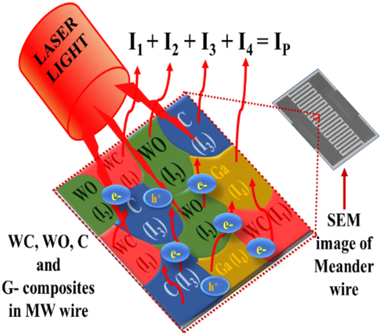
Since, these results on the PP features are new and complicated in these MW wires, the possible reasons for the generation of PP can be understood with the help of experiments. These experiments are related to the elemental composition (complex nature of composite materials, such as tungsten carbide, tungsten oxides, carbon compositions and the presence of gallium ions). Since, the earlier reports1–5 on the FIB-fabricated tungsten-nanostructures suggested that their structures are in the form of a compound or hybrid (presence of different elemental compositions of Ga (10–20%), C (15–40%) and O (<10%), in addition to W (40–60%)) due to the use of the W(CO)6 precursor and Ga ion beam, i.e., these are not fully metallic in nature.4 In our case, these FIB-fabricated MW wires have the elemental composition (as shown in Fig. 1(b)) of W, Ga, and C in an approximate ratio of 69%, 15%, 16%, respectively, including a small amount of oxygen. The process of fabrication (deposition and milling) using FIB allowed for the different elemental phase formations, such as tungsten carbide composites (WC), tungsten oxide composites (WO), and carbon compositions (C) in the tungsten-nanostructure. These phases of WC, WO, C and others have been analyzed by N. Sharma et al.,59 using XPS analysis in FIB-deposited tungsten. We have also analyzed WC phases in our case using Raman measurements, shown in Fig. S1(b) of ESI.† The category of such material composites, like tungsten carbides,48,60 tungsten oxides,28,29,61–63 carbon based nanostructures30–32 and in a confined gallium,64 have already been investigated experimentally for their intrinsic photoresponse features, which exhibited good features of positive photoconductivity by different mechanisms. It has been well reported48,60 that the WC nanoparticles show the positive photoresponse features due to localized surface plasmonic effects. Also, depending on the fabrication process, the WC phases65–67 have an inhomogeneous distribution, uncontrollable size and high electronic conductivity, which causes its further use for the efficient photocatalytic applications.50,68 On the other hand, the tungsten oxides are metal oxide semiconductors, having band gaps of ∼2.6 eV to 3 eV,28,29,69 which also shows the PP features. Also, photoconductivity features have been widely investigated in semiconducting-carbon based composites30–32 for the application of photodetector and bolometric response. In one of the reports,70 it is also claimed that the implantation of gallium ions (Ga+) enhanced the process of the charge carriers’ generation at the surface sites, resulting in the enhancement of photocurrent in the wires. Here, the Ga+ provide enhancement of the interfacial charge transfer mechanism,70 playing a crucial role for fast charge transfer, which strongly neglects the electron trapping and recombination effect. Similarly, in another work,71 a metallic rubidium silver iodide (RbAg4I5) film was coated on a gold (Au) film. Herein, the Au+ has a significant influence in the photocatalytic activity, and causes a dynamic change in the photoresponse features due to excited surface plasmon polaritons. A fast mechanism has been obtained in earlier work,50 in which the tungsten oxide–graphene heterostructure was reported to have three times higher order magnitude of photoresponse features. In this study, the semiconducting nature of tungsten suboxide plays an effective role for increasing the PIHET mechanism, achieving fast photoelectric conversion with changing the photon energy limit with respect to the band gap. From an earlier report,54 it is clear that because of the intercalation of different materials, the formed composite may also have the features of individual material and combined. So, on the basis of the above discussion, we are suggesting that the origin of photoresponse features in these FIB-fabricated MW wires is due to different complex composites of W, O, C, and Ga elements, such as WC, WO, C and others. For a better understanding, we have labeled Fig. 5 with the possible different microstructure's region of WC, WO, C and Ga mentioned by different color regime. The availability of such composites on the device surface sites causes the PP mechanism via surface plasmonic effects. The current flow resumes via intrinsic connection of the microstructure's boundaries of these composites of WC (I1), WO (I2), C (I3), and Ga (I4). Under the illumination of laser light, the photons get absorbed by these composites and results in the increment of extra charge carriers, i.e., generation of photocurrent. In the measurement of currents, the collective sum (I1 + I2 + I3 + I4) of photocurrents due to plasmonic effect, enhance the resultant photocurrent (IP) for all the wires as shown in Fig. 5. Thus, we get the results of positive photoconductivity for all of these FIB fabricated MW wires.
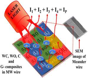 |
| | Fig. 5 Photocurrent generation mechanism in FIB-fabricated MW wires. The composites of WC, WO, C and Ga have their intrinsic nature (usually semiconducting) for exhibiting photoresponse features. In combination, these composites WC (I1), WO (I2), C (I3) and Ga (I4) resulted in the collective photocurrent (IP) via plasmonic effects in FIB-fabricated MW wires under the illumination of laser light. | |
Some photoresponse feature mechanisms are mentioned in Table 2 for the metallic composites and W, C based composites, which support our photoresponse feature observations in MW wires. In the previous reports,72,73 the authors found the topological semimetal state in tungsten carbide single crystals, and further observed superconductivity72,74 by introducing metal contacts. The topological effects in semimetals provide various features, such as dissipation-less conducting channels75,76 shift current response77,78 control mechanism on helicity of the light79,80etc. which directly enhance the photodetection mechanism.
Table 2 Details of metal-composite nanostructures and other W, C, Ga material composites with their photoconductivity mechanisms
| Material |
Positive/negative photoconductivity (PP/NP) |
Mechanism of photoconductivity |
Ref. |
| ZnO/NiO (UV photodetector) |
PP |
Semiconducting nature of material |
33
|
| TiO2/BaTiO3 (UV photodetector) |
PP |
Semiconducting nature of material |
34
|
| p-Type polyaniline polymer/ZnO (UV photodetector) |
PP |
Semiconducting nature of material |
35
|
| Metallic tungsten carbide nanoparticles |
PP |
Localized surface plasmon resonance |
48
|
| Metallic nanofibers |
PP/NP |
Surface plasmon polaritons coupling and dipole–dipole interaction coupling. |
49
|
| Tungsten oxide–graphene heterostructures |
PP |
Fast photoresponse due to plasmon induced hot-electron transfer (PIHET) |
50
|
| Au–silica nanowires (metal–semiconductor) |
PP |
Surface plasmon resonance effect |
51
|
| Metallic Pb1−xEuxTe epitaxial film |
NP |
Semiconducting nature of individual material (PbTe, EuTe) and disorder effect |
54
|
| Metallic Ag nanowire |
NP |
Surface plasmon polaritons |
55
|
| Au nanowires |
NP |
Thermoplasmonic effect |
56
|
| Nanostructured Nb thin films |
NP |
Photon assisted electron–phonon scattering mechanism |
58
|
| Tungsten carbide (WC) |
PP |
Semiconducting nature of WC |
60
|
| Tungsten oxide film (WOX) |
PP |
Semiconducting nature of WOX |
61
|
| WO3-based heterostructures |
PP |
Semiconducting nature of WOX |
62
|
| Ge-doped WOX film |
PP |
Semiconducting nature of WOX |
63
|
|
FIB fabricated tungsten wires
|
PP
|
Intrinsic nature of different composites/phases (WC, WO, C, and Ga)
|
Our work
|
Such definitions of topological semimetal state need a number of experiments and crucial analysis for the FIB-fabricated tungsten wires. The actual crystal structure is still a matter of debate for FIB-fabricated wires, as some reports suggest the amorphous,1,2 while others are of crystalline nature,7,81 which may differ by the amount of impurities/contamination during the growth process. From the TEM analysis (shown in Fig. 1(c) and Fig. S1(c) of ESI†), we result the crystallinity nature of these FIB fabricated MW wires. So, here the crystallinity nature of wires can be accounted for the enhancement of photoconductivity, as this reduces charge carrier collisions in the channel during the flow of current. Also, the presence of defects can be clearly seen in particular region (HRTEM image) for the wire. The presence of vacancies in the form of defects on surface sites, influence the relaxation mechanism of photoexcited charge carriers resulting in the enhancement of photoconductivity.82,83 The defect-induced photoconductivity can be investigated through the nanoscale mapping experiments of localized charge trap states in the grain structures.84 Based on the above discussion, it can be noted that these FIB-fabricated MW wires have significant photoresponse features at room temperature. Future studies will include the temperature-dependent photoresponse measurements on these FIB-fabricated MW wires to evaluate their applicability for single photon detection and bolometric device applications.
Conclusions
In conclusion, the tungsten wires were fabricated in meander (MW) form using focused ion beam technique, and had the different elemental compositions of tungsten, gallium and carbon in the approximate ratio of 69%, 15% and 16%, respectively. These MW wires were investigated for their distinguished superconducting properties, which showed superconducting transition temperatures near ∼4.5 K. We also studied the photoresponse properties of these MW wires under the illumination of a Halogen light and laser lights of wavelengths at 532 nm, 1064 nm and 1550 nm at room temperature (300 K). The photoresponse performance shows a significant amount of enhanced photocurrent, which leads to higher responsivity and detectivity for MW wire of higher width in comparison to lower width. We also analyzed the stability features of the broad spectral photoresponse performance after a long time. Results showed very good stability features from a technological point of view. Future studies will involve optimization of these FIB-fabricated MW wires for temperature-dependent photoresponse properties, which may result in their applicability for bolometric application. In summary, this whole study gives direct motivation to further investigate MW wires for applications in single photon detection, bolometrics and optoelectronics at room temperature and low temperatures as well. MW could play an important role in the future in optical, telecommunication devices and other technologies.
Conflicts of interest
There are no conflicts to declare.
Acknowledgements
A. K. acknowledges Dr R. P. Aloysius for help and support to carry out this work. A. K. and A. P. acknowledge UGC and CSIR, India, respectively, for providing a Senior Research Fellowship (SRF). The authors acknowledge UGC-DAE CSR, Indore, India for providing the PPMS facility. The authors acknowledge the facilities from CSIR – NPL, New Delhi and the Director for his eminent support.
References
- E. S. Sadki, S. Ooi and K. Hirata, Focused-ion-beam-induced deposition of superconducting nanowires, Appl. Phys. Lett., 2004, 85, 6206–6208 CrossRef CAS.
- Y. Sun,
et al., Voltage-current properties of superconducting amorphous tungsten nanostrips, Sci. Rep., 2013, 3, 2307 CrossRef PubMed.
- R. P. Aloysius,
et al., Superconducting properties of tungsten nanowires fabricated using focussed ion beam technique, Nanotechnology, 2019, 30, 405001 CrossRef CAS PubMed.
- P. Orús, V. M. Fomin and J. M. De Teresa,
et al., Critical current modulation induced by an electric field in superconducting tungsten-carbon nanowires, Sci. Rep., 2021, 11, 17698 CrossRef PubMed.
- K. Abhishek,
et al., On the switching current and the re-trapping current of tungsten nanowires fabricated by Focussed Ion Beam (FIB) technique, Eng. Res. Express, 2021, 3, 025017 CrossRef.
- I. Guillamón, H. Suderow and A. Fernández-Pacheco,
et al., Direct observation of melting in a two-dimensional superconducting vortex lattice, Nat. Phys., 2009, 5, 651–655 Search PubMed.
- R. Cordoba,
et al., Vertical Growth of Superconducting Crystalline Hollow Nanowires by He+ Focused Ion Beam Induced Deposition, Nano Lett., 2018, 18, 1379–1386 CrossRef CAS PubMed.
- J. Wang, M. Singh and M. Tian,
et al., Interplay between superconductivity and ferromagnetism in crystalline nanowires, Nat. Phys., 2010, 6, 389–394 Search PubMed.
- R. Córdoba,
et al., Three-Dimensional Superconducting Nanohelices Grown by He+-Focused-Ion-Beam Direct Writing, Nano Lett., 2019, 19, 8597–8604 CrossRef PubMed.
- C. M. Natarajan,
et al., Superconducting nanowire single-photon detectors: physics and applications, Supercond. Sci. Technol., 2012, 25, 063001 CrossRef.
- F. Ceccarelli, G. Acconcia, A. Gulinatti, M. Ghioni, I. Rech and R. Osellame, Recent Advances and Future Perspectives of Single-Photon Avalanche Diodes for Quantum Photonics Applications, Adv. Quantum Technol., 2021, 4, 2000102 CrossRef CAS.
- T. J. Blom, T. W. Mechielsen, R. Fermin, M. B. S. Hesselberth, J. Aarts and K. Lahabi, Direct-Write Printing of Josephson Junctions in a Scanning Electron Microscope, ACS Nano, 2021, 15, 322–329 CrossRef CAS PubMed.
- B. Bhattacharyya, V. P. S. Awana and T. D. Senguttuvan,
et al., Proximity-induced supercurrent through topological insulator based nanowires for quantum computation studies, Sci. Rep., 2018, 8, 17237 CrossRef PubMed.
- J. Wang, C. Shi, M. Tian, Q. Zhang, N. Kumar, J. K. Jain, T. E. Mallouk and M. H. Chan, Proximity-Induced Superconductivity in Nanowires: Minigap State and Differential Magnetoresistance Oscillations, Phys. Rev. Lett., 2009, 102, 247003 CrossRef PubMed.
- D. Zhang, J. Wang, A. M. DaSilva, J. S. Lee, H. R. Gutierrez, M. H. W. Chan, J. Jain and N. Samarth, Superconducting proximity effect and possible evidence for Pearl vortices in a candidate topological insulator, Phys. Rev. B: Condens. Matter Mater. Phys., 2011, 84, 165120 CrossRef.
- I. E. Zadeh,
et al., Superconducting nanowire single-photon detectors: A perspective on evolution, state-of-the-art, future developments, and applications, Appl. Phys. Lett., 2021, 118, 190502 CrossRef.
- D. V. Reddy, R. R. Nerem, S. Woo Nam, R. P. Mirin and V. B. Verma, Superconducting nanowire single-photon detectors with 98% system detection efficiency at 1550nm, Optica, 2020, 7, 1649–1653 CrossRef.
- F. Marsili,
et al., Single-Photon Detectors Based on Ultranarrow Superconducting Nanowires, Nano Lett., 2011, 11(5), 2048–2053 CrossRef CAS PubMed.
- A. Kuzmin,
et al., Geometrical Jitter and Bolometric Regime in Photon Detection by Straight Superconducting Nanowire, IEEE Trans. Appl. Supercond., 2019, 29(1–5), 2201105 Search PubMed.
- B. Korzh, Q. Y. Zhao and J. P. Allmaras,
et al., Demonstration of sub-3 ps temporal resolution with a superconducting nanowire single-photon detector, Nat. Photonics, 2020, 14, 250–255 CrossRef CAS.
- A. Sharma, A. K. Srivastava and T. D. Senguttuvan,
et al., Robust broad spectral photodetection (UV-NIR) and ultra high responsivity investigated in nanosheets and nanowires of Bi2Te3 under harsh nano-milling conditions, Sci. Rep., 2017, 7, 17911 CrossRef PubMed.
- A. Pandey, R. Yadav and M. Kaur,
et al., High performing flexible optoelectronic devices using thin films of topological insulator, Sci. Rep., 2021, 11, 832 CrossRef CAS PubMed.
- S. Verma, R. Yadav and A. Pandey,
et al., Investigating active area dependent high performing photoresponse through thin films of Weyl Semimetal WTe2, Sci. Rep., 2023, 13, 197 CrossRef CAS PubMed.
- B. Bhattacharyya, A. Gupta, T. D. Senguttuvan, V. N. Ojha and S. Husale, Topological Insulator Based Dual State Photo-Switch Originating Through Bulk and Surface Conduction Channels, Phys. Status Solidi B, 2018, 255, 800340 CrossRef.
- R. Zou, Z. Zhang, J. Hu, L. Sang, Y. Koide and M. Liao, High-detectivity nanowire photodetectors governed by bulk photocurrent dynamics with thermally stable carbide contacts, Nanotechnology, 2013, 24(49), 495701 CrossRef PubMed.
- Xu Tengfei,
et al., Recent progress on infrared photodetectors based on InAs and InAsSb nanowires, Nanotechnology, 2020, 31, 294004 CrossRef PubMed.
- X. Zhang, H. Huang, X. Yao, Z. Li, C. Zhou, X. Zhang, P. Chen, L. Fu, X. Zhou, J. Wang, W. Hu, W. Lu, J. Zou, H. H. Tan and C. Jagadish, Ultrasensitive midwavelength infrared photodetection based on a single InAs nanowire, ACS Nano, 2019, 13(3), 3492–3499 CrossRef CAS PubMed.
- Q. Liu,
et al., Interface Nanojunction Engineering of Electron-Depleted Tungsten Oxide Nanoparticles for High-Performance Ultraviolet Photodetection, ACS Appl. Nano Mater., 2018, 1, 394–400 CrossRef CAS.
- N. Huo,
et al., Synthesis of WO3 nanostructures and their ultraviolet photoresponse properties, J. Mater. Chem. C, 2013, 1, 3999–4007 RSC.
- M. E. Itkis,
et al., Bolometric Infrared Photoresponse of Suspended Single-Walled Carbon Nanotube Film, Science, 2006, 312, 413–416 CrossRef CAS PubMed.
- H. Chen,
et al., Significantly enhanced photoresponse of carbon nanotube films modified with cesium tungsten bronze nanoclusters in the visible to short-wave infrared range, RSC Adv., 2021, 11, 39646 RSC.
- Arvind Singh, Anand Nivedan, Sandeep Kumar and Sunil Kumar, Impurity assisted hopping conduction and persistent photoconductivity in disordered carbon nanoparticle film, J. Appl. Phys., 2019, 126, 225102 CrossRef.
- Z. Zhang, Y. Ninga and X. Fang, From nanofibers to ordered ZnO/NiO heterojunction arrays for self-powered and transparent UV photodetectors, J. Mater. Chem. C, 2019, 7, 223–229 RSC.
- L. Su, Z. Li, F. Cao, X. Liua and X. Fang, Tailoring the interface assembly of mesoporous TiO2 on BTO film toward high-performance UV photodetectors, J. Mater. Chem. C, 2022, 10, 9035–9043 RSC.
- Y. H. Chen, L. X. Su, M. M. Jiang and X. Fang, Switch type PANI/ZnO core-shell microwire heterojunction for UV photodetection, J. Mater. Sci. Technol., 2022, 105, 259–265 CrossRef CAS.
- M. Freitag, T. Low and F. Xia,
et al., Photoconductivity of biased graphene, Nat. Photonics, 2013, 7, 53–59 CrossRef CAS.
- B. Zhang, T. Liu and B. Meng,
et al., Broadband high photoresponse from pure monolayer graphene photodetector, Nat. Commun., 2013, 4, 1811 CrossRef PubMed.
- A. E. Lita, A. J. Miller and S. W. Nam, Counting near-infrared single-photons with 95% efficiency, Opt. Express, 2008, 16, 3032–3040 CrossRef PubMed.
- A. E. Lita,
et al., Tuning of tungsten thin film superconducting transition temperature for fabrication of photon number resolving detectors, IEEE Trans. Appl. Supercond., 2005, 15, 3528–3531 CrossRef CAS.
- A. T. Lee and P. L. Richards, A superconducting bolometer with strong electrothermal feedback, Appl. Phys. Lett., 1996, 69, 1801 CrossRef CAS.
- A. J. Miller, S. W. Nam and J. M. Martinis, Demonstration of a low-noise near-infrared photon counter with multiphoton discrimination, Appl. Phys. Lett., 2003, 83, 791 CrossRef CAS.
- B. Cabrera,
et al., Detection of single infrared, optical, and ultraviolet photons using superconducting transition edge sensors, Appl. Phys. Lett., 1998, 73, 735 CrossRef CAS.
- F. Porrati,
et al., Artificial granularity in two-dimensional arrays of nanodots fabricated by focused-electron-beam-induced deposition, Nanotechnology, 2010, 21, 375302 CrossRef CAS PubMed.
- B. Q. Yang,
et al., Effect of substrate temperature variation on nanostructured WC films prepared using HFCVD technique, Mater. Lett., 2008, 62, 1547 CrossRef CAS.
- W. Li,
et al., Tunability of the superconductivity of tungsten films grown by focused-ion-beam direct writing, J. Appl. Phys., 2008, 104, 093913 CrossRef.
- J. Yao, J. Shao and G. Yang, Ultra-broadband and high-responsive photodetectors based on bismuth film at room temperature, Sci. Rep., 2015, 5, 12320 CrossRef CAS PubMed.
- J. Jana, M. Ganguly and T. Pal, Enlightening surface plasmon resonance effect of metal nanoparticles for practical spectroscopic application, RSC Adv., 2016, 6, 86174–86211 RSC.
- W. Huang,
et al., Metallic tungsten carbide nanoparticles as a near-infrared-driven photocatalyst, J. Mater. Chem. A, 2019, 7, 18538 RSC.
- M. R. Singh, S. Parihar, S. Yastrebov and V. Ivanov-Omskii, Photocurrent in plasmonic nanofibers, J. Opt. Soc. Am. B, 2022, 39, 248–257 CrossRef CAS.
- Y. Yu,
et al., Fast Photoelectric Conversion in the Near-Infrared Enabled by Plasmon-Induced Hot-Electron Transfer, Adv. Mater., 2019, 31, 1903829 CrossRef CAS PubMed.
- S. B. Wang,
et al., Surface plasmon resonance-induced color selective Au-peapodded silica nanowire photodetectors with high photoconductive gain, Nanoscale, 2014, 6, 1264 RSC.
- N. K. Tailor,
et al., Negative Photoconductivity: Bizarre Physics in Semiconductors, ACS Mater. Lett., 2022, 4, 2298–2320 CrossRef CAS.
- Y. Yang,
et al., Hot Carrier Trapping Induced Negative Photoconductance in InAs Nanowires toward Novel Nonvolatile Memory, Nano Lett., 2015, 15, 5875–5882 CrossRef CAS PubMed.
- M. J. P. Pirralho,
et al., Disorder effect on photoconductivity properties in metallic Pb1−xEuxTe epitaxial layers, Mater. Res. Express, 2019, 6, 025915 CrossRef.
- J.-L. Sun, W. Zhang, J.-L. Zhu and Y. Bao, Negative photoconductivity induced by surface plasmon polaritons in Ag nanowire macrobundles, Opt. Express, 2010, 18, 4066–4073 CrossRef CAS PubMed.
- M. Razeghi,
et al., Plasmon-enhanced photoresponse of single silver nanowires and their network devices, Nanoscale Horiz., 2022, 7, 396 RSC.
- J. B. Herzog,
et al., Thermoplasmonics: Quantifying Plasmonic Heating in Single Nanowires, Nano Lett., 2014, 14, 499–503 CrossRef CAS PubMed.
- S. Kazim, A. Sharma and S. Yadav,
et al., Light Induced Electron-Phonon Scattering Mediated Resistive Switching in Nanostructured Nb Thin Film Superconductor, Sci. Rep., 2017, 7, 881 CrossRef PubMed.
- N. Saharma,
et al., Multi-channel Andreev reflection in Co–W nanocontacts fabricated using focused electron/ion beam induced deposition, Nanotechnology, 2014, 25, 495201 CrossRef PubMed.
- A. Hashim, Enhanced morphological, optical and electronic characteristics of WC NPs doped PVP/PEO for flexible and lightweight optoelectronics applications, Opt. Quantum Electron., 2021, 53, 478 CrossRef CAS.
- M. Hossain,
et al., Large area planar UV-Visible photodetectors using wide bandgap WO3−δ films, Opt. Mater., 2023, 135, 113322 CrossRef CAS.
- P. Du,
et al., Synthesis of GQDs/W18O49/tetragonal WO3 homostructures for improving the photoelectric properties, J. Alloys Compd., 2020, 893, 162266 CrossRef.
- F. Ünal, Investigation of Diode Parameters of Photoconductive and Photovoltaic p-Type Si/Ge-Doped WOx Heterojunction, J. Electron. Mater., 2022, 51, 6397–6409 CrossRef.
- V. A. Fedotov, M. Woodford and I. Jean,
et al., Photoconductivity in confined gallium, Appl. Phys. Lett., 2002, 80, 1297 CrossRef CAS.
- L. Fei,
et al., Observable Two-Step Nucleation Mechanism in Solid-State Formation of Tungsten Carbide, ACS Nano, 2019, 13(1), 681–688 CrossRef CAS PubMed.
- A. Y. Liu, R. M. Wentzcovitch and M. L. Cohen, Structural and electronic properties of WC, Phys. Rev. B: Condens. Matter Mater. Phys., 1988, 38, 9483–9489 CrossRef CAS PubMed.
- A. T. Garcia-Esparza, D. Cha, Y. Ou, J. Kubota, K. Domen and K. Takanabe, Tungsten Carbide Nanoparticles as Efficient Cocatalysts for Photocatalytic Overall Water Splitting, ChemSusChem, 2013, 6, 168–181 CrossRef CAS PubMed.
- M. Zhang,
et al., Facile one-step synthesis and enhanced photocatalytic activity of a WC/ferroelectric nanocomposite, J. Mater. Chem. A, 2021, 9, 22861–22870 RSC.
- S. Wang,
et al., Advances on tungsten oxide based photochromic materials: strategies to improve their photochromic properties, J. Mater. Chem. C, 2018, 6, 191–212 RSC.
- G. J. Brown and J. A. Baker, Photoresponse of ion implanted gallium dopants in silicon, Infrared Phys., 1989, 29, 43–46 CrossRef CAS.
- Y. Liu,
et al., Broadband photoresponse based on a synergistic effect of surface ions and plasmon polaritons, J. Mater. Chem. C, 2018, 6, 1199 RSC.
- X. Y. Hou,
et al., Superconductivity induced at a point contact on the topological semimetal tungsten carbide, Phys. Rev. B, 2019, 100, 235109 CrossRef CAS.
- J. Z. Ma, J. B. He and Y. F. Xu,
et al., Three-component fermions with surface Fermi arcs in tungsten carbide, Nat. Phys., 2018, 14, 349–354 Search PubMed.
- W. Zhu,
et al., Interfacial Superconductivity on the Topological Semimetal Tungsten Carbide Induced by Metal Deposition, Adv. Mater., 2020, 32, 1907970 CrossRef CAS PubMed.
- C. Z. Chang, Zero-Field Dissipationless Chiral Edge Transport and the Nature of Dissipation in the Quantum Anomalous Hall State, Phys. Rev. Lett., 2015, 115, 057206 CrossRef PubMed.
- C. Z. Chang, Experimental Observation of the Quantum Anomalous Hall Effect in a Magnetic Topological Insulator, Science, 2013, 340, 167–170 CrossRef CAS PubMed.
- J. Ma, Q. Gu, Y. Liu, J. Lai, P. Yu, X. Zhuo, Z. Liu, J. H. Chen, J. Feng and D. Sun, Nonlinear photoresponse of type-II Weyl semimetals, Nat. Mater., 2019, 18(5), 476–481 CrossRef CAS PubMed.
- G. B. Osterhoudt, L. K. Diebel and M. J. Gray,
et al., Colossal mid-infrared bulk photovoltaic effect in a type-I Weyl semimetal, Nat. Mater., 2019, 18, 471–475 CrossRef CAS PubMed.
- F. De Juan, A. Grushin and T. Morimoto,
et al., Quantized circular photogalvanic effect in Weyl semimetals, Nat. Commun., 2017, 8, 15995 CrossRef CAS PubMed.
- Q. Ma, S. Y. Xu and C. K. Chan,
et al., Direct optical detection of Weyl fermion chirality in a topological semimetal, Nat. Phys, 2017, 13, 842–847 Search PubMed.
- R. Cordoba,
et al., Vertical Growth of Superconducting Crystalline Hollow Nanowires by He+ Focused Ion Beam Induced Deposition, Nano Lett., 2018, 18(2), 1379–1386 CrossRef CAS PubMed.
- Chandan, S. Sarkar and B. Angadi, Defects induced persistent photoconductivity in monolayer MoS2, Appl. Phys. Lett., 2021, 118, 172105 CrossRef CAS.
- H. Myeong, J. Kim, J. Y. Lee and K. D. Kwon, Defect-Induced Photoconductivity in Layered Manganese Oxides: A Density Functional Theory Study, Phys. Rev. Lett., 2008, 100, 146601 CrossRef PubMed.
- M. Yang, T. Y. Kim and T. Lee,
et al., Nanoscale enhancement of photoconductivity by localized charge traps in the grain structures of monolayer MoS2, Sci. Rep., 2018, 8, 15822 CrossRef PubMed.
|
| This journal is © The Royal Society of Chemistry 2023 |
Click here to see how this site uses Cookies. View our privacy policy here. 
 Open Access Article
 This Open Access Article is licensed under a
  ab,
Alka
Sharma
c,
Animesh
Pandey
ab,
M. P.
Saravanan
d and
Sudhir
Husale
ab,
Alka
Sharma
c,
Animesh
Pandey
ab,
M. P.
Saravanan
d and
Sudhir
Husale