
 Open Access Article
 This Open Access Article is licensed under a Creative Commons Attribution-Non Commercial 3.0 Unported Licence
Ab initio study of uniaxial strain-induced thermoelectric property tuning of individual single-wall carbon nanotubes†
Md. Mafizul
Islam
 ab and
Ahmed
Zubair
*a
ab and
Ahmed
Zubair
*a
aDepartment of Electrical and Electronic Engineering, Bangladesh University of Engineering and Technology, Dhaka 1205, Bangladesh. E-mail: ahmedzubair@eee.buet.ac.bd
bDepartment of Textile Machinery Design and Maintenance, Bangladesh University of Textiles, Dhaka 1208, Bangladesh
First published on 26th October 2023
Abstract
Carbon nanotubes (CNT) have garnered significant importance as thermoelectric (TE) material due to their high TE performance owing to their inherent fascinating one-dimensional quantum confinement of charge carriers. Among various methods to tune and enhance TE properties, the impact of strain on the properties of CNT-based TE devices is rarely explored, though it is immanently present, specifically on multi-functional CNT fibers. In this study, we present the tunability and enhancement of electronic and TE properties of single-wall carbon nanotubes (SWCNTs) by strain engineering within the framework of density functional theory and Boltzmann transport theory. Semiconducting to metallic transition with a zigzag pattern of band gap (Eg) and Seebeck coefficient (S) variation was observed for uniaxial strain due to shifting of the Dirac points. Within the smaller range of strains, the Eg and S for the (10,0) SWCNT exhibited a positive correlation with tensile strain and demonstrated a negative correlation with compressive strain, while it showed a reverse trend for (11,0) SWCNT. In contrast, for (9,0) SWCNT, the Eg and S increased under both tensile and compressive strains. The SWCNTs exhibited a significant enhancement of thermoelectric transport properties while they underwent tensile and compressive strains. Applying uniaxial stress enhanced the Seebeck coefficient of SWCNTs to 1580 μV K−1. We achieved the enhancement of thermoelectric power factor as follows: 2.2 mW m−1 K−2 (−9%), 1.3 mW m−1 K−2 (−3%), 1.15 mW m−1 K−2 (−3%), and 1.24 mW m−1 K−2 (−9%) for (6,6), (9,0), (10,0), and (11,0) SWCNTs, respectively. The overall performance parameter thermoelectric figure of merit, zT was tuned up to 1.56 when the strain varied from −9% to +9%, a fewfold increment compared to its relaxed state. The optimum range of doping for SWCNTs was found to be within 5 × 1019 cm−3– 1 × 1021 cm−3 to achieve the best thermoelectric power factor and zT. The insights gained from this study will be indispensable for diverse applications in the solid-state and especially in fiber-based wearable nanoelectronic devices such as strain sensors, thermoelectric energy harvesters, and thermoelectric coolers.
1 Introduction
The demand for wearable electronic devices such as wireless sensor networks, fiber transistors, fabric antennae, electric connectors, fiber-based circuitry, smartwatches, and health monitoring bracelets is increasing day by day.1–3 Flexible, lightweight, compact, continuous, and uninterruptible power supplies are essential for these devices.4 Conventional fuel-based non-renewable energy sources are running out quickly due to the growing demand for energy in industrial processes. The search for alternative clean and environmentally friendly energy sources is highly required to meet the growing need for a mobile electrical energy supply.5,6 However, among all the energy sources, a significant amount of energy is being wasted as heat by burning fossil fuels and other conventional and renewable sources. If this energy could be reused and turned into electricity effectively and efficiently, it would be a good potential source of electrical power.7 This problem can be solved by a solid-state thermoelectric (TE) device that utilizes the Seebeck effect to turn waste heat directly into electricity.8 Among the existing matured technologies, solid-state thermoelectric nanogenerators (TEG) have attracted much interest due to the absence of moving mechanical parts, no greenhouse gas formation, excellent stability, high dependability, and long operational life of the devices.7,9,10 Interestingly, these TE devices can convert electricity into thermal energy. They enabled cooling or heating action using the Peltier effect and thermal energy harvesting using the Seebeck effect. TEG has been an enormous application in self-powered biosensors and IoT-based devices.10–12The human body is an enormous energy source generated by body heat and the moving of organs.13 A person's daily activities, such as breathing, body heating, leg movements, finger and limb motions, may generate substantial power to make a wearable electronic device operational.12 Scientists have focused on developing solid-state energy harvesters based on the principles of piezoelectricity, triboelectricity, electrostatics, and thermoelectricity. These devices can convert mechanical or thermal energy into electric energy, referred to as nanogenerators.14–16 Among these devices, TEG converts heat into electricity and vice versa. The performance of TE materials is assessed by the thermoelectric figure of merit zT factor, which can be formulated as zT = S2σTκ−1, where S is the Seebeck coefficient, σ is the electrical conductivity, T is the average temperature between the hot and cold junction of the device and κ is the thermal conductivity of the materials. The high κ is desirable for active cooling or heating, which has tremendous potential in the thermal management of electronic systems. While low κ and high power factor, PF (S2σ) is expected for energy harvesting.17
Commercial inorganic TE materials, such as Bi2Te3, PbTe, SnSe, and their alloys have exhibited a high Seebeck coefficient and improved TE performance at room temperature.18–20 However, their limited availability, high cost, and specifically, high stiffness limit their application in wearable devices. Despite the low PF value, organic materials can be used due to being nontoxic, bendable, and cost-efficient.21 Semiconducting polymer materials exhibited modest zT values (0.1–0.42) under ambient conditions because of inherent low thermal conductivity (∼1.5 W m−1 K−1), although their PF (78–500 μW m−1 K−2) is smaller than that of commercially available inorganic TE materials.22,23 Coating inorganic TE materials on various flexible substrates is a process that is used frequently.24 Another approach incorporates bulk TE electrodes into an elastic polymer with flexible terminals.25 The final TE generator becomes stretchable, but impermeability prevents it from covering a wider body region. High-performance inorganic TE materials were blended with flexible organic-like conductive polymers.8
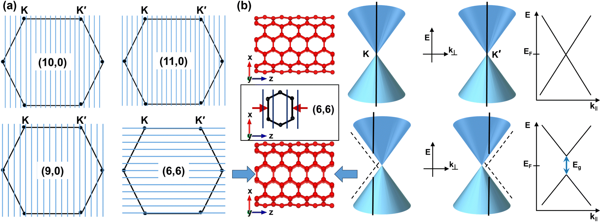
However, currently available wearable TE devices are mostly bendable rather than stretchable and compressible. Consequently, exploring novel flexible as well as stretchable and compressible TE materials is crucial in developing TE generators for self-powered wearable electronics and IoT-based devices. Carbon nanotubes (CNTs) are promising TE materials due to their favorable characteristics, such as high electrical conductivity, high thermal conductivity, high flexibility, high tensile strength, high elasticity, large aspect ratio, and light weight. Moreover, they have good electronic properties depending on their structural characteristics.26,27 Besides their intriguing attributes, CNTs can achieve enhanced TE performance through one-dimensional (1D) confinement of charge carriers leading to a confined carrier distribution channel by controlling the position of the Fermi level (EF) at the edges of the band gap, where the 1D van Hove singularities (vHs) are located in the density of states (DOS).28,29 Tuning the position of EF can be performed by adding appropriate dopants with the required concentration.17,27,30,31 The physical structure of CNT is formed by a hexagonal lattice of sp2-bonded carbon atoms, as of graphene, which is created by rolling up a monolayer graphene sheet. The structure of a single wall carbon nanotube (SWCNT) can be represented by a chiral vector, Ch ≡ na1 + ma2 ≡ (n,m) where chiral indices are represented by the integers n, m such that 0 ≤ m ≤ n and a1,a2 indicate the real space translational unit vectors. The chiral angle formed between Ch and a1 determines the electronic properties of SWCNT. Based on chirality, SWCNTs can be classified into four types. The n = m represents the armchair nanotube with metallic behavior. Another type of nanotube exhibits metallic behavior when n–m is a multiple of three. Nanotubes with chirality (n,0) represent the zigzag type, and n ≠ m is a chiral nanotube; both reveal semiconducting characteristics, except their difference is a multiple of three. CNT is a potential candidate for TE materials with diversified applications such as energy harvesters, photodetectors based on the photo-thermoelectric effect, and solid-state coolers using the Peltier effect.17,32 CNT-based composites33,34 are promising as a TE material despite their high lattice thermal conductivity, as phonon transport is suppressed by scattering at CNT-to-CNT junctions. Furthermore, the CNT film grown on different substrates is often accompanied by lattice mismatch, leading to either tensile or compressive strain. Similarly, highly aligned multifunctional CNT fiber experiences uniaxial tensile strain.35,36 However, it is crucial to comprehend the impact of strain on the TE characteristics of CNTs as they are inherently present in practical systems. The utilization of strain engineering has proven to be an effective approach to modify the physical properties of a material in a wide range of areas since strain alters the electronic band structures. Many previous studies reported the alteration of the electronic band gap of CNTs under uniaxial strain along the tube axis.37,38 Jiang et al. reported the value of Seebeck coefficient, electrical conductivity, and TE figure of merit 196 μV K−1, 11.9 MS m−1, and 0.15, respectively for p-type (10,0) SWCNT and further enhanced the TE parameters at elevated temperature with a zT value of 0.77 at 1000 K.39 Zeng et al. reported a 3.5-fold reduction in the thermal conductivity of CNT networks by defect engineering.11 The tunability of the Seebeck coefficient and electronic band gap was reported for (7,0) and (8,0) SWCNTs through uniaxial stress.40 Hence, strain is one of the methods to alter both the electronic and thermoelectric properties of CNTs and is expected to enhance the TE performance of nanomaterials. However, a comprehensive study of the impact of strain on the thermoelectric performance of CNTs is rarely explored.
In this study, we systematically analyzed the impact of strain on the electronic and TE properties, particularly the band structure (E–k), the density of states (DOS), Seebeck coefficient S, electrical conductivity σ, and TE PF of different types of SWCNTs. We simulated these properties using density functional theory (DFT) based first-principles calculations in both relaxed and uniaxially strained SWCNTs. DFT-based calculations are important techniques to determine the material's electronic properties such as band structure, density of states, binding energies of molecules or atoms adsorbed onto the surface of a material, and charge transfer between atoms.37,41,42 We utilized the Boltzmann transport theory to determine transport-related properties such as electrical conductivity, Seebeck coefficient, and thermal conductivity.17,27,39,40 By applying mechanical stress parallel to the tube axis, we achieved tunability in the band gap, S, σ, and TE PF of those SWCNTs. These findings have interesting applications in substrate-free wearable thermoelectric devices such as TEG, which can power biosensors, IoT-based devices, and wearable electronic devices. Additionally, owing to the direct band gap nature over the whole tunable range, these SWCNTs can be fabricated to substrate-supported thin film optoelectronic devices and TE coolers as thermal management of electronic devices.
2 Computational details
To determine the structural and electronic properties of SWCNTs, we conducted ab initio calculations within the DFT framework using a Quantum ESPRESSO (QE) simulation package.43 Structural optimization and physical property calculations were performed using a plane-wave basis set and projector-augmented wave (PAW) pseudopotentials. The Perdew–Burke–Ernzerhoff (PBE) exchange–correlation functional was utilized within the generalized gradient approximation (GGA). For the expansion of the plane wave, kinetic energy and charge density cutoffs were set to 45 Ry and 350 Ry with the Fermi–Dirac smearing method to achieve good convergence of the calculations. We considered three types of zigzag SWCNTs with chirality (10,0), (11,0), (9,0), and an armchair type (6,6) SWCNT. The selected SWCNTs have similar diameters. The first three SWCNTs can be generalized as (n,0) with n = 3i + j, where i is an integer, j = ±1 represents the semiconducting characteristics of SWCNT and j = 0 demonstrates the metallic behavior of SWCNT. In this study, j = +1 represents (10,0) SWCNT, j = −1 indicates (11,0) SWCNT, and j = 0 reflects (9,0) SWCNT. The initial geometries of SWCNTs were built using a structure builder code. The hexagonal honeycomb lattice structure was considered to build the SWCNT unit cell. We optimized the structures until the force on the atoms and the total energy were smaller than 0.001 Ry bohr−1 and 0.0001 Ry, respectively. The Broyden–Fletcher–Goldfarb–Shanno (BFGS) algorithm was adopted to optimize the structure. To prevent interaction between neighboring tubes, SWCNTs were deemed isolated by creating a 30 Å vacuum perpendicular to the tube axis.We modeled uniaxial strain along the tube axis (Z-axis) on the relaxed structures, which is illustrated in Fig. 1(f). The percentage of uniaxial strain (εz) was calculated by using the formula, εz = [(l − l0)/l0] × 100%, where l and l0 are the tube lengths for strained and unstrained SWCNTs, respectively. Additionally, the coordinates corresponding to the axial direction of the tube were changed accordingly to introduce strain (εz). The positive value of εz indicates tensile strain, while the negative value for compressive strain. The uniaxial strains (−9% to +9%) were introduced by applying external hydrostatic pressures along the tube axis.
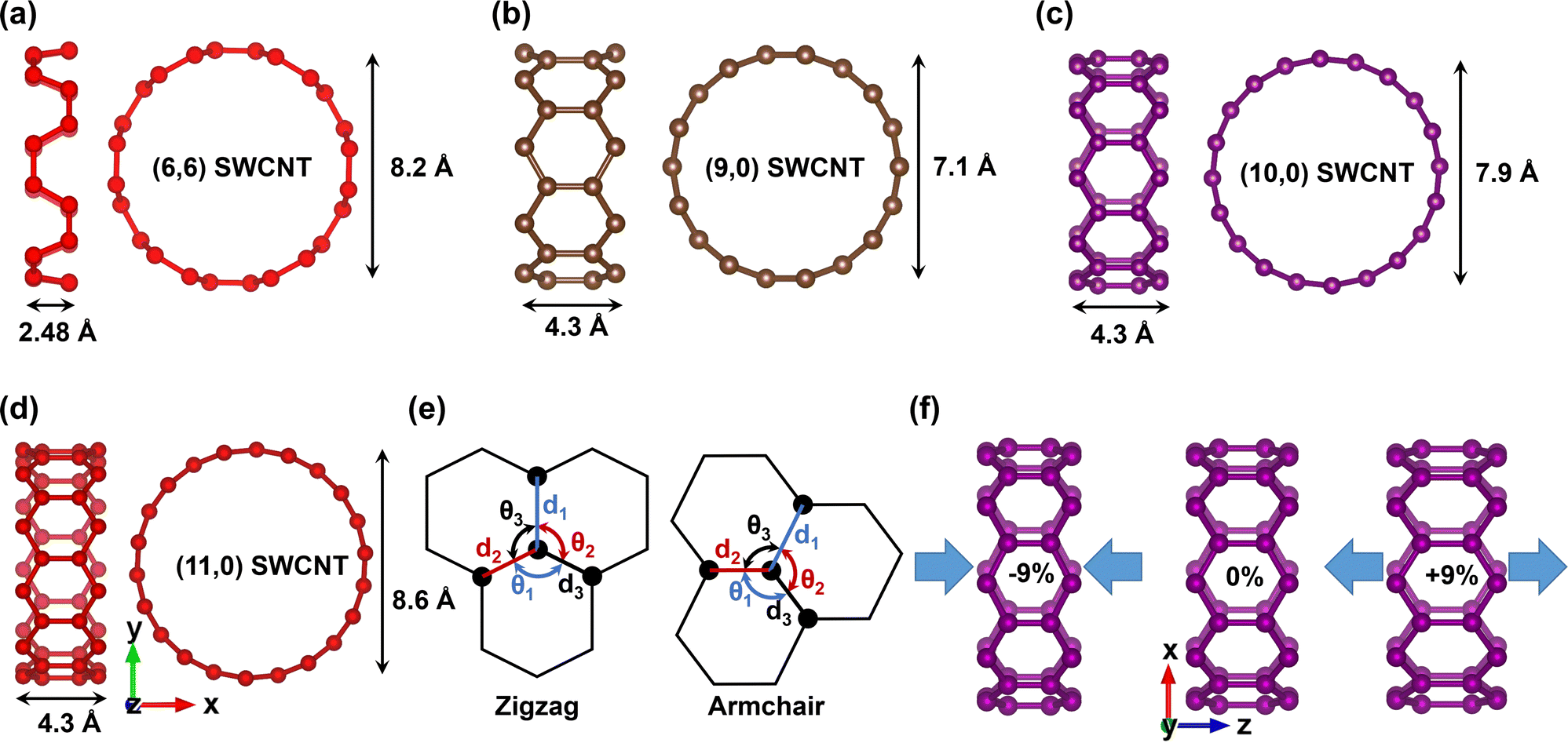 | ||
| Fig. 1 The side view (XZ) and top view (XY) of relaxed structures for (a) (6,6), (b) (9,0), (c) (10,0), and (d) (11,0) SWCNTs. (e) The schematic view of bond lengths and bond angles with denotation. (f) Illustration of uniaxial compressive strain (−9%), unstrained (0%), and tensile strain (+9%) along the tube axis. The strain illustration is shown for the (10,0) SWCNT. | ||
A gamma-centered 1 × 1 × 5 Monkhorst–Pack k-grid was incorporated into the first Brillouin zone for geometry optimization and self-consistent field (SCF) calculation. A denser k-mesh of 1 × 1 × 1000 was selected for non-self-consistent field (NSCF) calculation to obtain the electronic properties with high accuracy. The electronic band structures and DOS were calculated within the irreducible first Brillouin zone of the hexagonal k-path (Γ–M–K–Γ–A–L–H–A|L–M|K–H). To better understand the electronic property alteration with strain, we performed the projection of the atomic orbitals on the E–k plot of SWCNTs by showing the contributions of s, pz, py, and px orbitals of the constituent carbon atoms.
The calculated electronic properties were used to compute the thermoelectric characteristics of both unstrained and strained SWCNTs. The thermoelectric transport properties Seebeck coefficient S, electrical conductivity σ, TE PF, and electronic thermal conductivity κe were calculated using semiclassical Boltzmann transport theory using constant relaxation time approximation (CRTA) as implemented in the BoltzTraP code.44 The Boltzmann transport equations (BTE) were solved by interpolating the electronic energy band structures by performing the required integrations. The CRTA method is still effective for obtaining accurate results at a relatively low computational cost, despite the existence of advanced methods to calculate the relaxation time considering the scattering of phonons and ionized impurities along with the energy-momentum dependencies.45 As we qualitatively analyzed the impact of strain on the thermoelectric performance of SWCNTs, we considered a reference value of relaxation time τ = 0.8 × 10¹⁴ s.46
3 Results and discussion
3.1 Structural properties
The structure of SWCNTs were optimized until minimum ground state energies were achieved. The initial geometries of the unit cell of (6,6), (9,0), (10,0), and (11,0) SWCNTs were built containing 24, 36, 40, and 44 carbon atoms, respectively. The geometries of the unit cell of SWCNTs were relaxed until the desired threshold for total energy and force were attained. The optimized structures are shown in Fig. 1(a)–(d). The optimized diameters were 8.2 Å, 7.1 Å, 7.9 Å, and 8.6 Å for (6,6), (9,0), (10,0), and (11,0) SWCNTs, respectively. The bond lengths and bond angles are illustrated in Fig. 1(e). The C–C bond angle, θ1 just opposite to d1 was slightly smaller than θ2 and θ3 for the zigzag SWCNTs. The bond angle θ2 was higher (119.8) than θ1 and θ3 for (6,6) SWCNT. The bond lengths between the nearest carbon atoms and their bond angles for the relaxed SWCNTs are summarized in Table 1. Our optimized geometric parameters agreed well with the previously reported findings.39,41,47,48| CNT | D (Å) | d 1 (Å) | d 2 (Å) | d 3 (Å) | θ 1 | θ 2 | θ 3 |
|---|---|---|---|---|---|---|---|
| (6,6) | 8.2 | 1.428 | 1.422 | 1.428 | 119.0° | 119.8° | 119.0° |
| (9,0) | 7.1 | 1.435 | 1.425 | 1.425 | 117.4° | 119.8° | 119.8° |
| (10,0) | 7.9 | 1.431 | 1.425 | 1.425 | 117.8° | 119.9° | 119.9° |
| (11,0) | 8.6 | 1.422 | 1.429 | 1.429 | 118.0° | 120.0° | 120.0° |
We modeled uniaxial strains on the relaxed SWCNTs along their tube axial direction. To apply the mechanical strain, external hydrostatic pressures were required, which we calculated for each level of strain and we summarized the results in Table 2. According to the analyses of our calculated results, we observed that a higher level of hydrostatic pressure was required to apply strain on SWCNTs with a larger diameter. At smaller strains, the amount of hydrostatic pressure required was greater for stretching, for instance, 0.3 kbar, 0.4 kbar, 0.6 kbar, and 0.9 kbar additional pressures were required to apply 3% tensile strain compared with 3% compressive strain on (6,6), (9,0), (10,0), and (11,0) SWCNTs, respectively. In contrast, to apply larger strains, the required external hydrostatic pressure for compression was higher than stretching the SWCNTs, for example 10.9 kbar, 9.6 kbar, 10.5 kbar, and 10.9 kbar additional pressures were required to apply 9% compressive strain compared with the same level of tensile strain on (6,6), (9,0), (10,0), and (11,0) SWCNTs, respectively. At the larger level of strains, the constituting atoms of SWCNTs became loosely coupled during stretching, which is why the pressures for higher tensile strains were less than the same level of compressive strains, while during compression, the atoms became closer while tightly coupled to each other, which resulted in an increased amount of external hydrostatic pressure to apply higher compressive strains. The positive value of pressure is for compression, while the negative value indicates the stretching of SWCNTs.
| ε z (%) | P (6,6) (kbar) | P (9,0) (kbar) | P (10,0) (kbar) | P (11,0) (kbar) |
|---|---|---|---|---|
| −9 | 26.9 | 24.3 | 26.3 | 28.0 |
| −6 | 15.8 | 14.2 | 15.4 | 16.3 |
| −3 | 6.7 | 6.0 | 6.4 | 6.7 |
| +3 | −7.0 | −6.4 | −7.0 | −7.6 |
| +6 | −12.0 | −11 | −11.9 | −12.9 |
| +9 | −16.0 | −14.7 | −15.8 | −17.1 |
3.2 Modulation of electronic properties of SWCNTs by uniaxial strain
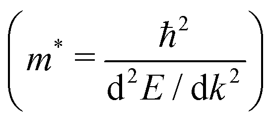
To investigate how the uniaxial strain impacts the electronic properties of SWCNTs, we calculated the electronic band structures for four different types of SWCNTs. We denoted the first allowed optical transitions for semiconducting and metallic nanotubes by S11 and M11, respectively. The calculated band gap or the first optical transition S11 for (10,0) SWCNT was 0.97 eV without strain. We introduced strain parallel to the axial direction of the tube on its relaxed structure. We found shrinking characteristics of the band gap with the application of compressive stress, and the band gap increased again followed by semiconductor-to-metal transition at a percentage of compressive strain in between 6% and 9% which can be seen in Fig. 2. On the other hand, S11 increased until 3% tensile strain with a peak value of 1.22 eV and again started to decrease. The flattened value of the band gap was obtained at both +2% and +3%, which agrees with the reported findings.49 The oscillating pattern of changing band gap with uniaxial strain is evident from the Dirac points (K and K′) shift, as can be observed in Fig. 2(h). In SWCNTs, the k lines perpendicular to the tube axis, k⊥ is quantized. However, the electrons are free to move larger distances in the direction parallel to the CNT axis, and hence, the electron wavenumber in the tube axial direction, k‖, will be effectively continuous. The continuous k‖ states in each quantized k⊥ value is a 1D sub-band, which will be represented by an allowed k line in the 2D Brillouin zone. The discrete values of k⊥ are obtained by the boundary condition,| πDk⊥ = 2πt | (1) |
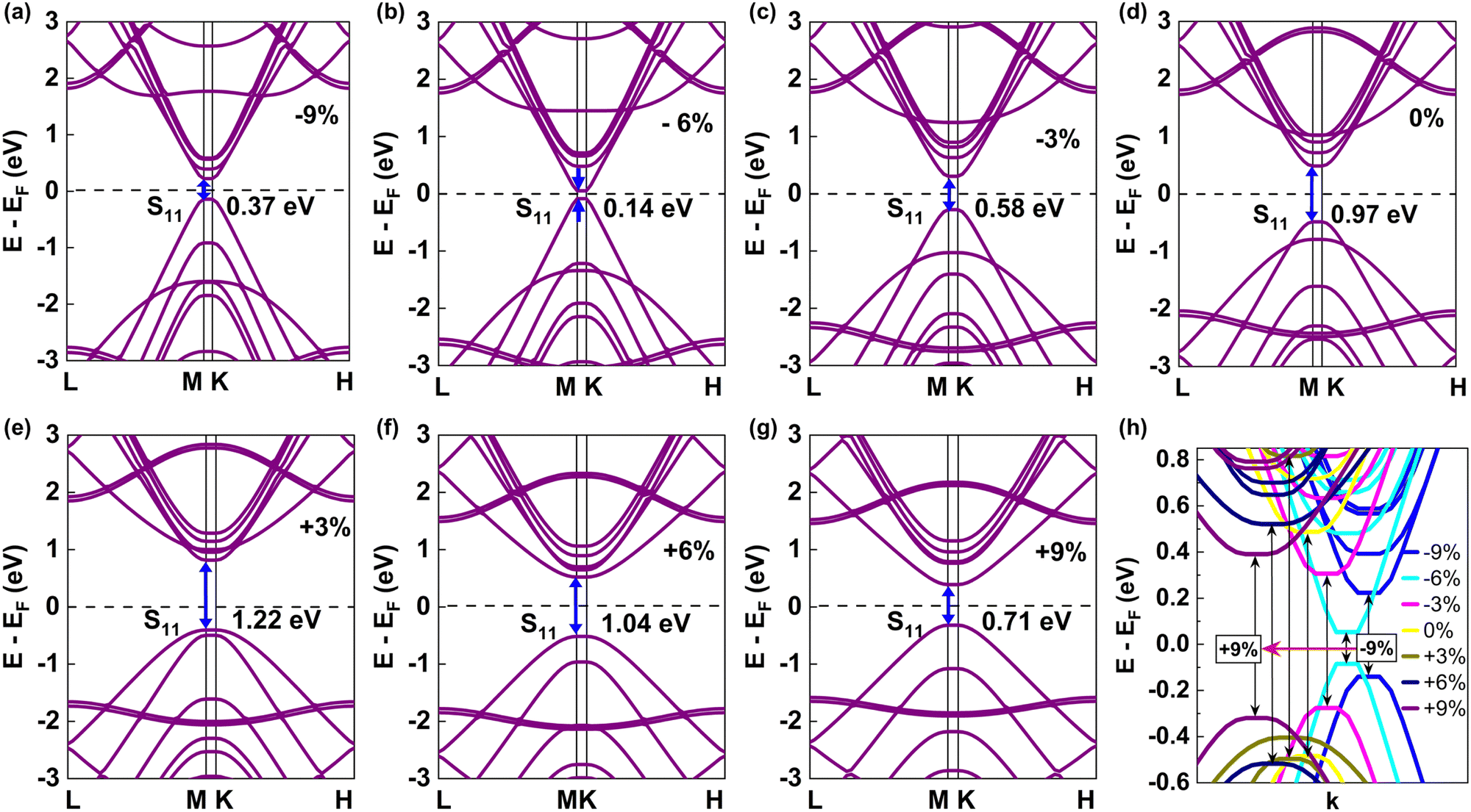 | ||
| Fig. 2 Band structures of the (10,0) SWCNT at different strains – (a) −9%, (b) −6%, (c) −3%, (d) 0% (relaxed state), (e) +3%, (f) +6%, and (g) +9%. (h) An expanded figure of conduction band minima (CBM) and valence band maxima (VBM), where the energy dispersion cones were shifted due to uniaxial strain. | ||
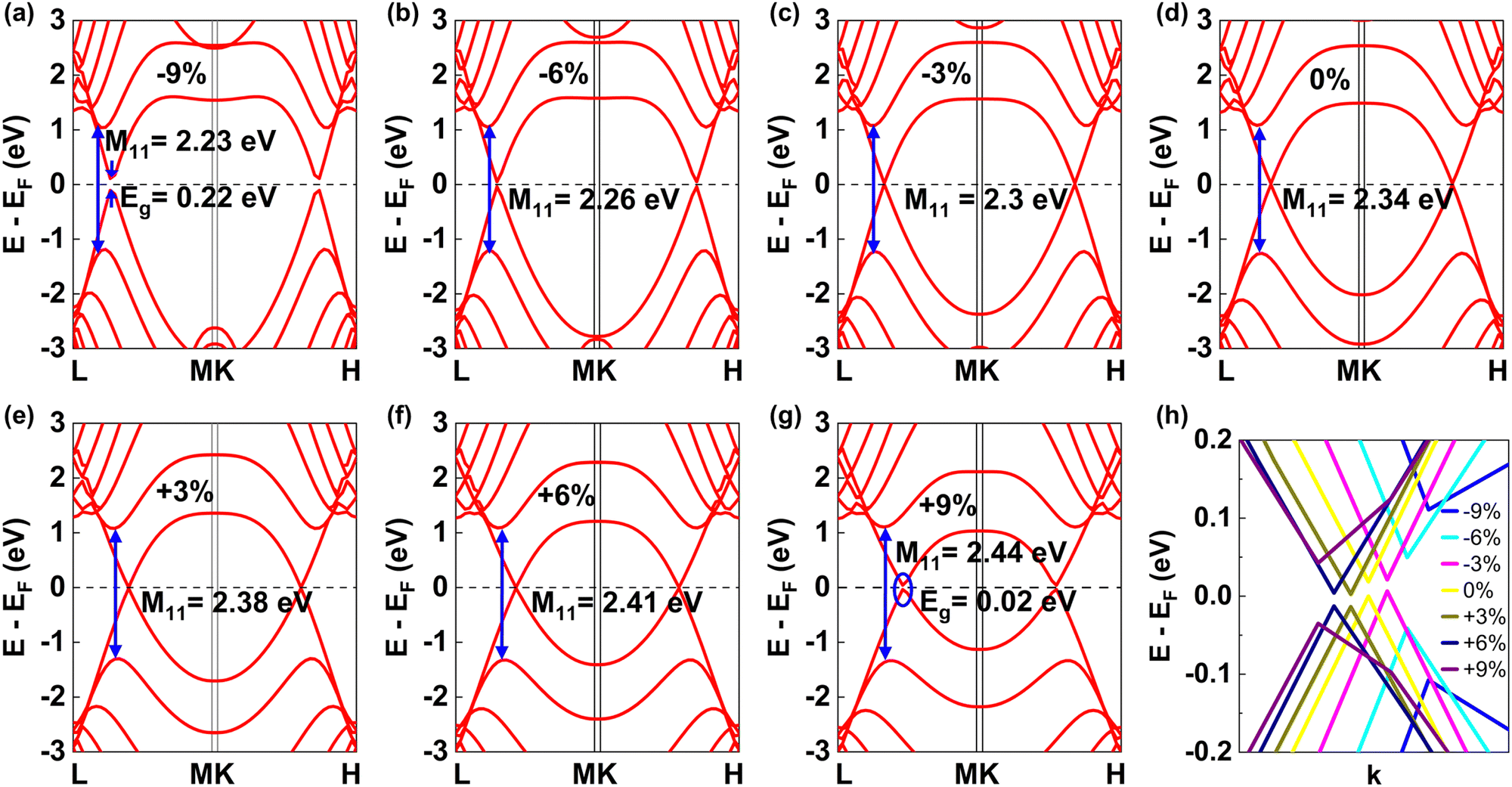
For the pristine (11,0) SWCNT, the band gap was found to be 0.8 eV, which well matched with the previous computational studies.41 The band gap variation showed a decreasing trend over −3% to +6% of strain with tunability from 1.05 eV to 0 eV, as can be seen in Fig. 4. The band structures of (11,0) SWCNT at various uniaxial strains are provided in Fig. S1 of the ESI.† Semiconductor-to-metal transition occurred at 6% tensile strain. For −9% to −3% of uniaxial strain, an opposite trend was observed. The trend of band gap variation in a zigzag pattern would be repeated above 9% of compressive strain and 6% of tensile strain. When the (11,0) SWCNT under uniaxial strain showed semiconducting behavior, it had a direct band gap. Similar to the (10,0) SWCNT, it showed narrower curvature of the bands at the CBM and VBM due to compressive strains and can be expected to have a lower effective mass with high carrier mobility for charge transport. The (10,0) and (11,0) SWCNTs both manifested semiconducting behavior with two distinct types and exhibited a reverse slope of band gap change within a narrow range of uniaxial strains (−3% to +3%), which can be seen in Fig. 4.
The impact on the electronic band structure due to uniaxial strain on the quasi-metallic (9,0) SWCNT is shown in Fig. S2 of the ESI.† The chirality of this SWCNT can be generalized as (n,0), where n is an integer multiple of 3. At a relaxed state, the (9,0) SWCNT evinced a small band gap of 0.19 eV due to the curvature effect (see Fig. S2(d) of the ESI,† which aligned well with the previously reported DFT calculations41,50 and was consistent with the experimental result.51 The band gap widened upon application of both compressive and tensile stresses, and the trend of band gap alteration obtained was similar to that reported in earlier studies.52 The opening of the band gap in both types of strains was due to the shifting of the Dirac points and k lines, which created a displacement between them.
The armchair type (6,6) SWCNT showed zero (0 eV) band gap with completely metallic characteristics under pristine conditions (see Fig. 3(d)). The band gap was not opened while the strains were within −3% to +6% along the tube axis. However, at −6% strain, it opened a very little band gap of ∼0.09 eV and increased to 0.22 eV at −9% strain as depicted in Fig. 4(a). The uniaxial strain caused a change in the position of the Dirac points (K and K′) in the hexagon, and shifted the position of the CBM and VBM (occurred at same wave vector k) in band structure (see in Fig. 3(h)). The allowed k lines that went through K and K′ points shifted away due to the application of εz on the (6,6) SWCNT as can be visualized in Fig. 3(h). Hence, a band gap opened up and increased with uniaxial strain on the armchair SWCNT.
 | ||
| Fig. 3 Band structures of the (6,6) SWCNT at different strains – (a) −9%, (b) −6%, (c) −3%, (d) 0% (relaxed state), (e) +3%, (f) +6%, and (g) +9%. (h) A zoomed-in view of the CBM and VBM, where the shiftings of Dirac cones of energy dispersion due to uniaxial strain are apparent. | ||
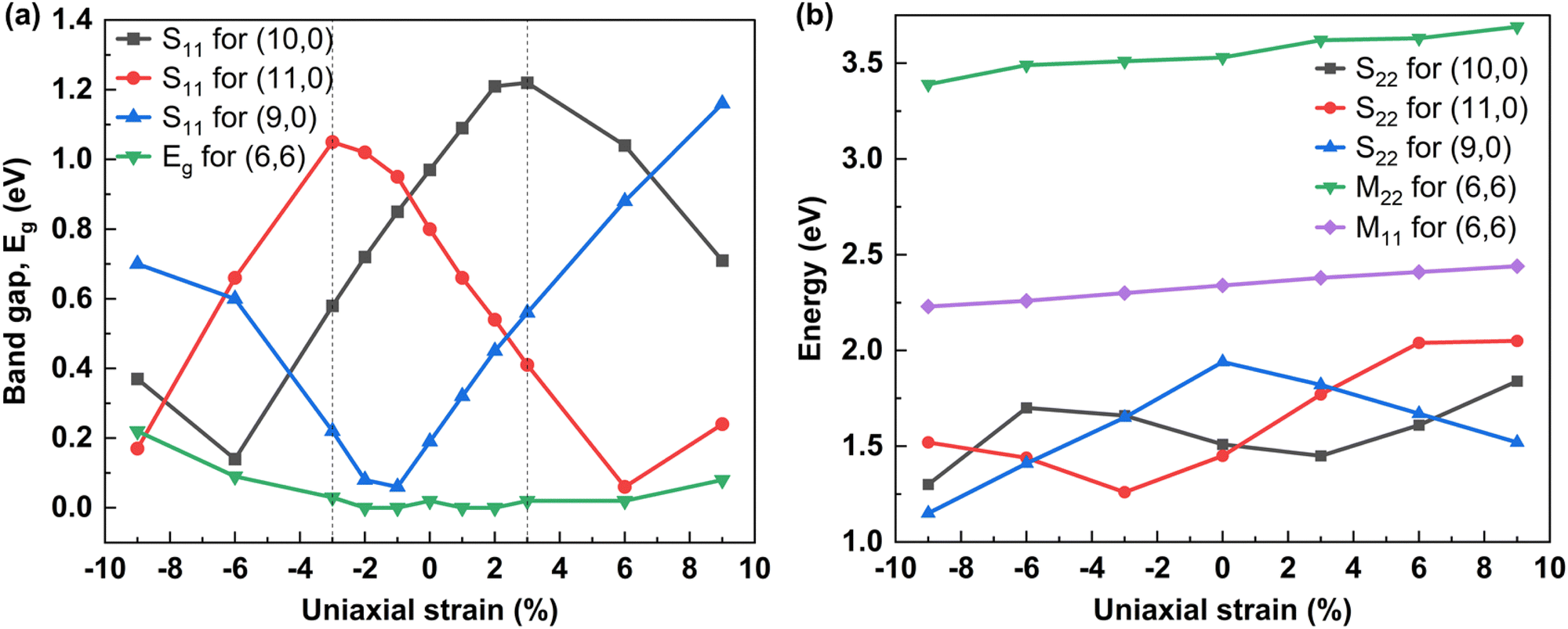 | ||
| Fig. 4 (a) Variation in band gap with uniaxial strain parallel to the tube axis for (10,0), (11,0), (9,0), and (6,6) SWCNTs. The band gap varied in zigzag patterns with strain on (n,0) SWCNTs. A band gap opened up for the purely metallic (6,6) armchair SWCNT at above 6% of compressive and tensile uniaxial strain. (b) The first sub-band optical transition energies for metallic tube, M11, and second sub-band optical transition energies (S22 and M22) variation with uniaxial strain. S22 and M22 varied following a trend opposite to band gap or S11 variation for (n,0) SWCNTs. | ||
In Fig. 4, we plotted the variation of first and second allowed optical transition energies (S11, M11, S22, M22) for all nanotubes and opened the band gap for armchair nanotubes with uniaxial strain. The (10,0) SWCNT, which lies under the (n,0) zigzag SWCNT of type n = 3i + 1, showed a positive slope of a band gap change between −6% and +3% uniaxial strain. On the contrary, (11,0) SWCNT, another type of zigzag SWCNT with n = 3i − 1 manifested a negative slope of band gap variation within −3% to +6% strains. Moreover, (9,0) SWCNT belongs to quasi-metallic type zigzag SWCNT with n = 3i that revealed a positive and negative slope of band gap alteration for tensile and compressive strains, respectively. Here, in all types of zigzag SWCNTs, the change of band gap occurred in a zigzag pattern with uniaxial strain. It can be explained through the sampling of the first Brillouin zone (BZ) by allowed cutting lines (k lines) in reciprocal space according to Fig. 5(a). The BZ of a SWCNT is a hexagon containing Dirac points at K and K′ located in its corners where the π and π* bands intersect. The k line passing through the vertex of the hexagon (i.e. Dirac points) represents zero band gap metallic behavior of the SWCNTs, which can be seen in Fig. 5(a) for (6,6) armchair SWCNTs and n = 3i (9,0) zigzag SWCNTs. On the other hand, for n = 3i + 1 and n = 3i − 1 zigzag SWCNTs, the k line did not pass through the Dirac points, which represented semiconducting characteristics with a finite band gap. The application of tensile stress on n = 3i + 1 zigzag SWCNTs increased the band gap, since the Dirac points of BZ resided closely spaced from the nearest k line, which went away due to strain and resulted in an increase in band gap. However, the Eg started to decrease when the Dirac points crossed the critical point (middle of two adjacent k lines), and reduced the spacing between the Dirac points and the nearest k line, which resulted in a zigzag pattern in variation of Eg with uniaxial strain. In contrast, for the application of tensile stress on n = 3i − 1 zigzag SWCNTs, a similar phenomenon happened in reverse order which also caused a zigzag pattern in the modulation of Eg with strain. That's why an opposite trend in the change of Eg was obtained for n = 3i + 1 and n = 3i − 1 zigzag SWCNTs. The Eg altered linearly with strain with a change of ∼100 meV for every 1% change of strain. The zigzag pattern of change in Eg with strain is evident in Fig. 4(a).
 | ||
| Fig. 5 (a) Sampling of irreducible first Brillouin zones for (10,0), (11,0), (9,0), and (6,6) SWCNTs. (b) The Dirac points (K and K′) and the energy dispersion cones shifted due to uniaxial strain introduced parallel to the tube axis. A band gap opened up at the 1D sub-bands. The displacement of K and K′ points with respect to the allowed cutting lines is visualized in the inset. | ||
The reason for the opening of the band gap on (6,6) armchair SWCNTs with uniaxial strain is illustrated in Fig. 5(b). Under pristine conditions, the quantized k⊥ lines passed through the Dirac points (K and K′), which reflected the metallic characteristics. However, upon applying uniaxial stress on (6,6) SWCNTs, particularly for uniaxial compressive stress as sketched in Fig. 5(b), both the K and K′ points and the quantized k⊥ lines shifted, which caused a spacing between them and consequently, a band gap opened up. The variation trend in Eg obtained in our analyses for all the SWCNTs agreed with the previously reported experimental and simulation results.37,52–55 Additionally, the impact of strain on the second allowed optical transition energies S22 and M22 are depicted in Fig. 4(b). Here, it revealed a reverse trend in the change of S22 with respect to S11. However, the variation of M11 and M22 exhibited a positive correlation with strain.
We projected atomic orbitals on the bands to gain insights into the origin of the electronic band dispersion of SWCNTs and how strain impacts that. The CBM and VBM originated with a significant contribution from the p orbitals of carbon atoms for both unstrained and strained SWCNTs. Particularly for (10,0) SWCNTs, orbital projected band structures are shown in Fig. 6. In the relaxed state, the px and py sub-orbitals' contributions were 49.4% and 49.47%, respectively, in the CBM, whereas, in the VBM both the px and py sub-orbitals contributed by 49.51% and 49.35%, respectively. The pz sub-orbital contribution was very small in both the CBM (0.13%) and VBM (0.08%) under pristine conditions. The s orbital contribution was negligible in both the CBM (0.01%) and VBM (0.42%) in the relaxed state. At 9% tensile strain, contributions of px decreased by 0.25%, while they increased by 0.24% for py at the CBM. In contrast, opposite characteristics were observed in the VBM with very little change at +9% strain. A very little change in contributions of both s orbitals and pz sub-orbitals was observed at compressive strains too. However, the pz orbital's contribution was dominant on the bands far from the Fermi level, which is visible in Fig. 6 on the valence band region at −9% strain.
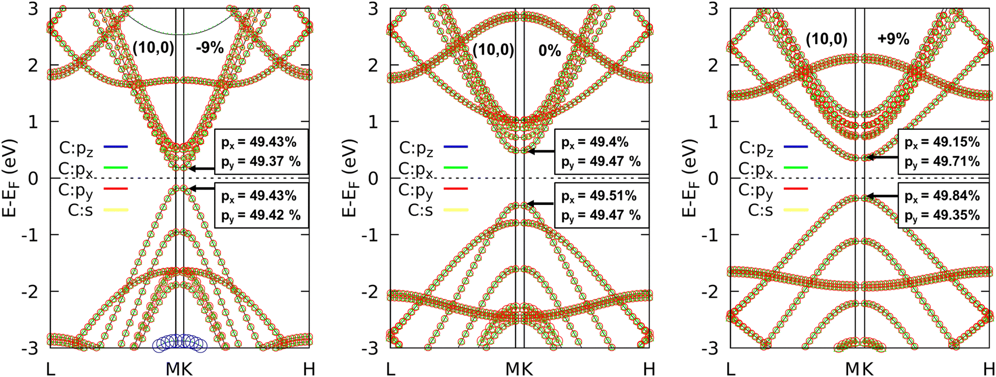 | ||
| Fig. 6 Orbital projected band structures of (10,0) SWCNT at −9%, 0% (relaxed state), and +9% uniaxial strains. | ||
3.3 Impact of strain on TE properties of SWCNTs
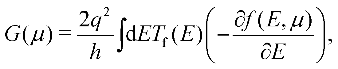
A temperature gradient ΔT applied between two junctions of dissimilar electrical conductors or semiconductors produces a potential difference ΔV between them. This is a well-known phenomenon, termed as Seebeck effect.8 The physics behind this can be described based on the principles outlined in Fermi–Dirac distribution function, a significant proportion of electron distribution occurs above the Fermi level at the hot junction, while it is small in amount at the cold junction. The charge carriers of the hot region gain kinetic energy, which makes them more agile than those at the cold region. Consequently, carriers (either electrons above the Fermi level or holes below the Fermi level) diffuse from the high temperature to low temperature junction, which creates a difference in chemical potential between the two junctions due to shifting of the Fermi levels, resulting in a potential difference between the junctions. This interesting thermoelectric property is quantified as the potential difference (ΔV) generated due to the per unit temperature change (ΔT), which is known as the Seebeck coefficient S = −ΔV/ΔT. However, to obtain the net current, thermoelectric devices are made of either p-type or n-type materials to ensure net charge flow from the hot to cold junction. Otherwise, the electrons and hole will recombine during their movements resulting in no net electronic current flow. Since CNTs can be of both p-type and n-type, a TE device with single chirality CNT is possible to make.30 The calculation of transport parameters as per eqn (2) and (3) can be performed within the framework of Boltzmann transport equation (BTE).29 We calculated the thermoelectric parameters such as S, σ, and TE PF using semiclassical Boltzmann transport theory within the constant relaxation time approximation (CRTA) using ab initio approach. The Seebeck coefficient S(μ) and electrical conductance G(μ) as a function of chemical potential μ are expressed as,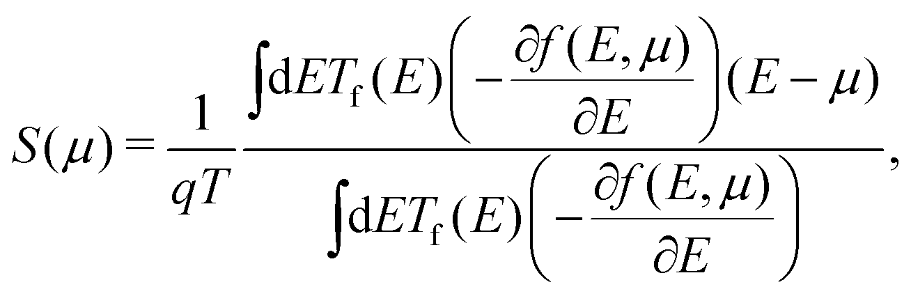 | (2) |
 | (3) |
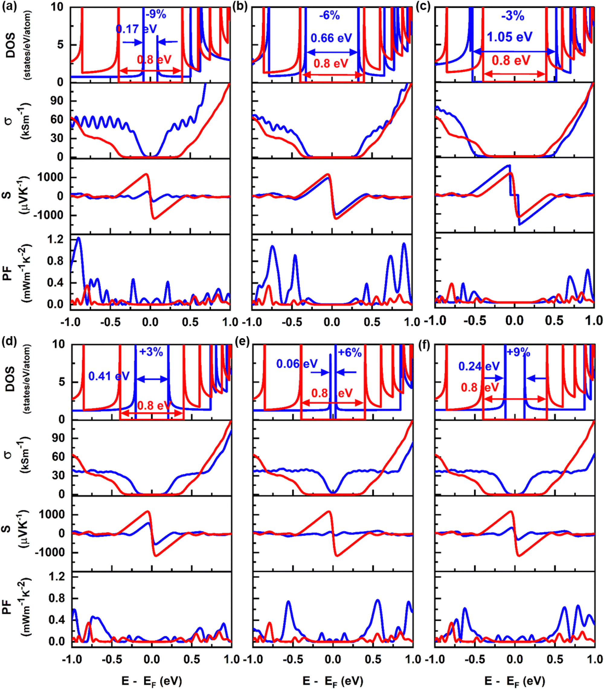 | ||
| Fig. 7 The DOS, σ, S, and PF of the (11,0) SWCNT as a function of chemical potential at (a) −9%, (b) −6%, (c) −3%, (d) +3%, (e) +6%, and (f) +9% strains. The red colored graph is for the relaxed state (0% strain). | ||
 | ||
| Fig. 8 (a) Variation of the absolute value of Seebeck coefficient with uniaxial strain for (10,0), (11,0), (9,0), and (6,6) SWCNTs. (b) The calculated Seebeck coefficient with carrier concentration at different levels of uniaxial strains for p and n-type (11,0) SWCNTs at 300 K. | ||
 , increased mobility
 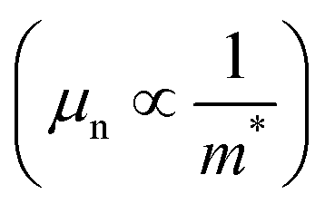 of electron transport and enhanced electrical conductivity (σ = qnμn) (see Fig. S3(a)–(c) of the ESI†). In contrast, the curvature of the bands at the CBM became broader upon applying tensile strain on (10,0) SWCNTs, causing the reduction of σ (see Fig. S3(d)–(f) of the ESI†). In (11,0) SWCNTs, σ decreased with an increment of compressive strain, the exact reverse of the trend obtained for (10,0) SWCNTs as seen in Fig. 7. Though the curvature of the CBM in the band structure of (11,0) SWCNTs was stronger with the increment of compressive strain, the depletion of energy states outside of CNP lessened σ. On the contrary, owing to the same curvature of CBM and VBM, and also the constant number of energy states in the DOS, σ remained mostly unaltered with tensile strains on (11,0) SWCNTs as can be seen in Fig. 7. For (9,0) SWCNTs, which exhibited quasi-metallic characteristics with a pseudo gap of ∼0.19 eV and outside of the first vHs, energy states were established, which can be observed in the DOS plot as portrayed in Fig. S4 of the ESI.† The number of valence band (VB) energy states (at the left of the 1st vHs) was consistent, which was verified by the steadiness of σ in that region. Conversely, there was an increased number of conduction band (CB) energy states compared with that in VB, which demonstrated the higher value of σ at the right of the 1st vHs. The σ was nearly uniform up to −6% of εz due to the constant number of electronic energy states in p-type (9,0) SWCNTs. However, further application of compressive strain (−9%) raised σ, which is evident from the DOS curve shown in Fig. S4(a) of the ESI.† On the contrary, when subjected to tensile strain, σ was unaffected in the vicinity of the outer region of the 1st vHs due to the uniform number of states. Purely metallic, armchair type (6,6) SWCNTs exhibited the highest electrical conductivity compared to its semiconducting and quasi-metallic counterparts studied in this paper, owing to the availability of energy states inside the 1st vHs and also increased number of states beyond that. No significant change was observed in electrical conductivity when applying compressive stress on (6,6) SWCNTs. However, σ dropped slightly upon applying tensile stress because of the reduced number of energy states (see Fig. S5(d)–(f) of the ESI†).
3.4 Carrier concentration dependent TE properties at different strains
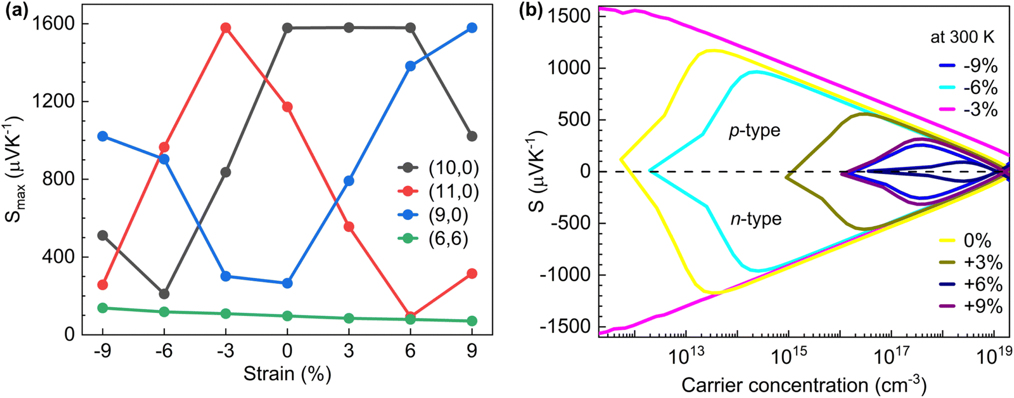
In Fig. 8(b), we present the variation of S with carrier concentrations at different strain levels at room temperature (300 K) for (11,0) SWCNTs. The peak of the absolute value of S (1172 μV K−1) occurred at ∼3.6 × 1013 cm−3 for p-type carrier concentration and at ∼3.2 × 1013 cm−3 for n-type carrier concentration without applying strain. Upon application of 3% compressive strain, S increased by 407 μV K−1 at two order of decreased carrier concentration (∼2 × 1011 cm−3) for both type of carriers. The value of S changed with the variation of the material's band gap, as tuned by applying uniaxial stress, which in turn affected S. Since the band gap of (11,0) SWCNTs was the highest at −3% strain which resulted in the highest S (1579 μV K−1), and decreased S until +6% strain. The peak point of S shifted from low to high carrier concentrations with a decrement of S. However, for a particular strain level, S reduced and diminished to zero at a concentration of ∼1019 cm−3 for both types of carriers at room temperature. On the other hand, the electrical conductivity (σ) was low at the carrier concentration <1 × 1020 cm−3 for (11,0) SWCNTs (see Fig. 9(a) and (e)). However, under relaxed conditions (without strain), with increased carrier concentrations (>1 × 1020 cm−3), the σ for n-type (11,0) SWCNTs was relatively larger than that of the p-type system, which is consistent with the DOS curve, due to the increased number of electronic energy states at the conduction bands. On the application of strain, we found a larger value of σ for n-type (11,0) SWCNTs compared with that of the p-type system above 1 × 1020 cm−3 carrier concentration. The σ increased more at compressive strains than at tensile ones. We found that the peak value of S occurred within the carrier concentration of 1011 cm−3 to 1019 cm−3, while the σ increased significantly when the carrier concentration was above 1 × 1020 cm−3. Hence, the doping level should be optimized to obtain the best thermoelectric power factor.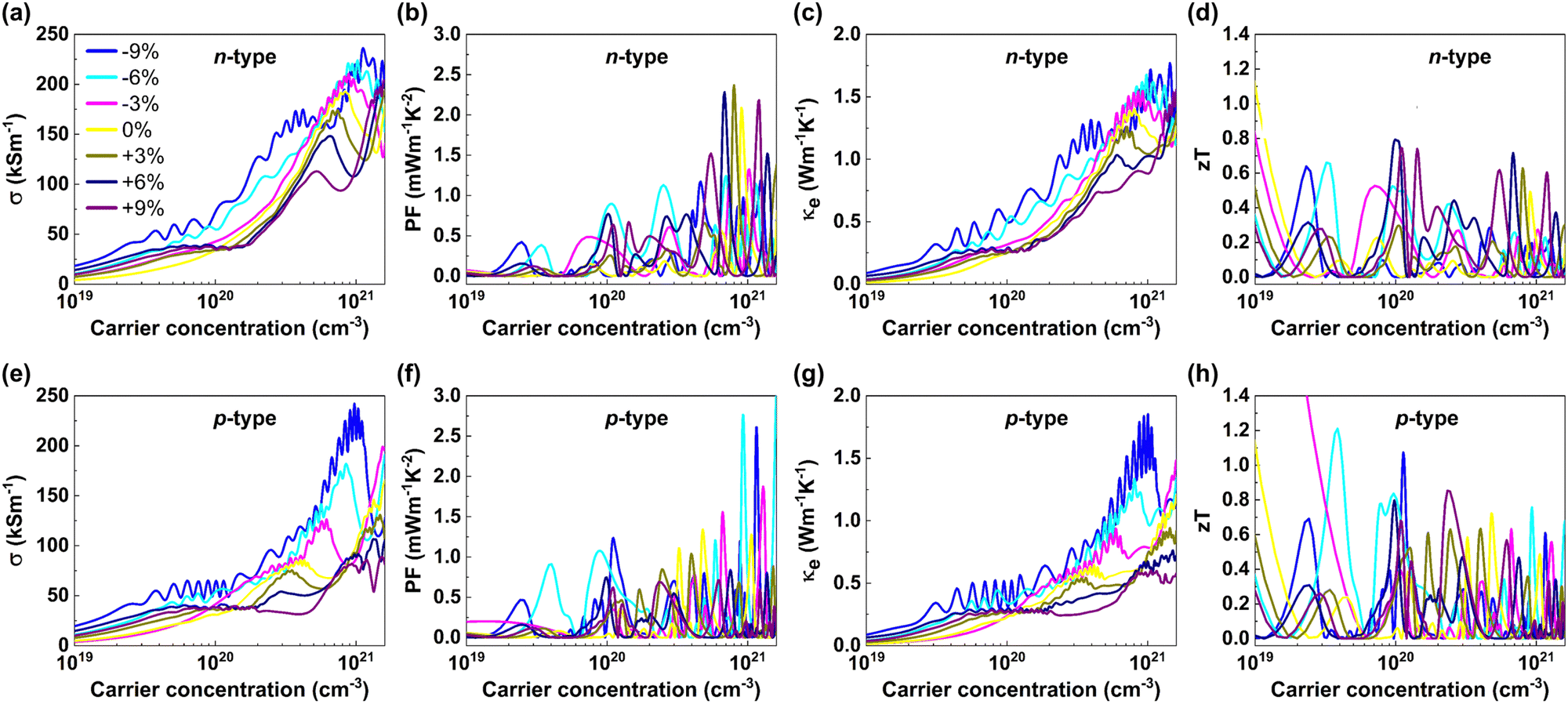 | ||
| Fig. 9 The calculated strain dependent thermoelectric transport properties as a function of carrier concentration for the (11,0) SWCNT at 300 K: (a) and (e) electrical conductivity σ, (b) and (f) power factor, (c) and (g) electron induced thermal conductivity κe, and (d) and (h) figure of merit zT for n-type and p-type carrier concentrations, respectively. | ||
The strain-dependent TE PF with respect to carrier concentration for (11,0) SWCNT is plotted in Fig. 9(b) and (f). Our calculation revealed that the p-type system for (11,0) SWCNT was dominant in terms of TE PF over the wider range of carrier concentration (1019–1021 cm−3) at each level of strain. The peak value of PF obtained without applying strain was 1.34 mW m−1 K−2 at a p-type carrier concentration of 4.8 × 1020 cm−3. However, it increased to ∼2.76 mW m−1 K−2 at −6% strain at the carrier concentration of 9.24 × 1020 cm−3 for p-type (11,0) SWCNTs, which is ∼2-fold of unstrained CNTs. On the other hand, for n-type (11,0) SWCNTs, TE PF was significantly large when it was strained. The highest PF obtained was ∼2.36 mW m−1 K−2 at +3% strain with an n-type carrier concentration of 8 × 1020 cm−3.
Another performance parameter for thermoelectric nanogenerators is thermal conductivity (κ), which has two components: one comes from electron contribution (κe), and the other is due to lattice vibration (κl). We calculated the electron-induced thermal conductivity κe in terms of carrier relaxation time constant τ. As of other transport parameters such as electrical conductivity σ and TE PF, we considered a reference value τ = 0.8 × 10¹⁴ s to analyze the impact of strain on SWCNTs qualitatively. We plotted the electron-induced thermal conductivity κe of (11,0) SWCNTs in terms of carrier concentration in Fig. 9(c) and (g) for p-type and n-type carriers. At unstrained (11,0) SWCNTs, κe remained unchanged up to 2.55 × 1020 cm−3 carrier concentration for both of the carrier types. However, above 2.55 × 1020 cm−3, κe increased significantly for n-type carriers until the carrier concentration reached 1.3 × 1021 cm−3, which indicated an enhanced performance for thermoelectric cooling using the Peltier effect. On the application of tensile stress, κe decreased for both carrier types. The value of κe was minimum at +9% strain over the whole range of carrier concentrations due to increased resistance to heat conduction upon applying tensile stress.
The overall performance of a TE device is assessed by the dimensionless parameter figure of merit zT factor (S2σTκ−1). In Fig. 9(d) and (h), we plotted the strain modulated zT with carrier concentration for (11,0) SWCNT at 300 K. At low carrier concentration, the zT factor was larger than that at a high carrier concentration, which was significantly caused due to low thermal conductivity at low carrier concentration. However, the enhancement of TE PF was obtained at around 1021 cm−3 carrier concentration for both types of carriers. At around this carrier concentration, the highest value of zT for unstrained (11,0) SWCNT was 0.72 and 0.5, occurring at 4.8 × 1020 cm−3 and 9 × 1020 cm−3 for p and n-type carrier concentrations, respectively. Upon application of uniaxial stress, zT increased significantly for both carrier types; for instance it was 1.21 at 3.86 × 1019 cm−3, which is 1.7 times that at unstrained p-type (11,0) SWCNTs and it increased to 0.8 for n-type (11,0) SWCNTs at room temperature. The peak values of thermoelectric transport parameters achieved in this study within the chemical potential range −1 eV to +1 eV at 300 K are summarized in Table 3.
| SWCNT | S max (μV K−1) | σ max (kS m−1) | PFmax (mW m−1 K−2) | κ e(min) (W m−1 K−1) | zT max | zT unstrained |
|---|---|---|---|---|---|---|
| (6,6) | 138 (−9%) | 174 (−9%) | 2.2 (−9%) | 0.11 (+9%) | 1.25 (+9%) | 0.94 |
| (9,0) | 1579 (+9%) | 118 (−6%) | 1.3 (−3%) | 0.2 (+9%) | 1.56 (−9%) | 0.71 |
| (10,0) | 1580 (+3%) | 115 (−9%) | 1.15 (−3%) | 0.13 (+6%) | 1.1 (+6%) | 0.88 |
| (11,0) | 1579 (−3%) | 120 (−9%) | 1.24 (−9%) | 0.24 (+9%) | 1.21 (−6%) | 1.07 |
As we calculated the electronic DOS with respect to energy, it is required to know the level of doping of the SWCNT system to achieve the desired chemical potential (μ). Hence, we calculated and plotted the chemical potential with carrier concentration for (11,0) SWCNTs in Fig. 10 under different levels of strains. The effect of strain on the variation of μ with carrier concentration followed a similar trend at low carrier concentration (<5.8 × 1019 cm−3) for both p and n-type (11,0) SWCNTs at room temperature.
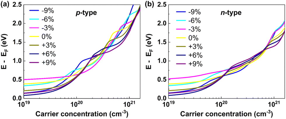 | ||
| Fig. 10 The change of chemical potential with doping level for (a) p-type and (b) n-type carriers for (11,0) SWCNTs. The Fermi level was set to 0 eV. | ||
3.5 Temperature dependent TE properties at different strains
In Fig. 11, the temperature-dependent thermoelectric transport parameters for (6,6), (9,0), (10,0), and (11,0) SWCNTs are plotted at particular carrier concentrations, where their peak performances were obtained. At low temperatures, the value of S was higher, as shown in Fig. 11(a) and (b). In contrast, S decreased with an increase in the temperature, primarily due to bipolar transport. The bipolar transport was substantially high at elevated temperatures with low carrier concentrations, since the minority carrier generation occurred due to thermal agitation. On the other hand, the number of empty states above the Fermi level is comparatively lower at high temperatures than at low temperatures. These phenomena collectively resulted in a decrease of Seebeck coefficient at high temperatures compared to that at low temperatures. However, the bipolar transport might be more pronounced at elevated temperatures and cause a significant reduction of S with even sign reversal, as observed for n-type (10,0) SWCNTs. We plotted Fig. 11(b) particularly for (10,0) SWCNTs, where the bipolar transport was more significant and sign reversal of S occurred above 550 K for a donor concentration level of 1.1 × 1011 cm−3 at the relaxed state.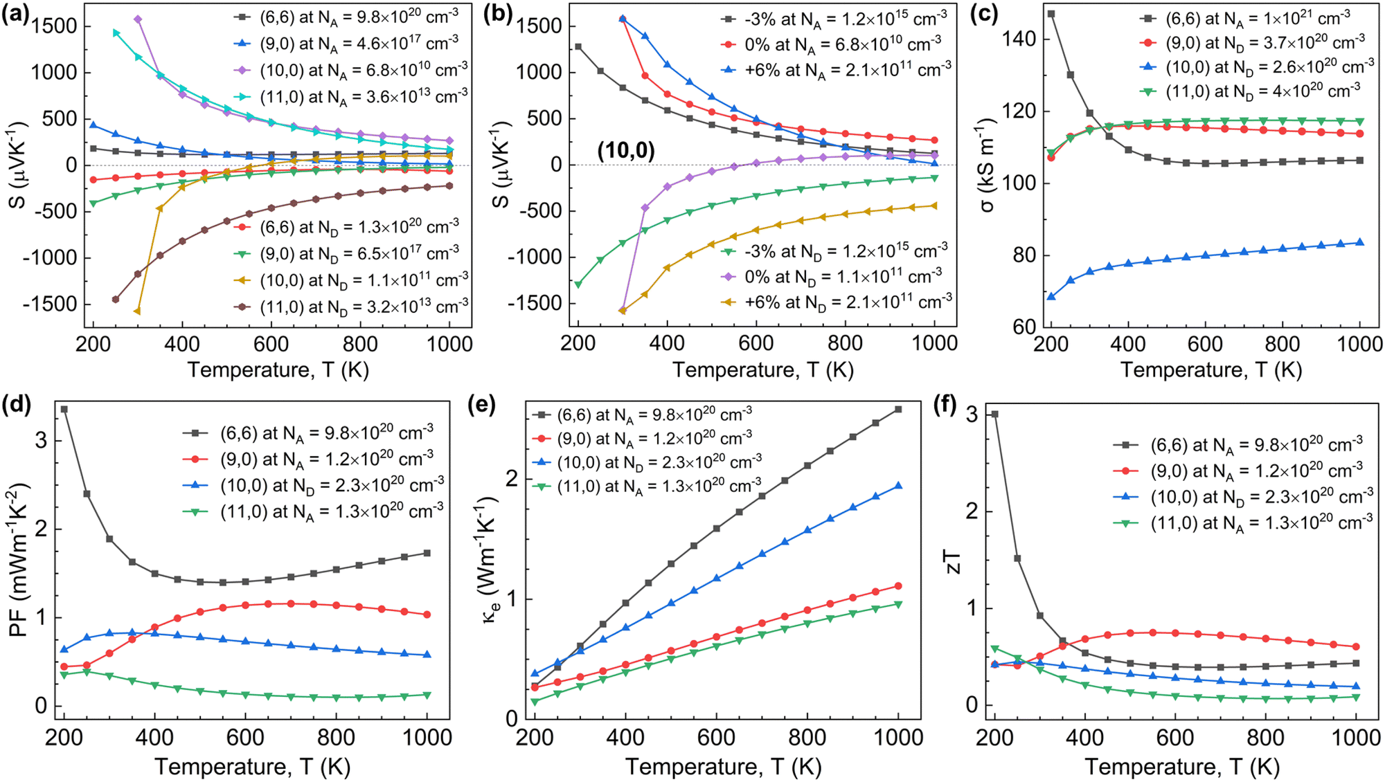 | ||
| Fig. 11 The calculated thermoelectric transport parameters as a function of temperature: (a) and (b) Seebeck coefficient (c) electrical conductivity σ, (d) thermoelectric power factor, (e) electronic thermal conductivity κe, and (f) thermoelectric figure of merit zT. | ||
The electrical conductivity σ for (6,6) SWCNTs was calculated with an acceptor (NA) doping concentration of 1 × 1021 cm−3. The σ was high at low temperatures and started to decrease with increasing the temperature. Above 500 K, it went to a steady-state value of ∼108 kS m−1 for p-type (6,6) SWCNTs. However, for (10,0) and (11,0) semiconducting SWCNTs and a quasi-metallic type (9,0) SWCNTs, the reverse trend was observed at the donor (ND) concentration of (2.6–4) × 1020 cm−3. It can be inferred that above room temperature, the σ was dominant for semiconducting SWCNTs compared with metallic SWCNTs, while the reverse was obtained below room temperature. The (9,0) and (11,0) SWCNTs revealed approximately the same value of σ and the similar trend with respect to temperature change. At elevated temperatures, the σ for (9,0), (10,0), and (11,0) SWCNTs reached to a steady-state value of approximately 118 kS m−1, 80 kS m−1, and 120 kS m−1, as can be observed in Fig. 11(c).
The Seebeck coefficient and electrical conductivity-dependent parameter thermoelectric power factor, PF, responded with a similar trend as that of σ. With increasing temperature, the PF increased for quasi-metallic (9,0) SWCNTs, while it decreased for purely metallic (6,6) SWCNTs. However, the PF increased for (10,0) SWCNTs above room temperature, while it decreased slightly for (11,0) SWCNTs. The highest PF was achieved in armchair type (6,6) metallic SWCNTs, compared to semiconducting SWCNTs at all temperatures, due to its increased electrical conductivity and decent value of S (see Fig. 11(d)).
Thermal conductivity is another key parameter to optimize the thermoelectric performance of TE devices. We calculated the SWCNTs' electronic thermal conductivity, κe at different temperatures under certain carrier concentrations, where the low value of κe was observed. The κe increased linearly with the increment of temperature, which was due to agitation of electrons at the elevated temperatures. The (9,0) and (11,0) SWCNTs exhibited a low value of κe compared to (6,6) and (10,0) SWCNTs (see Fig. 11(e)).
The overall performance of thermoelectric devices was evaluated by the dimensionless parameter figure of merit, zT. We calculated the zT for (6,6), (9,0), (10,0), and (11,0) SWCNTs at carrier concentrations close to the Fermi level, where they were maximum. The zT was not significantly impacted above a temperature of 400 K as can be observed in Fig. 11(f). In contrast, it was remarkably high for (6,6) SWCNTs below the room temperature because of low κe, high σ, and a decent value of S. However, above 400 K, purely metallic (6,6) and quasi-metallic (9,0) SWCNTs with p-type doping exhibited enhanced performance in terms of thermoelectric power factor and figure of merit.
4 Conclusions
We systematically investigated the impact of uniaxial strain on SWCNTs' electronic and thermoelectric properties, adopting first-principles calculations together with Boltzmann transport theory. A greater amount of hydrostatic pressure was required for stretching at smaller strains, while the opposite was observed for larger strains. Applying uniaxial stress, the band gap was opened for armchair SWCNTs, and the band gap of the semiconducting nanotubes was quenched. The band gap varied as a zigzag pattern with εz for all the SWCNTs. This pattern of the band gap variation with strain was obtained due to the shifting of the Dirac points and allowed k lines. The semiconductor-to-metal transition occurred in between −6% and −9% strains for the (10,0) SWCNT and at +6% for the (11,0) SWCNT. In contrast, the trend of S22 variation with strain was opposite to that in S11. The calculated DOS of the respective structure validated the electronic band gaps obtained from band structures. The Seebeck coefficients were tuned to 210–1580, 93–1579, 301–1579, and 71–138 μV K−1 for (10,0), (11,0), (9,0), and (6,6) SWCNTs, respectively. The variation of S with strain followed a similar pattern to that obtained for the band gap. The peak of S was attained at a low carrier concentration compared to other transport parameters. The absolute value of S decreased with the increase of carrier concentrations for both p and n-type carriers and diminished to zero above the concentration of ∼1 × 1019 cm−3. The electrical conductivity σ increased with compressive strains, while it lessened with tensile strains, and the change of σ was significant above ∼1 × 1020 cm−3 carrier concentration for both type of carriers. The overall thermoelectric performance parameter zT factor was enhanced by applying uniaxial stress on the SWCNTs. Our calculated results implied that the enhancement of thermoelectric performance and the tunability of TE parameters of the SWCNTs can be achieved through the application of uniaxial strain and the doping level should be optimized within 5 × 1019 cm−3–1 × 1021 cm−3 with p-type carriers to attain the optimal value of TE PF and zT factor at room temperature. However, at elevated temperatures, the S decreased and sign reversal occurred at low carrier concentration and σ increased slightly for semiconducting SWCNTs. In this study, we comprehensively analyzed the impact of uniaxial strains on the thermoelectric properties of different chirality SWCNTs and explained the physics behind their modification with strain, since the strains are very natural in multi-functional CNT fibers. Our findings can be employed in multi-functional CNT-based TEGs to improve their performance. The wide range of varying electronic properties can also be applied in flexible and wearable optoelectronic devices due to their direct band gap conservation at all strains.Author contributions
Md. Mafizul Islam: conceptualization, formal analysis, methodology, visualization, software, investigation, and writing – original draft. Ahmed Zubair: supervision, conceptualization, methodology, visualization, project administration, resources, writing – original draft, and writing – review & editing.Conflicts of interest
There are no conflicts to declare.Acknowledgements
M. M. I. and A. Z. acknowledge the support and necessary facilities provided by the Department of Electrical and Electronic Engineering, Bangladesh University of Engineering and Technology (BUET). M. M. I. and A. Z. thank Bangladesh Research and Education Network (BdREN) for providing computational facilities. A. Z. acknowledges the Basic Research Grant (Sonstha/R-60/Ref-4747) provided by BUET.References
- J. A. Rogers, Nat. Nanotechnol., 2017, 12, 839–840 CrossRef CAS PubMed.
- R. Gravina, P. Alinia, H. Ghasemzadeh and G. Fortino, Information Fusion, 2017, 35, 68–80 CrossRef.
- A. Balakrishnan, J. Medikonda, P. K. Namboothiri and M. Natarajan, Eng. Sci., 2022, 19, 5–19 Search PubMed.
- W. Huang, E. Tokunaga, Y. Nakashima and T. Fujigaya, Sci. Technol. Adv. Mater., 2019, 20, 97–104 CrossRef CAS PubMed.
- X. Jiang, Y. Chen, X. Meng, W. Cao, C. Liu, Q. Huang, N. Naik, V. Murugadoss, M. Huang and Z. Guo, Carbon, 2022, 191, 448–470 CrossRef CAS.
- Z. Lin, X. Li, H. Zhang, B. B. Xu, P. Wasnik, H. Li, M. V. Singh, Y. Ma, T. Li and Z. Guo, Inorg. Chem. Front., 2023, 10, 4358–4392 RSC.
- F. Islam, A. Zubair and N. Fairuz, 2019 IEEE Student Conference on Research and Development (SCOReD), 2019.
- N. T. Hung, A. R. T. Nugraha and R. Saito, Energies, 2019, 12, 4561 CrossRef CAS.
- CRC Handbook of Thermoelectrics, ed. D. Rowe, CRC Press, 2018 Search PubMed.
- R. Mondal, M. A. M. Hasan, R. Zhang, H. Olin and Y. Yang, Adv. Mater. Technol., 2022, 7, 2200282 CrossRef.
- C. Zeng, P. Stenier, K. Chen, K. Wan, M. Dong, S. Li, C. Kocabas, M. J. Reece, D. G. Papageorgiou, A. N. Volkov, H. Zhang and E. Bilotti, Mater. Horiz., 2023, 10(9), 3601–3609 RSC.
- Y. Zou, L. Bo and Z. Li, Fundam. Res., 2021, 1, 364–382 CrossRef CAS.
- C. Wu, A. C. Wang, W. Ding, H. Guo and Z. L. Wang, Adv. Energy Mater., 2018, 9, 1802906 CrossRef.
- J. Shao, M. Willatzen and Z. L. Wang, J. Appl. Phys., 2020, 128, 111101 CrossRef CAS.
- S. G. Pawar, N. V. Pradnyakar and J. P. Modak, J. Phys.: Conf. Ser., 2021, 1913, 012042 CrossRef CAS.
- G. Luo, Q. Zhang, M. Li, K. Chen, W. Zhou, Y. Luo, Z. Li, L. Wang, L. Zhao, K. S. Teh and Z. Jiang, Nanotechnology, 2021, 32, 405402 CrossRef CAS PubMed.
- N. Komatsu, Y. Ichinose, O. S. Dewey, L. W. Taylor, M. A. Trafford, Y. Yomogida, G. Wehmeyer, M. Pasquali, K. Yanagi and J. Kono, Nat. Commun., 2021, 12, 4931 CrossRef CAS PubMed.
- B. Poudel, Q. Hao, Y. Ma, Y. Lan, A. Minnich, B. Yu, X. Yan, D. Wang, A. Muto, D. Vashaee, X. Chen, J. Liu, M. S. Dresselhaus, G. Chen and Z. Ren, Science, 2008, 320, 634–638 CrossRef CAS PubMed.
- J. P. Heremans, V. Jovovic, E. S. Toberer, A. Saramat, K. Kurosaki, A. Charoenphakdee, S. Yamanaka and G. J. Snyder, Science, 2008, 321, 554–557 CrossRef CAS PubMed.
- L. Yang, Z.-G. Chen, M. S. Dargusch and J. Zou, Adv. Energy Mater., 2017, 8, 1701797 CrossRef.
- B. Russ, A. Glaudell, J. J. Urban, M. L. Chabinyc and R. A. Segalman, Nat. Rev. Mater., 2016, 1, 16050 CrossRef CAS.
- S. H. Lee, H. Park, S. Kim, W. Son, I. W. Cheong and J. H. Kim, J. Mater. Chem. A, 2014, 2, 7288–7294 RSC.
- G.-H. Kim, L. Shao, K. Zhang and K. P. Pipe, Nat. Mater., 2013, 12, 719–723 CrossRef CAS PubMed.
- Y. Du, J. Xu, B. Paul and P. Eklund, Appl. Mater. Today, 2018, 12, 366–388 CrossRef.
- E. M. F. Vieira, A. L. Pires, J. P. B. Silva, V. H. Magalhães, J. Grilo, F. P. Brito, M. F. Silva, A. M. Pereira and L. M. Goncalves, ACS Appl. Mater. Interfaces, 2019, 11, 38946–38954 CrossRef CAS PubMed.
- S. Nanot, N. A. Thompson, J.-H. Kim, X. Wang, W. D. Rice, E. H. Hároz, Y. Ganesan, C. L. Pint and J. Kono, Springer Handbook of Nanomaterials, Springer Berlin Heidelberg, 2013, pp. 105–146 Search PubMed.
- A. Zubair, D. Tristant, C. Nie, D. E. Tsentalovich, R. J. Headrick, M. Pasquali, J. Kono, V. Meunier, E. Flahaut, M. Monthioux, I. C. Gerber and P. Puech, Phys. Rev. Mater., 2017, 1, 064002 CrossRef.
- N. T. Hung and R. Saito, Adv. Quantum Technol., 2021, 4, 2000115 CrossRef CAS.
- G. D. Mahan and J. O. Sofo, Proc. Natl. Acad. Sci. U. S. A., 1996, 93, 7436–7439 CrossRef CAS PubMed.
- B. A. MacLeod, N. J. Stanton, I. E. Gould, D. Wesenberg, R. Ihly, Z. R. Owczarczyk, K. E. Hurst, C. S. Fewox, C. N. Folmar, K. Holman Hughes, B. L. Zink, J. L. Blackburn and A. J. Ferguson, Energy Environ. Sci., 2017, 10, 2168–2179 RSC.
- D. Tristant, A. Zubair, P. Puech, F. Neumayer, S. Moyano, R. J. Headrick, D. E. Tsentalovich, C. C. Young, I. C. Gerber, M. Pasquali, J. Kono and J. Leotin, Nanoscale, 2016, 8, 19668–19676 RSC.
- A. Zubair, X. Wang, F. Mirri, D. E. Tsentalovich, N. Fujimura, D. Suzuki, K. P. Soundarapandian, Y. Kawano, M. Pasquali and J. Kono, Phys. Rev. Mater., 2018, 2, 015201 CrossRef CAS.
- P. Xie, Y. Liu, M. Feng, M. Niu, C. Liu, N. Wu, K. Sui, R. R. Patil, D. Pan, Z. Guo and R. Fan, Adv. Compos. Hybrid Mater., 2021, 4, 173–185 CrossRef CAS.
- P. Xie, Z. Zhang, K. Liu, L. Qian, F. Dang, Y. Liu, R. Fan, X. Wang and S. Dou, Carbon, 2017, 125, 1–8 CrossRef CAS.
- Z. Tang, Q. Huang, Y. Liu, Y. Chen, B. Guo and L. Zhang, ACS Macro Lett., 2019, 8, 1575–1581 CrossRef CAS PubMed.
- R. Downes, S. Wang, D. Haldane, A. Moench and R. Liang, Adv. Eng. Mater., 2015, 17, 349–358 CrossRef CAS.
- S. Dmitrović, I. Milošević, M. Damnjanović and T. Vuković, J. Phys. Chem. C, 2015, 119, 13922–13928 CrossRef.
- J.-M. Zhang, R.-L. Liang and K.-W. Xu, Phys. B, 2010, 405, 1329–1334 CrossRef CAS.
- P. H. Jiang, H. J. Liu, D. D. Fan, L. Cheng, J. Wei, J. Zhang, J. H. Liang and J. Shi, Phys. Chem. Chem. Phys., 2015, 17, 27558–27564 RSC.
- M. M. Islam and A. Zubair, 2022 12th International Conference on Electrical and Computer Engineering (ICECE), 2022, pp. 425–428.
- D. Dass, Superlattices Microstruct., 2018, 120, 108–126 CrossRef CAS.
- J. R. Deji, M. Chauhan and R. K. Sharma, ES Energy Environ., 2022, 18, 47–55 Search PubMed.
- P. Giannozzi, S. Baroni, N. Bonini, M. Calandra, R. Car, C. Cavazzoni, D. Ceresoli, G. L. Chiarotti, M. Cococcioni, I. Dabo, A. D. Corso, S. de Gironcoli, S. Fabris, G. Fratesi, R. Gebauer, U. Gerstmann, C. Gougoussis, A. Kokalj, M. Lazzeri, L. Martin-Samos, N. Marzari, F. Mauri, R. Mazzarello, S. Paolini, A. Pasquarello, L. Paulatto, C. Sbraccia, S. Scandolo, G. Sclauzero, A. P. Seitsonen, A. Smogunov, P. Umari and R. M. Wentzcovitch, J. Phys.: Condens. Matter, 2009, 21, 395502 CrossRef PubMed.
- G. K. Madsen and D. J. Singh, Comput. Phys. Commun., 2006, 175, 67–71 CrossRef CAS.
- A. M. Ganose, J. Park, A. Faghaninia, R. Woods-Robinson, K. A. Persson and A. Jain, Nat. Commun., 2021, 12, 2222 CrossRef CAS PubMed.
- N. W. Ashcroft and N. D. Mermin, Solid State Physics, Cengage Learning, 1976 Search PubMed.
- K. Kato, T. Koretsune and S. Saito, Phys. Rev. B: Condens. Matter Mater. Phys., 2012, 85, 115448 CrossRef.
- M. K. Niranjan, J. Phys. Commun., 2020, 4, 015004 CrossRef CAS.
- K.-M. Lin, Y.-H. Huang, W. Su and T. Leung, Comput. Phys. Commun., 2014, 185, 1422–1428 CrossRef CAS.
- G. Sun, J. Kürti, M. Kertesz and R. H. Baughman, J. Phys. Chem. B, 2003, 107, 6924–6931 CrossRef CAS.
- M. Ouyang, J.-L. Huang, C. L. Cheung and C. M. Lieber, Science, 2001, 292, 702–705 CrossRef CAS PubMed.
- L. Yang and J. Han, Phys. Rev. Lett., 2000, 85, 154–157 CrossRef CAS PubMed.
- S. Sreekala, X.-H. Peng, P. M. Ajayan and S. K. Nayak, Phys. Rev. B: Condens. Matter Mater. Phys., 2008, 77, 155434 CrossRef.
- E. D. Minot, Y. Yaish, V. Sazonova, J.-Y. Park, M. Brink and P. L. McEuen, Phys. Rev. Lett., 2003, 90, 156401 CrossRef CAS PubMed.
- Y. Zhang and M. Han, Phys. E, 2011, 43, 1774–1778 CrossRef CAS.
Footnote |
| † Electronic supplementary information (ESI) available. See DOI: https://doi.org/10.1039/d3ma00713h |
| This journal is © The Royal Society of Chemistry 2023 |