
 Open Access Article
 This Open Access Article is licensed under a Creative Commons Attribution-Non Commercial 3.0 Unported Licence
Experimental design of stencil-printed high-performance organic electrochemical transistors†
Amir Mohammad
Ghafari
a,
Michele
Catacchio
b,
Emil
Rosqvist
 c,
Axel
Luukkonen
a,
Anni
Eklund
a,
Kim
Björkström
a,
Paolo
Bollella
de,
Luisa
Torsi
ade,
Eleonora
Macchia
*abd and
Ronald
Österbacka
*a
c,
Axel
Luukkonen
a,
Anni
Eklund
a,
Kim
Björkström
a,
Paolo
Bollella
de,
Luisa
Torsi
ade,
Eleonora
Macchia
*abd and
Ronald
Österbacka
*a
aPhysics and Center for Functional Materials, Faculty of Science and Engineering, Åbo Akademi University, Turku, 20500, Finland. E-mail: eleonora.macchia@uniba.it; ronald.osterbacka@abo.fi
bDipartimento di Farmacia-Scienze del Farmaco, Università degli Studi di Bari “Aldo Moro”, Bari, 70125, Italy
cPhysical Chemistry, Laboratory of Molecular Science and Engineering, Åbo Akademi University, Turku, 20500, Finland
dCSGI (Centre for Colloid and Surface Science), Bari, 70125, Italy
eDipartimento di Chimica, Università degli Studi di Bari “Aldo Moro”, Bari, 70125, Italy
First published on 4th December 2023
Abstract
Organic electrochemical transistors (OECTs) are widely employed in several bioelectronic applications such as biosensors, logic circuits, and neuromorphic engineering, providing a seamless link between the realm of biology and electronics. More specifically, OECTs are endowed with remarkable signal amplification, the ability to operate in an aqueous environment, and the effective transduction of ionic to electrical signals. One main limiting factor preventing OECTs’ wide use is the need for microfabrication processes, typically requiring specialized equipment. From this perspective, a robust and cost-effective production protocol to achieve high-performing OECT would be desirable. Herein, a straightforward stencil-printed OECT fabrication procedure is proposed, where the electrical performance can be controlled by adjusting the electronic channel fabrication conditions. An experimental design approach is undertaken to optimize OECT figures of merit by varying key parameters such as the annealing temperature and time, as well as the transistor active channel length. The resulting OECT devices, fabricated through a high-yield, cost-effective, and fast stencil printing technique, feature large transconductance values at low operating voltages. The experimental design allowed for minimizing the threshold voltage (VT = 260 mV) while keeping a high on/off ratio (7 × 10³). A signal-to-noise ratio as high as 40 dB was obtained, which is among the highest for OECTs, operating in an aqueous electrolyte operated in a DC mode. An atomic force microscopy (AFM) characterization has been undertaken to analyze the channel morphology in the OECTs, correlating the annealing conditions with the charge transport properties.
1. Introduction
Organic electrochemical transistors (OECTs) have gained significant attention in bioelectronics for their ability to provide a smooth interface between biology and electronics. Based on the ionic permeability of the electronic channel materials, organic field effect transistors (OFET) working in an electrolyte can be classified into two main categories.1 Typically, EG-OFET comprises an ion-impermeable channel material, such as poly(3-hexylthiophene) (P3HT). In this case, 2D capacitances, at the gate/electrolyte interface and at the electrolyte/organic semiconductor interface are installed. At steady-state (quasi-static operation), nearly all the applied gate potential is dropped across those two interfaces and there is little potential drop in the bulk of the electrolyte. Therefore, the ionic current from the gate to source electrodes is near zero ideally (rigorously, this will never be the case due to impurities, for example).2 On the other hand, when the channel material is ion-permeable, the bioelectronic device is commonly addressed as OECT. In the OECT structure, the electrolyte/organic semiconductor capacitance extends into the bulk of the channel resulting in a 3D capacitance. Consequently, the operation mechanism of OECTs proceeds by the reversible electrochemical doping and de-doping (reversible oxidation or reduction, i.e., faradaic processes) of the semiconductor channel upon application and removal of a gate bias, respectively.3,4 Thus, in OECT-based devices the semiconductor channel is three-dimensional because of ion penetration and associated electrochemical doping; this in turn means that drive currents in OECTs can be enormous (the channel is thicker), which may be an advantage in specific high current applications. In particular, OECTs can efficiently transduce ionic to electronic signals and operate in aqueous environments with remarkable signal amplification, making them attractive also in biosensing applications.5–8 Those features make OECTs also suitable for implantable devices that interface with living tissues, thus making them a highly sought-after technology in health care.9,10Poly(3,4-ethylenedioxythiophene) doped with poly(styrene sulfonate) (PEDOT:PSS) is a commonly used p-channel material for OECT development, being particularly robust and stable in an aqueous solution.11 Applying a positive voltage to the gate electrode of a PEDOT:PSS-based OECT results in the injection of cations into the channel volume. This injection causes de-doping (reduction) of the PEDOT+:PSS−, subsequently reducing its electronic conductivity. Conversely, applying a negative potential to the gate electrode removes cations from the channel, resulting in the doping (oxidation) of PEDOT:PSS and a corresponding increase in its electronic (hole) conductivity. Since the subsequent source–drain current is proportional to the number of mobile holes in the channel, it can be used to determine the doping level of the organic semiconductor channel.7,9,12,13
Several OECT fabrication methods have been investigated,14,15 particularly for enhancing electrical performance and understanding the OECT-device physics.16–20 This includes developing novel organic semiconducting materials21–23 and optimizing device geometry.11,24–26 These efforts led to better-performing OECTs with faster response times, larger dynamic range, increased stability in an aqueous environment, and decreased power consumption.27 However, one of the primary constraints of OECTs is attributed to their fabrication process, typically requiring clean rooms and the use of specialized equipment to achieve optimal electronic performance levels. Although photolithography and printing methods are high-throughput and robust manufacturing processes for highly performing OECT devices, their cost remains a significant obstacle.28 Moreover, the ink formulation and the alignment of multilayer patterns pose considerable challenges.29 Despite attempts to develop simpler and cost-effective fabrication methods,30 the performance levels of OECTs fabricated through conventional microelectronic processing technologies still remain unmet. For instance, PEDOT:PSS deposition through drop-casting leads to poorly controlled channel thickness, resulting in a limited dynamic range.30,31 Moreover, screen printing is one of the commonly used techniques where patterns are created by pressing ink through a screen mask using a doctor blade. It can be adapted for roll-to-roll processes, making it suitable for large-area production. Screen printing is compatible with several organic inks and can be performed under ambient conditions. However, it requires high viscosity inks and low volatility solvents, which may limit its resolution and control over film thickness and morphology.32,33 The gravure printing technique involves engraving patterns on a rotating metallic cylinder, and ink is transferred from the cylinder wells to the substrate using a doctor blade. While it offers high-speed capabilities for large-area production, it is not suitable for printing on rigid substrates due to the required conformity between the cylinder and the substrate. Inkjet printing deposition is a promising tool for mass production, known for its relatively high production speed, low cost, selective patterning, and contactless printing capability. It also allows the use of small volumes of ink, enabling the creation of fine structures. However, the resolution of inkjet printing is influenced by ink viscosity, nozzle diameter, wetting, and binding with the substrate.34 In contrast, stencil printing offers a simpler and more cost-effective alternative to the aforementioned techniques. It involves using an open mask made from plastic adhesives to directly apply ink onto the substrate. Stencil printing is particularly cost-effective for immobilizing conductive inks on various substrates and is among the fastest techniques with a high degree of repeatability. Stencil printing's versatility also extends to both rigid and flexible substrates, making it suitable for a wide range of device designs and applications. This capability enhances the potential utility of stencil printing in various electronic and optoelectronic devices, including OECTs.35 However, one drawback is the relatively higher waste generation due to less precise control of ink application compared to screen printing.
In an ideal scenario, the dynamic operating range for PEDOT:PSS-based OECTs should span across a voltage window where all the materials involved in the device, i.e., organic semiconductor and electrodes, are redox inert.17,36 In this regard, optimizing the OECTs voltage operating window was accomplished by refining the nanoscale morphology and structure of channel materials.28 PEDOT:PSS solution has been subjected to various additives to improve the stability and adhesion of the film to the substrate,37 as well as its conductivity.38,39 For instance, incorporating organic compounds such as ethylene glycol or dimethyl sulfoxide, ionic liquids, or surfactants during processing, and post-deposition treatments with acids, have been used to enhance the electrical properties of the film.40 PEDOT:PSS, with a few commonly reported additives used, such as 4-dodecylbenzenesulfonic acid (DBSA) and ethylene glycol (EG) for conductivity and film stability, and (3-glycidyloxypropyl)trimethoxysilane (GOPS) for adhesion of the channel to the substrate and better film formation, is the most used channel material in OECTs. These combinations have been widely reported in the literature, with differences primarily related to OECT geometry or film fabrication and processing. Notably, processing temperature and time have been found to vary considerably, ranging from 50 °C to 150 °C and 5 to 120 minutes, respectively. Understanding how these variables impact electrical performance and film morphology would be extremely beneficial. Remarkably, the elicited studies typically focus on transconductance, on/off ratio, and switching speed as metrics for device performance. In addition to these parameters, the transistor's threshold voltage (VT), namely the voltage at which the transistor switches on e.g., the electrochemical potential of the gate electrode, is critical in the design of circuitry as it dictates the noise margin of digital logic and the power consumption of circuits.41 Despite its importance for OECTs, relatively little attention has been paid to controlling their threshold voltage, to the OECT operation with minimal power consumption while shifting the operating range near zero gate voltages to improve their stability.27,42
This study proposes a novel, cost-effective stencil printing fabrication method to develop high-performance OECTs.35 This technique uses an adhesive vinyl mask, combined with the stencil printing approach, to control the organic semiconductor geometry, namely the stencil length (active channel length) and active channel volume. Such a method offers many advantages being cost-effective, easily scalable to mass production, fast, and not requiring micro-electronics lab facilities. Contrary to traditional printing techniques, which are strongly affected by substrate surface energy and surface tension of the ink,43,44 stencil printing does not require particular optimization of the active material ink formulation. Remarkably, the electrical performance of the OECTs has been tuned by controlling the channel fabrication process through an experimental design approach. OECT devices were fabricated under the conditions specified by a full factorial experimental design, encompassing three variables: the annealing time, temperature, and active channel length. The OECT fabricated in the experimental condition settled by the experimental design was then electrically characterized. The on/off ratio, transconductance, and VT of the OECTs were taken as the response of the experimental design and used to determine the condition that yields the lowest operating voltage while maintaining the best electrical performance. The threshold voltage optimization has been herein performed taking into account a further application of the OECT devices as immunosensors operated in potentiometric regimes. In this case, the OECT gate electrode can be biomodified with a selected biorecognition element capable of selectively binding the affinity antigen to be assayed. In this scenario, the biofunctionalization of the gate electrode produces a decrease in the gate work function, which reflects a shift of the threshold voltage VT towards more negative potentials.45,46 This trend is replicated as the analyte standard solutions with increased concentrations are progressively assayed until the saturation of the response is reached.7 Therefore, the OECT-based devices operated as a potentiometric sensor, upon affinity binding show changes in the ID channel current, along VT shifts towards more cathodic values. Relevantly, while working with potentiometric sensors no electronic-faradaic current should flow either; hence the operational gating potentials should span across ranges where all the materials involved in the device (semiconductor, electrodes, membrane biological recognition elements, etc.) are redox inert. Therefore, the OECT operational gating window was optimized in this study bearing those constraints in mind for further operation of the OECT device as ultrasensitive potentiometric sensors. Lastly, the morphology of the OECTs fabricated according to the experimental plan was characterized with atomic force microscopy (AFM). The morphological results and the electrical characterizations provided the rationale to correlate the annealing conditions to the microstructure of PEDOT:PSS.
2. Experimental
2.1. Materials
PEDOT:PSS (PH 1000) was purchased from Ossila. (3-Glycidyloxypropyl)trimethoxysilane (98%) (GOPS), 4-dodecylbenzenesulfonic acid (DBSA), and ethylene glycol (1,2-ethanediol) were purchased from Sigma Aldrich. Sodium chloride (NaCl) was purchased from VWR Chemicals. 2-Propanol (IPA) was purchased from Merck. Cricut Smart Vinyl Removable sheet 33 × 91 cm (black) was purchased from Cricut.2.2. OECT setup fabrication
The fabrication of organic electrochemical transistors (OECTs) on glass substrates required multiple steps, as shown in Fig. 1(a)–(d).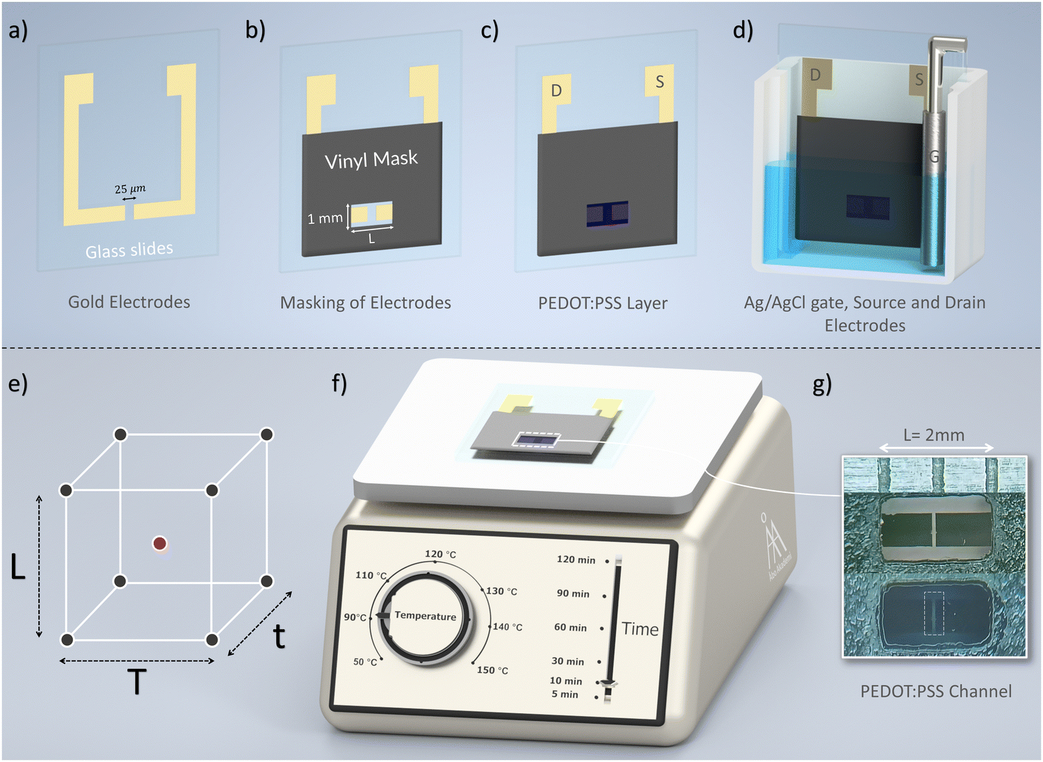 | ||
| Fig. 1 Schematic illustration of fabrication and optimization of organic electrochemical devices. The fabrication process is depicted step-by-step, with (a) gold evaporation on glass using the shadow masking technique. The width of the wire affixed to the mask determines the gap between the source–drain electrodes. In (b) the gold electrodes are cleaned, and a vinyl adhesive mask is applied to define the PEDOT:PSS region. Subsequently, in (c) the PEDOT solution is deposited, and the annealing procedure is performed. In the setup (d) the glass slide is inserted into a slide container, and the Ag/AgCl wire is the gate of the OECT. The electrolyte used in this setup is 0.1 M NaCl. (e) A visual representation of a 23 factorial design is shown, (L) represents active channel length, (T) as the temperature, and (t) as the time, and (f) shows the range of time and temperature of OECTs reported in the literature, as depicted on the hotplate adjustment menus. In (g) an optical image of a L = 2 mm device with and without the PEDOT:PSS. | ||
The glass substrate was rinsed with deionized water and then sonicated for 10 minutes in 2-propanol (IPA) to remove contaminants. As shown in Fig. 1(a), the source and drain electrodes were fabricated by evaporating titanium and gold onto a glass substrate using the shadow masking technique, with a thin wire (25 μm) attached to the shadow mask to define the channel area (the gap between the electrodes). The titanium layer was 10 nm thick, and the gold layer was 50 nm. Next, a vinyl adhesive sheet was cut using a laser cutter to delineate the area for depositing the PEDOT:PSS layer. As illustrated in Fig. 1(b), the mask serving for the stencil printing had a width of 1 mm and a length of L, which was prepared in three different sizes: 1.5 mm, 2 mm, and 2.5 mm. The PEDOT:PSS solution was made by mixing 1% GOPS, 1% ethylene glycol, 0.25% DBSA, and 98.75% PEDOT:PSS by volume. The solution was stirred for one hour. Then, as shown in Fig. 1(c), the PEDOT:PSS solution was deposited on the desired area of the gold electrodes, masked by the stencil. The ability to create a custom mask on a Smart Vinyl adhesive sheet using a Cricut Explore® 3 machine and Design Space Software v.7.3.95 allows for easy customization and precise control over the shape and dimensions of the printed PEDOT:PSS channel. The thickness of the PEDOT:PSS film was kept fixed at 90–100 μm, being defined by the thickness of the Smart Vinyl adhesive mask used for the organic semiconductor stencil printing. Indeed, the thickness of the adhesive mask is limited by the low viscosity of the PEDOT:PSS ink. Indeed, using a higher thickness of the adhesive mask would result in a non-homogeneous film, thus affecting the devices’ electronic performance levels. To increase the adhesive mask thickness and control the printing resolution, it would be preferable to use other printing techniques, such as 3D printing. Thus, this would require the use of a more complex fabrication apparatus along with additional ink optimization.47 The devices were annealed at various temperatures (90 °C as the lowest to 140 °C as the highest) and times (10 minutes and 120 minutes), in accordance with the experimental design, sketched in Fig. 1(e) (vide infra). All devices were prepared and freshly electrically characterized. Following the deposition of the PEDOT:PSS layer, the gold electrodes in contact with the electrolyte were isolated using dielectric ink. The devices were cleaned and placed in a sample holder filled with 8 mL of NaCl solution (0.1 M) as the electrolyte, as shown in Fig. 1(d). An Ag/AgCl lab-made wire served as the gate electrode. A two-electrode chronopotentiometry setup was used to prepare the wire, with a platinum coil as the counter electrode and a silver wire as the working electrode. The Ag/AgCl electrode was fabricated by applying a constant current of 0.1 mA for four hours in a 0.1 M NaCl solution. In the final step, the Ag/AgCl electrode was placed in the sample holder hosting the OECT device, and the electrolyte solution and the electrical characterizations were conducted. Remarkably, as part of future perspective, an alternative approach encompassing stencil printing of source and drain electrodes could be cosuderend using gold nanoparticle-based ink. This could potentially lead to a reduction in device production costs. Notably, a recent study has demonstrated the successful fabrication of stencil-printed electrodes using water-based graphite inks.35
2.3 Electrical characterization of the OECT
All the OECT devices were characterized using an Agilent Technologies 4142B semiconductor characterization system in air at room temperature (20 °C) in a dark box. The transfer characteristics were measured by acquiring the drain current (ID) while scanning the gate voltage (VG) in the range −0.6 to 0.9 V, at a drain voltage (VD) equal to −0.4 V. The voltage step was 1 mV. The source is grounded as typical for common source configuration measurements. The potential window was defined to prevent any electrochemical processes, which were monitored by recording the gate current (IG). The on/off ratio for each device was evaluated as the ratio between the ID registered at VG = −0.6 V and the ID at VG = 0.9 V. The OECTs source–drain current ID current measured are of the orders of mA, with a resolution of 1 nA. The transconductance, defined as (gm), was evaluated as .13 The transconductance usually is regarded as the key figure of merit of OECTs. The threshold voltage (VT) is the gate voltage at which the conduction channel starts to form.48 The latter was evaluated as the intercept to the VG abscissa of the following equation, correlating the square root of the drain current as a function of the gate bias in the saturation regime.49,50
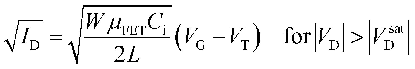 | (1) |
2.4 Experimental design
A replicated, three-factors full factorial design was developed to optimize the stencil-printed OECT fabrication (Fig. 1(e)). The factors examined were the PEDOT:PSS active channel length (L), the annealing temperature (T), and the annealing time (t) coded with X1, X2, and X3 variables, respectively. Following a two-level design, these variables were set at a low and high level, coded as −1 and +1, corresponding to the original values of 1.5 mm and 2.5 mm for L, 90 °C and 140 °C for T, and 10 minutes and 120 minutes for t. Those low and high levels were settled to explore the typical range of experimental conditions for high-performance OECT fabrication.6,51 The resulting experimental matrix is provided in Table 1. The on/off ratio, the transconductance, and the threshold voltage of the stencil printed OECT device, fabricated according to the experimental plan,46,52 were used to respond to the 23 full factorial design. The responses for each condition of the experimental plan were assessed in random order and in duplicate, leaving eight degrees of freedom available to estimate the significance of each coefficient of the model.53 In addition, the responses at the center point, encompassing a 2 mm active channel length, annealed at 115 °C for 65 minutes were evaluated in duplicate and used to validate the linear model with interactions provided by the factorial design. The model was computed as multilinear regression using CAT (Chemometric Agile Tool) open-source software.54 Statistical significance was set as customary at a confidence level p = 0.05. Indeed, each coefficient of the model is provided with a confidence interval, computed as (t·σ)/√N, where t is the critical t-student value with a confidence level of 0.05 and 8 degrees of freedom, σ is the experimental pooled standard deviation for each response, and N is the number of replicates that have been performed.| X 1 | X 2 | X 3 | L (mm) | T (°C) | t (min) | On/off ratio | g m (mS) | V T (V) |
|---|---|---|---|---|---|---|---|---|
| −1 | −1 | −1 | 1.5 | 90 | 10 | 9296 | 22.27 | 0.35 |
| −1 | −1 | −1 | 1.5 | 90 | 10 | 12093 | 25.63 | 0.34 |
| 1 | −1 | −1 | 2.5 | 90 | 10 | 7607 | 28.86 | 0.38 |
| 1 | −1 | −1 | 2.5 | 90 | 10 | 8503 | 29.41 | 0.37 |
| −1 | 1 | −1 | 1.5 | 140 | 10 | 3188 | 28.99 | 0.62 |
| −1 | 1 | −1 | 1.5 | 140 | 10 | 2498 | 30.67 | 0.63 |
| 1 | 1 | −1 | 2.5 | 140 | 10 | 3364 | 34.45 | 0.65 |
| 1 | 1 | −1 | 2.5 | 140 | 10 | 5562 | 22.69 | 0.48 |
| −1 | −1 | 1 | 1.5 | 90 | 120 | 6139 | 26.47 | 0.45 |
| −1 | −1 | 1 | 1.5 | 90 | 120 | 7570 | 32.77 | 0.48 |
| 1 | −1 | 1 | 2.5 | 90 | 120 | 5429 | 26.89 | 0.45 |
| 1 | −1 | 1 | 2.5 | 90 | 120 | 5837 | 26.89 | 0.47 |
| −1 | 1 | 1 | 1.5 | 140 | 120 | 1444 | 27.73 | 0.62 |
| −1 | 1 | 1 | 1.5 | 140 | 120 | 1104 | 21.85 | 0.69 |
| 1 | 1 | 1 | 2.5 | 140 | 120 | 2790 | 30.67 | 0.57 |
| 1 | 1 | 1 | 2.5 | 140 | 120 | 1153 | 23.11 | 0.51 |
2.5 Morphological characterizations of PEDOT:PSS
The surface topography of the samples was measured with a Bruker (US) Multimode 8 atomic force microscope (AFM) operated in PeakForce™ mode. The used silica cantilevers, ACLA by AppNano (US), had a nominal spring constant of 58 N m−1 and a radius of curvature of 6 nm, as reported by the manufacturer. Images of 5 μm × 5 μm with a resolution of 512 × 512 pixels were taken and analyzed for roughness. Imaging was done at T = 21 ± 1 °C and RH% = 23 ± 2. Image analysis was done with MountainsSPIP v.9.3.10249 (Digitalsurf, France).3. Results and discussion
In this study, OECTs are fabricated using the stencil printing concept shown in Fig. 1. The channel material is PEDOT:PSS mixture deposited on top of the gold electrodes and annealed according to the experimental design conditions in Table 1. The channel material must exhibit good charge transport properties, such as high electrical conductivity and carrier mobility, to enable the desired current flow through the device. Therefore, three different stencil sizes are applied on the electrodes, allowing for higher volumetric capacitance and lower resistance in the entire 3D channel region, improving transistor performance. The amount of channel material deposited in these devices was measured to 2 μl, to ensure a constant volume of PEDOT:PSS. The latter should be kept constant to prevent the introduction of PEDOT:PSS parasitic capacitances, leading to undesired charging and discharging of the OECT. Those parasitic capacitances might result in degrading the performance of the OECTs over time.55Fig. 2 presents the electrical characteristics of 4 devices encompassing L = 1.5 mm in size. The annealing conditions are what set these devices apart from one another. The lowest L size was chosen because it provides the maximum on/off ratio (Table 1). From the analysis of the transfer curves of the OECTs reported in Fig. 2(a), it is apparent that devices exposed to longer annealing times and higher temperatures exhibit higher currents than those exposed to shorter annealing times and lower temperatures. Indeed, these factors mainly affect the volumetric capacitance and the channel resistance. In other words, increasing the annealing temperature may increase the conductivity of the channel.
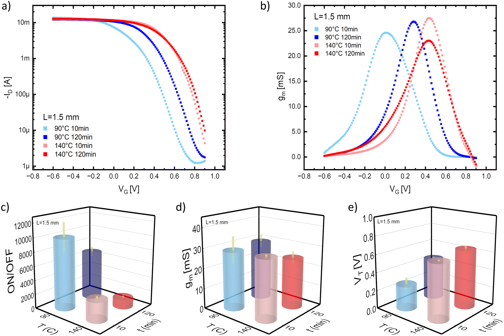 | ||
| Fig. 2 Performance of OECTs with stencil size of L = 1.5 mm under varying annealing conditions. (A) Transfer curves of devices annealed at 90 °C (blue) and 140 °C (red) for 10 minutes (light) and 120 minutes (dark), VD = −0.4 V. (b) Transconductance of devices, (c) on/off ratio with error bars (yellow lines), (d) Maximum transconductance, and (e) Threshold voltage, demonstrating the effect of temperature and time on the electrical properties of OECTs. | ||
On the other hand, decreasing the annealing temperature strongly affect the ion permeability. Therefore, higher gate voltages are needed to switch off the device. Devices fabricated at 90 °C for 10 and 120 minutes display off-state behavior at 0.8 V, which is not observed in devices fabricated at 140 °C. Moreover, as the annealing temperature and time were reduced, the transconductance peaks moved from positive to negative gate voltages. The peak occurs around zero volts at 90 °C and 10 minutes, but an additional 0.4 V is required at higher temperatures and longer times to observe the peak, as illustrated in Fig. 2(b). The on/off ratio was defined at gate voltages of −0.6 V for the on current and 0.9 V for the off current. Table 1 shows a report of these data, and Fig. 2(c) displays a selection of those results. The maximum on/off ratio has been registered for OECTs annealed at lower T and t; for those devices, the off state was accomplished at lower gate voltages. Under those experimental conditions, the organic semiconducting channel's residual water content lowers the OECT conductivity but promotes permeability and mobility during the device operation.
Moreover, the variations registered in the devices' transconductance are negligible due to our use of a thick channel and analogous geometries. Transconductance values for these devices are above 20 mS, comparable with those of OECT devices fabricated with standard microelectronic processing.8,56 In Fig. 2(e), the threshold voltage VT of the devices is plotted for each experimental condition. It can be seen that VT significantly increases with increasing annealing temperature and time processing conditions. VT represents the gate voltage at which conduction starts in the device, thus representing a transition between the on and off states. It is self-evident that increased time and temperature conditions always result in a larger value for VT due to the higher conductivity and channel structure in these settings.
Optimizing the stencil-printed OECT device has been accomplished through an experimental design approach, aiming to achieve a tunable and high-performance OECT device, i.e., maximizing the on/off ratio and the transconductance while minimizing the VT.57 To this aim, the variables engaged in the stencil printing of the OECT devices, namely the PEDOT:PSS active channel length (L), the annealing temperature (T), and time (t), have been varied according to a 23 full factorial design.53,58 In this design, each quantitative variable has two levels, coded as −1 and +1 (vide supra). The relevant experimental matrix (Table 1) encompasses eight rows (23, each row corresponding to an experiment performed in duplicate) and three columns (each column corresponding to a variable). From a geometrical point of view, as reported in Fig. 1(a), the factorial design explores the corners of a cube, thus changing contemporarily the values of all variables engaged in the design. While the experimental matrix is built up from the coded values, the experimental plan reports the real value of the variables used to evaluate the OECT performances. Thus, the OECT devices were fabricated according to the conditions settled by the experimental plan and fully electrically characterized, recording the responses, namely the on/off ratio, the threshold voltage, and the transconductance. The experiments have been performed in duplicate and random order to avoid introducing unwanted systematic effects. Based on those experiments, the following models for the on/off ratio and the threshold voltage have been obtained:
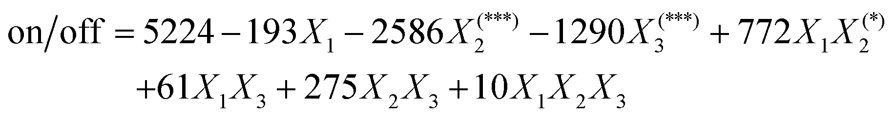 | (2) |
 | (3) |
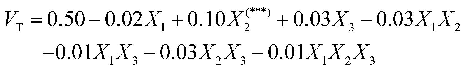
Since eight coefficients, namely a constant term, the three linear terms, the three two-term interactions, and the three-term interaction have been estimated with 16 experiments, 8 degrees of freedom were available to define the statistical significance of the coefficients. The coefficients of the on/off ratio and VT models are reported in Fig. 3(a) and (b) as bar plots. The coefficients’ significance level is indicated according to the usual convention, with *p < 0.05, **p < 0.01 and ***p < 0.001. The maximum leverage achieved for both designs is as low as 0.43. Importantly, the leverage, multiplied by the experimental variance, corresponds to the variance of the estimated response at that point.53 Thus, leverage lower than one means the response can be predicted with better precision than the experimental data collected under the same conditions. Consequently, it is possible to infer that the models hold an excellent predictive ability, i.e., leverage <1 in the whole experimental domain.
 | ||
| Fig. 3 Bar plot of the coefficients of the models of the three responses, namely (a) on/off ratio, (b) threshold voltage VT (c) transconductance gm of the 23 full factorial design. The error bars correspond to the confidence intervals at p = 0.05; the stars indicate the significance of the coefficient (* = p < 0.05, ** = p < 0.01, *** = p < 0.001). Isoresponse contour plot of (d) the on/off ratio and (e) VT. The responses registered at each annealing temperature and time are reported for a stencil length of 2 mm. For each of them, the region of acceptability is highlighted in green. (f) Multicriteria decision-making based on Pareto-front analysis for the on/off ratio and VT. The table in the insight shows the experimental condition allowing to maximize the on/off ratio while minimizing the VT. | ||
The first response is related to the on/off ratio, whose coefficients are reported in Fig. 3(a), which shall be maximized. The linear term of X2 shows an absolute value larger than the other ones, suggesting that the response decreases when increasing the annealing temperature. Also, the linear terms of X3, which is related to the annealing time, significantly impact the on/off ratio, which decreases by increasing the annealing time. The annealing temperature and the active channel length are involved in a significant interaction, meaning that the effect of the annealing temperature is higher at lower lengths. The second response, the threshold voltage, whose bar plot of the model coefficients is shown in Fig. 3(b), shall be minimized to obtain a subthreshold swing as small as possible.59 In this case, the linear terms of X2 is the only one significantly affecting the threshold voltage. Increasing the annealing temperature by 25 °C increases the threshold voltage by 100 mV. Therefore, a variation of 25 °C in the annealing temperature produces an increase in the VT of about 20%. Since X2 is not involved in any relevant interaction, the effect of the annealing temperature is present independently of the active channel length and annealing time values. Both models have been validated in the center point, namely the on/off ratio and the threshold voltage of three OECT devices encompassing an active channel length of 2 mm, annealed at 115 °C for 65 minutes, have been measured and compared with the responses’ values predicted by the models (eqn (2) and (3)). In the center point, an experimental on/off ratio of (6890 ± 1615) has been obtained, being not significantly different from the predicted on/off ratio of (5224 ± 392). On the other hand, an experimental VT of (0.50 ± 0.07) V has been achieved, in full agreement with the predicted value of (0.50 ± 0.03) V. The experimental values of the responses have been evaluated as the average of three replicates, while the errors on the experimental and predicted values have been evaluated as confidence intervals based on a t-distribution and significance level of p = 0.05. Moreover, as shown in the coefficients bar plot in Fig. 3(c), the transconductance does not significantly depend on the variables considered in this study in the whole experimental domain. This means that the average transconductance is (28.0 ± 3.4) mS regardless of the values of the variables selected within the experimental domain.
In Fig. 3(d) and (e), the isoresponse curves are reported for the on/off ratio and VT, respectively, exploring the whole range of annealing temperature and time while fixing the stencil length at 2 mm. The isoresponse curves connect all the points having the same predicted response. Those curves in Fig. 3(d) and (e) clearly show that decreasing both the annealing temperature and time increases the on/off ratio and decreases the threshold voltage. The acceptability regions for the on/off ratio higher than 7 × 10³ and VT lower than 0.4 V, selected to make the OECT suitable for high-performing bioelectronic applications, are highlighted in green.8,60 Indeed, the on/off ratio acceptability range has been settled to achieve at least 40 dB as signal-to-noise ratio, typically requested for high power amplification of bioelectronic devices, requiring operation in an aqueous electrolyte in a DC mode.61 On the other hand, the VT acceptability range has been defined to allow an OECT operational voltage window that spans across ranges where all the materials involved in the device (semiconductor, electrodes, membrane biological recognition elements, etc.) are redox inert.17 A multicriteria decision-making based on a Pareto front analysis has been undertaken to determine the optimal experimental conditions to fulfill the acceptability ranges for both on/off ratio and threshold voltage.62 To this aim, by using the fitted models for the on/off ratio in eqn (2) and for VT in eqn (3) on 216 experimental conditions within the explored domain, the Pareto front analysis was computed in the space of the responses, VTvs. on/off ratio, shown in Fig. 3(f). The experimental conditions satisfying the acceptability criteria for both on/off ratio and VT are highlighted with a green dashed circle. This subset of three optimal experimental conditions foresees (i) L = 1.5 mm, T = 90 °C for t = 10 minutes, (ii) L = 2 mm, T = 90 °C for t = 10 minutes, (iii) L = 2 mm, T = 90 °C for t = 20 minutes. The experimental condition encompassing stencil length of 2 mm, annealing at 90 °C for 10 minutes was thus selected due to the easier processable geometrical parameter and faster annealing time, and was further characterized.
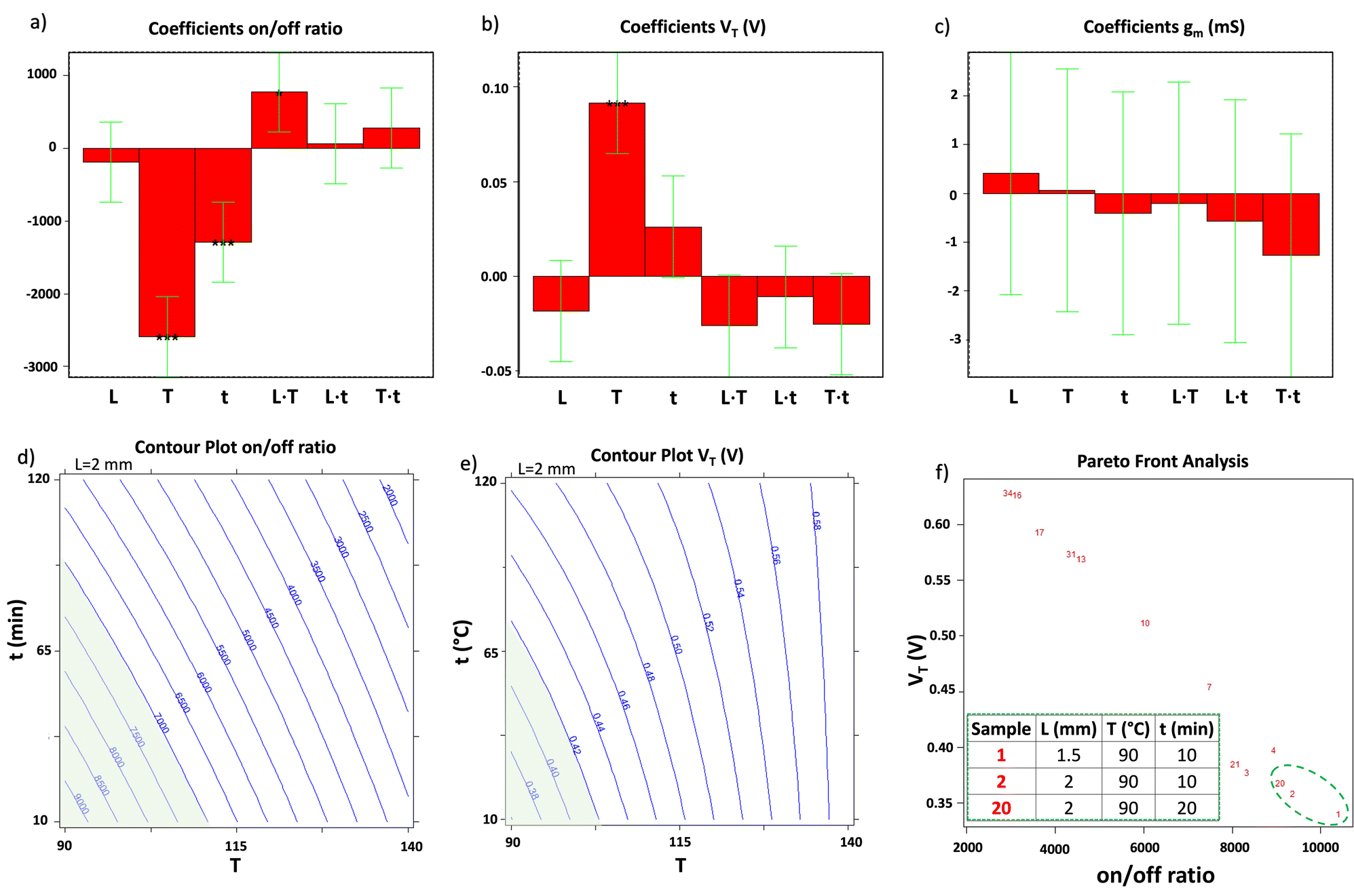
The transfer curve and output characteristics of this device are shown in Fig. 4. The optimized device can be switched off within the intended range, and the maximum gm of the device is near zero gate voltages (see Fig. 4(a)). The output characteristics, namely the IDvs. VD at IG ranging from 0.6 V to −0.6 V, also demonstrated high negative gate voltages and low positive gate voltages (inset, Fig. 4(b)). The annealing temperature of 90 °C and annealing time of 10 min with an L size of 2 mm, led to devices with a maximum on/off ratio of 8700 and an average gm of 22.5 ± 4.3. The average maximum transconductance peak was at −0.02 ± 0.08 V, and the average VT was 0.26 ± 0.03 V. The transfer curve with both sweeps is included in ESI,† Fig. S1.The time response (time constant) of the optimized device was measured and extracted using Bernards’ model63 (τ = 0.52 s), as shown in Fig. SI2 (ESI†), which is comparable with reported PEDOT:PSS based OECTs.64 In addition, EIS measurement was performed19,65 to estimate the channel capacitance (C = 0.5 mF) and volumetric capacitance (C* = 4 F cm−3), which is shown in Fig. SI3 (ESI†). This fabrication method, along with the optimization techniques, enabled the tuning of the OECTs operating range, reducing the gate voltages, which will be beneficial in case of having two power sources (VD and VG) in normal OECT setup or self-powered devices that ideally aim to use single power source.
 | ||
| Fig. 4 Electrical characterization of the optimized OECT device, fabricated with L = 2 mm, T = 90 °C, and t = 10 minutes. (a) Transfer characteristic (IDvs. VG ranging from 0.9 V to −0.6 V and VD = −0.4 V) along with transconductance curves. (b) Output characteristics of the device, namely IDvs. VD, ranging from 0 V to −0.6 V, with VG ranging from 0.6 V to −0.6 V. The results demonstrate the improved performance of the OECT under optimized fabrication conditions. | ||
Lastly, atomic force microscopy (AFM) characterization has been undertaken to analyze the channel morphology in the OECTs. Fig. 5 displays AFM topography images of four devices at different annealing conditions. Corresponding adhesion maps are shown in ESI,† Fig. S4. The topography images reveal that annealing temperature and time influence the stencil-printed PEDOT:PSS morphology. All topography in Fig. 5 shows surfaces characterized by a phase-segregated material comprising PEDOT:PSS grains surrounded by a shell formed by excess PSS.66 The PEDOT grains are characterized by a much higher intrinsic conductivity than the PEDOT-depleted grain boundary, being PSS which is a weaker ionic conductor. Zabihi et al.67 explained the change in nanograin morphology by that the thermal treatment of PEDOT:PSS leads to a change in morphology from granular to lamellar structures, increasing the electrical conductivity of their films. Moreover, no explicit materials contrast in adhesion or stiffness of the channels was observed. However, the thickness of the grain boundary has been found to depend on the annealing parameters.
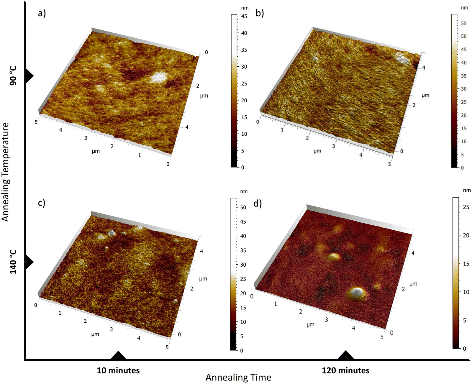 | ||
| Fig. 5 Representative 5 μm × 5 μm topography images of the channel region of 4 devices with L = 1.5 mm, and in (a) T = 90 °C and t = 10 minutes, (b) T = 90 °C and t = 120 minutes, (c) T = 140 °C and t = 10 minutes, (d) T = 140 °C and t = 120 minutes. | ||
In addition, the measured tip–surface adhesion was influenced by the heat treatment. The samples showed good materials homogeneity. However, on samples annealed at 90 °C, a lower adhesion was measured than those annealed at 140 °C (Fig. SI5, ESI†). It also indicated changes within the film, which drive the device's electrical performance, as seen in Fig. SI5 (ESI†). We observed that devices with lower threshold voltages tended to exhibit lower tip–surface adhesion, while devices with lower on/off ratios had higher tip–surface adhesion (see Fig. SI5, ESI†). The tip–sample adhesion results from interfacial, electrostatic, and capillary forces. Annealing conditions influence the size and density of PEDOT:PSS aggregates, which lead to the alteration of mobility and packing of the surface.68,69 Meanwhile, the electrical performance can be driven by other factors, such as device fabrication and channel thickness variations. Further investigation is needed to fully understand these effects and study the channel's bulk characteristics.
4. Conclusions
In conclusion, a simple and cost-effective fabrication and optimization method for developing a high-performing OECT is here reported. The OECT devices were fabricated and fully characterized based on a full factorial experimental design encompassing three variables: the annealing temperature, the annealing time, and the transistor channel length. The best experimental conditions allowing to minimize VT and maximize the on/off ratio have been determined by a Pareto-front multicriteria decision making. Moreover, it was observed that the transconductance of the devices is not significantly affected by the OECT design. Then, the morphology of OECT devices was investigated by AFM, which indicates the influence of annealing temperature and time. The next step for OECTs optimization can be implementing ultrasensitive biosensing applications. The approach herein undertaken can pave the way toward tuning the OECT electronic performance for the intended final application. Indeed, application-tuned OECTs can benefit surface characterization techniques reported earlier for switchable bio-surfaces.70 Lastly, tuning these devices will result in low-cost OECTs with optimized working performance for bioelectronics and biosensors.Conflicts of interest
The authors declare no conflict of interest.Acknowledgements
Staffan Dahlström for valuable discussions and assistance with the electrical measurement setup. Academy of Finland projects #316881, #316882, #316883 “Spatiotemporal control of Cell Functions”, Åbo Akademi CoE “Bioelectronic Activation of Cell Functions”, ERC Stg2021, GA:101040383, “NoOne-A binary sensor with single-molecule digit to discriminate biofluids enclosing zero or at least one biomarker”, Centro di Innovazione Regionale Digital Assay, funded by Regione PUGLIA Delibera Regionale n 702.08/11/2022 are acknowledged for financial support. Svenska Tekniska Vetenskapsakademien i Finland, and CSGI are acknowledged for partial financial support. In addition, Rosqvist acknowledges funding from Jane and Aatos Erkko Foundation (Project: ABC-Health). Bollella acknowledges Research for Innovation REFIN—Regione Puglia POR PUGLIA FESR-FSE 2014/2020 (6CDD3786).References
- R. A. Picca, K. Manoli, E. Macchia, L. Sarcina, C. Di Franco, N. Cioffi, D. Blasi, R. Österbacka, F. Torricelli, G. Scamarcio and L. Torsi, Ultimately Sensitive Organic Bioelectronic Transistor Sensors by Materials and Device Structure Design, Adv. Funct. Mater., 2020, 30, 1904513 CrossRef CAS.
- S. H. Kim, K. Hong, W. Xie, K. H. Lee, S. Zhang, T. P. Lodge and C. D. Frisbie, Electrolyte-gated transistors for organic and printed electronics, Adv. Mater., 2013, 25, 1822–1846 CrossRef CAS PubMed.
- D. Tu and S. Fabiano, Mixed ion-electron transport in organic electrochemical transistors, Appl. Phys. Lett., 2020, 117, 80501 CrossRef CAS.
- M. Berggren, X. Crispin, S. Fabiano, M. P. Jonsson, D. T. Simon, E. Stavrinidou, K. Tybrandt and I. Zozoulenko, Ion Electron–Coupled Functionality in Materials and Devices Based on Conjugated Polymers, Adv. Mater., 2019, 31, 1805813 CrossRef.
- J. Nissa, P. Janson, M. Berggren and D. T. Simon, The Role of Relative Capacitances in Impedance Sensing with Organic Electrochemical Transistors, Adv. Electron. Mater., 2021, 7, 2001173 CrossRef CAS.
- P. Romele, M. Ghittorelli, Z. M. Kovács-Vajna and F. Torricelli, Ion buffering and interface charge enable high performance electronics with organic electrochemical transistors, Nat. Commun., 2019, 10, 3044 CrossRef PubMed.
- E. Macchia, P. Romele, K. Manoli, M. Ghittorelli, M. Magliulo, Z. M. Kovács-Vajna, F. Torricelli and L. Torsi, Ultra-sensitive protein detection with organic electrochemical transistors printed on plastic substrates, Flexible Printed Electron., 2018, 3, 34002 CrossRef.
- F. Torricelli, D. Z. Adrahtas, F. Biscarini, A. Bonfiglio, C. A. Bortolotti, C. D. Frisbie, I. Mcculloch, E. Macchia and G. G. Malliaras, Electrolyte-gated transistors for enhanced performance bioelectronics, Nat. Rev. Methods Primers, 2021, 66 DOI:10.1038/s43586-021-00065-8.
- A. Marks, S. Griggs, N. Gasparini and M. Moser, Organic Electrochemical Transistors: An Emerging Technology for Biosensing, Adv. Mater. Interfaces, 2022, 9, 2102039 CrossRef CAS.
- P. C. Harikesh, C.-Y. Yang, D. Tu, J. Y. Gerasimov, A. M. Dar, A. Armada-Moreira, M. Massetti, R. Kroon, D. Bliman, R. Olsson, E. Stavrinidou, M. Berggren and S. Fabiano, Organic electrochemical neurons and synapses with ion mediated spiking, Nat. Commun., 2022, 13, 901 CrossRef CAS.
- Y. Liang, F. Brings, V. Maybeck, S. Ingebrandt, B. Wolfrum, A. Pich, A. Offenhäusser and D. Mayer, Tuning Channel Architecture of Interdigitated Organic Electrochemical Transistors for Recording the Action Potentials of Electrogenic Cells, Adv. Funct. Mater., 2019, 29, 1902085 CrossRef.
- A. Nawaz, Q. Liu, W. L. Leong, K. E. Fairfull-Smith and P. Sonar, Organic Electrochemical Transistors for In Vivo Bioelectronics, Adv. Mater., 2021, 33, 2101874 CrossRef CAS.
- J. Rivnay, P. Leleux, M. Sessolo, D. Khodagholy, T. Hervé, M. Fiocchi and G. G. Malliaras, Organic Electrochemical Transistors with Maximum Transconductance at Zero Gate Bias, Adv. Mater., 2013, 25, 7010–7014 CrossRef CAS.
- B. Piro, G. Mattana, S. Zrig, G. Anquetin, N. Battaglini, D. Capitao, A. Maurin and S. Reisberg, Appl. Sci., 2018, 8, 928 CrossRef.
- S. Chen, A. Surendran, X. Wu, S. Y. Lee, M. Stephen and W. L. Leong, Recent Technological Advances in Fabrication and Application of Organic Electrochemical Transistors, Adv. Mater. Technol., 2020, 5, 2000523 CrossRef CAS.
- F. Bonafè, F. Decataldo, I. Zironi, D. Remondini, T. Cramer and B. Fraboni, AC amplification gain in organic electrochemical transistors for impedance-based single cell sensors, Nat. Commun., 2022, 13, 1–9 Search PubMed.
- E. MacChia, R. A. Picca, K. Manoli, C. Di Franco, D. Blasi, L. Sarcina, N. Ditaranto, N. Cioffi, R. Österbacka, G. Scamarcio, F. Torricelli and L. Torsi, About the amplification factors in organic bioelectronic sensors, Mater. Horiz., 2020, 7, 999–1013 RSC.
- K. Lieberth, M. Brückner, F. Torricelli, V. Mailänder, P. Gkoupidenis and P. W. M. Blom, Monitoring Reversible Tight Junction Modulation with a Current-Driven Organic Electrochemical Transistor, Adv. Mater. Technol., 2021, 6, 2000940 CrossRef CAS.
- D. Ohayon, V. Druet and S. Inal, A guide for the characterization of organic electrochemical transistors and channel materials, Chem. Soc. Rev., 2023, 52, 1001–1023, 10.1039/D2CS00920J.
- P. R. Paudel, J. Tropp, V. Kaphle, J. D. Azoulay and B. Lüssem, Organic electrochemical transistors – from device models to a targeted design of materials, J. Mater. Chem. C, 2021, 9, 9761–9790 RSC.
- E. Zeglio and O. Inganäs, Active Materials for Organic Electrochemical Transistors, Adv. Mater., 2018, 30, 1800941 CrossRef.
- C. B. Nielsen, A. Giovannitti, D.-T. Sbircea, E. Bandiello, M. R. Niazi, D. A. Hanifi, M. Sessolo, A. Amassian, G. G. Malliaras, J. Rivnay and I. McCulloch, Molecular Design of Semiconducting Polymers for High-Performance Organic Electrochemical Transistors, J. Am. Chem. Soc., 2016, 138, 10252–10259 CrossRef CAS.
- C. J. Kousseff, R. Halaksa, Z. S. Parr and C. B. Nielsen, Mixed Ionic and Electronic Conduction in Small-Molecule Semiconductors, Chem. Rev., 2022, 122, 4397–4419 CrossRef CAS.
- P. R. Paudel, V. Kaphle, D. Dahal, R. K. Radha Krishnan and B. Lüssem, Tuning the Transconductance of Organic Electrochemical Transistors, Adv. Funct. Mater., 2021, 31, 2004939 CrossRef CAS.
- M. J. Donahue, A. Williamson, X. Strakosas, J. T. Friedlein, R. R. McLeod, H. Gleskova and G. G. Malliaras, High-Performance Vertical Organic Electrochemical Transistors, Adv. Mater., 2018, 30, 1705031 CrossRef.
- D. A. Koutsouras, F. Torricelli, P. Gkoupidenis and P. W. M. Blom, Efficient Gating of Organic Electrochemical Transistors with In-Plane Gate Electrodes, Adv. Mater. Technol., 2021, 6, 2100732 CrossRef CAS.
- C.-Y. Yang, D. Tu, T.-P. Ruoko, J. Y. Gerasimov, H.-Y. Wu, P. C. Harikesh, M. Massetti, M.-A. Stoeckel, R. Kroon, C. Müller, M. Berggren and S. Fabiano, Low-Power/High-Gain Flexible Complementary Circuits Based on Printed Organic Electrochemical Transistors, Adv. Electron. Mater., 2022, 8, 2100907 CrossRef CAS.
- Y. Yan, Q. Chen, X. Wu, X. Wang, E. Li, Y. Ke, Y. Liu, H. Chen and T. Guo, High-Performance Organic Electrochemical Transistors with Nanoscale Channel Length and Their Application to Artificial Synapse, ACS Appl. Mater. Interfaces, 2020, 12, 49915–49925 CrossRef CAS.
- S. Zhang, E. Hubis, G. Tomasello, G. Soliveri, P. Kumar and F. Cicoira, Patterning of Stretchable Organic Electrochemical Transistors, Chem. Mater., 2017, 29, 3126–3132 CrossRef CAS.
- A. Ait Yazza, P. Blondeau and F. J. Andrade, Simple Approach for Building High Transconductance Paper-Based Organic Electrochemical Transistor (OECT) for Chemical Sensing, ACS Appl. Electron. Mater., 2021, 3, 1886–1895 CrossRef CAS.
- S. Carli, M. Bianchi, M. Di Lauro, M. Prato, A. Toma, M. Leoncini, A. De Salvo, M. Murgia, L. Fadiga and F. Biscarini, Front. Mater., 2022, 9 DOI:10.3389/fmats.2022.1063763.
- U. Boda, I. Petsagkourakis, V. Beni, P. Andersson Ersman and K. Tybrandt, Fully Screen-Printed Stretchable Organic Electrochemical Transistors, Adv. Mater. Technol., 2023, 2300247 CrossRef CAS.
- M. Zabihipour, R. Lassnig, J. Strandberg, M. Berggren, S. Fabiano, I. Engquist and P. Andersson, Ersman, High yield manufacturing of fully screen-printed organic electrochemical transistors, npj Flex. Electron., 2020, 4, 15 CrossRef CAS.
- W. AlChamaa and M. Khraiche, High Performance Fully Inkjet-Printed Organic Electrochemical Transistor (OECT) Biosensor, J. Electrochem. Soc., 2022, 169, 87518 CrossRef CAS.
- A. Tricase, A. Imbriano, M. Valentino, N. Ditaranto, E. Macchia, C. Di Franco, R. Kidayaveettil, D. Leech, M. Piscitelli, G. Scamarcio, G. Perchiazzi, L. Torsi and P. Bollella, Water-Based Conductive Ink Formulations for Enzyme-Based Wearable, Biosensors, 2023, 2300036, 1–10 Search PubMed.
- S. T. M. Tan, G. Lee, I. Denti, G. LeCroy, K. Rozylowicz, A. Marks, S. Griggs, I. McCulloch, A. Giovannitti and A. Salleo, Tuning Organic Electrochemical Transistor Threshold Voltage using Chemically Doped Polymer Gates, Adv. Mater., 2022, 34, 2202359 CrossRef CAS.
- A. Håkansson, S. Han, S. Wang, J. Lu, S. Braun, M. Fahlman, M. Berggren, X. Crispin and S. Fabiano, Effect of (3-glycidyloxypropyl)trimethoxysilane (GOPS) on the electrical properties of PEDOT:PSS films, J. Polym. Sci., Part B: Polym. Phys., 2017, 55, 814–820 CrossRef.
- M. C. Tanese, D. Fine, A. Dodabalapur and L. Torsi, Interface and gate bias dependence responses of sensing organic thin-film transistors, Biosens. Bioelectron., 2005, 21, 782–788 CrossRef CAS.
- S. Cotrone, M. Ambrico, H. Toss, M. D. Angione, M. Magliulo, A. Mallardi, M. Berggren, G. Palazzo, G. Horowitz, T. Ligonzo and L. Torsi, Phospholipid film in electrolyte-gated organic field-effect transistors, Org. Electron., 2012, 13, 638–644 CrossRef CAS.
- J. G. Troughton, B. Marchiori, R. Delattre, S. Escoubas, M. Y. Aliouat, S. Grigorian and M. Ramuz, Simultaneous measurement of electrical characteristics and microstructure of crystallised PEDOT:PSS based OECTs under strain, Org. Electron., 2021, 92, 106108 CrossRef CAS.
- S. E. Doris, A. Pierre and R. A. Street, Dynamic and Tunable Threshold Voltage in Organic Electrochemical Transistors, Adv. Mater., 2018, 30, 1–5 CrossRef.
- Y. He, N. A. Kukhta, A. Marks and C. K. Luscombe, The effect of side chain engineering on conjugated polymers in organic electrochemical transistors for bioelectronic applications, J. Mater. Chem. C, 2022, 10, 2314–2332 RSC.
- G. Azzellino, A. Grimoldi, M. Binda, M. Caironi, D. Natali and M. Sampietro, Fully inkjet-printed organic photodetectors with high quantum yield, Adv. Mater., 2013, 25, 6829–6833 CrossRef CAS.
- F. Torricelli, I. Alessandri, E. Macchia, I. Vassalini, M. Maddaloni and L. Torsi, Green Materials and Technologies for Sustainable Organic Transistors, Adv. Mater. Technol., 2022, 7, 2100445, DOI:10.1002/admt.202100445.
- B. Holzer, K. Manoli, N. Ditaranto, E. Macchia, A. Tiwari, C. Di Franco, G. Scamarcio, G. Palazzo and L. Torsi, Characterization of Covalently Bound Anti-Human Immunoglobulins on Self-Assembled Monolayer Modified Gold Electrodes, Adv. Biosyst., 2017, 1, 1700055 CrossRef.
- E. Macchia, K. Manoli, B. Holzer, C. Di Franco, M. Ghittorelli, F. Torricelli, D. Alberga, G. F. Mangiatordi, G. Palazzo, G. Scamarcio and L. Torsi, Single-molecule detection with a millimetre-sized transistor, Nat. Commun., 2018, 9, 3223 CrossRef PubMed.
- B. Arman Kuzubasoglu and S. Kursun Bahadir, Flexible temperature sensors: A review, Sens. Actuators, A, 2020, 315, 112282 CrossRef CAS.
- G. Horowitz, P. Lang, M. Mottaghi and H. Aubin, Extracting parameters from the current–voltage characteristics of organic field-effect transistors, Adv. Funct. Mater., 2004, 14, 1069–1074 CrossRef CAS.
- E. Macchia, D. Alberga, K. Manoli, G. F. Mangiatordi, M. Magliulo, G. Palazzo, F. Giordano, G. Lattanzi and L. Torsi, Organic bioelectronics probing conformational changes in surface confined proteins, Sci. Rep., 2016, 6, 28085 CrossRef CAS.
- C. Di Franco, E. Macchia, L. Sarcina, N. Ditaranto, A. Khaliq, L. Torsi and G. Scamarcio, Extended Work Function Shift of Large-Area Biofunctionalized Surfaces Triggered by a Few Single-Molecule Affinity Binding Events, Adv. Mater. Interfaces, 2023, 10, 2201829, DOI:10.1002/admi.202201829.
- D. A. Koutsouras, M. H. Amiri, P. W. M. Blom, F. Torricelli, K. Asadi and P. Gkoupidenis, An Iontronic Multiplexer Based on Spatiotemporal Dynamics of Multiterminal Organic Electrochemical Transistors, Adv. Funct. Mater., 2021, 31, 2011013 CrossRef CAS.
- D. Blasi, F. Viola, F. Modena, A. Luukkonen, E. MacChia, R. A. Picca, Z. Gounani, A. Tewari, R. Österbacka, M. Caironi, Z. M. Kovacs Vajna, G. Scamarcio, F. Torricelli and L. Torsi, Printed, cost-effective and stable poly(3-hexylthiophene) electrolyte-gated field-effect transistors, J. Mater. Chem. C, 2020, 8, 15312–15321 RSC.
- R. Leardi, Experimental design in chemistry: A tutorial, Anal. Chim. Acta, 2009, 652, 161–172 CrossRef CAS.
- G. P. R. Leardi and C. Melzi, Gruppo di Chemiometria, CAT (Chemometric Agile Tool) freely downloadable from, https://gruppochemiometria.it/index.php/software, (accessed 9 January 2022).
- S. T. M. Tan, S. Keene, A. Giovannitti, A. Melianas, M. Moser, I. McCulloch and A. Salleo, Operation mechanism of organic electrochemical transistors as redox chemical transducers, J. Mater. Chem. C, 2021, 9, 12148–12158 RSC.
- O. Yaghmazadeh, F. Cicoira, D. A. Bernards, S. Y. Yang, Y. Bonnassieux and G. G. Malliaras, Optimization of organic electrochemical transistors for sensor applications, J. Polym. Sci., Part B: Polym. Phys., 2011, 49, 34–39 CrossRef CAS.
- Q. Tang, H. Li, M. He, W. Hu, C. Liu, K. Chen, C. Wang, Y. Liu and D. Zhu, Low threshold voltage transistors based on individual single-crystalline submicrometer-sized ribbons of copper phthalocyanine, Adv. Mater., 2006, 18, 65–68 CrossRef CAS.
- C. Scandurra, P. Bollella, R. Österbacka, F. Leonetti, E. Macchia and L. Torsi, Implementation of Experimental Design Techniques to Optimize Immunoglobulins detection with ultrasensitive sandwich immunoassays, Adv. Sens. Res., 2022, 1, 2200009, DOI:10.1002/adsr.202200009.
- B. Awadhiya, P. N. Kondekar, S. Yadav and P. Upadhyay, Insight into Threshold Voltage and Drain Induced Barrier Lowering in Negative Capacitance Field Effect Transistor, Trans. Electr. Electron. Mater., 2021, 22, 267–273 CrossRef.
- E. Macchia, F. Torricelli, P. Bollella, L. Sarcina, A. Tricase, C. Di Franco, R. Österbacka, Z. M. Kovács-Vajna, G. Scamarcio and L. Torsi, Large-Area Interfaces for Single-Molecule Label-free Bioelectronic Detection, Chem. Rev., 2022, 122, 4636–4699 CrossRef CAS PubMed.
- D. Khodagholy, J. Rivnay, M. Sessolo, M. Gurfinkel, P. Leleux, L. H. Jimison, E. Stavrinidou, T. Herve, S. Sanaur, R. M. Owens and G. G. Malliaras, High transconductance organic electrochemical transistors, Nat. Commun., 2013, 4, 2133, DOI:10.1038/ncomms3133.
- L. A. Sarabia, M. C. Ortiz and M. S. Sánchez, Response Surface Methodology, Elsevier, 2nd edn, 2020, vol. 1 Search PubMed.
- D. A. Bernards and G. G. Malliaras, Steady-State and Transient Behavior of Organic Electrochemical Transistors, Adv. Funct. Mater., 2007, 17, 3538–3544 CrossRef CAS.
- P. R. Paudel, M. Skowrons, D. Dahal, R. K. Radha Krishnan and B. Lüssem, The Transient Response of Organic Electrochemical Transistors, Adv. Theory Simul., 2022, 5, 1–15 Search PubMed.
- S.-M. Kim, C.-H. Kim, Y. Kim, N. Kim, W.-J. Lee, E.-H. Lee, D. Kim, S. Park, K. Lee, J. Rivnay and M.-H. Yoon, Influence of PEDOT:PSS crystallinity and composition on electrochemical transistor performance and long-term stability, Nat. Commun., 2018, 9, 3858 CrossRef.
- A. M. Nardes, M. Kemerink, R. A. J. Janssen, J. A. M. Bastiaansen, N. M. M. Kiggen, B. M. W. Langeveld, A. J. J. M. Van Breemen and M. M. De Kok, Microscopic understanding of the anisotropic conductivity of PEDOT:PSS thin films, Adv. Mater., 2007, 19, 1196–1200 CrossRef CAS.
- F. Zabihi, Y. Xie, S. Gao and M. Eslamian, Morphology, conductivity, and wetting characteristics of PEDOT:PSS thin films deposited by spin and spray coating, Appl. Surf. Sci., 2015, 338, 163–177 CrossRef CAS.
- S. Oras, S. Vlassov, M. Berholts, R. Lõhmus and K. Mougin, Tuning adhesion forces between functionalized gold colloidal nanoparticles and silicon AFM tips: role of ligands and capillary forces, Beilstein J. Nanotechnol., 2018, 9, 660–670 CrossRef CAS PubMed.
- B. D. Almquist and N. A. Melosh, Fusion of biomimetic stealth probes into lipid bilayer cores, Proc. Natl. Acad. Sci. U. S. A., 2010, 107, 5815–5820 CrossRef CAS.
- A. M. Ghafari, S. E. Domínguez, V. Järvinen, Z. Gounani, A. Schmit, M. Sjöqvist, C. Sahlgren, O. M. H. Salo-Ahen, C. Kvarnström, L. Torsi and R. Österbacka, In Situ Coupled Electrochemical-Goniometry as a Tool to Reveal Conformational Changes of Charged Peptides, Adv. Mater. Interfaces, 2022, 9, 2101480 CrossRef CAS.
Footnote |
| † Electronic supplementary information (ESI) available. See DOI: https://doi.org/10.1039/d3ma00888f |
| This journal is © The Royal Society of Chemistry 2023 |