DOI:
10.1039/D3MA00674C
(Paper)
Mater. Adv., 2023,
4, 6704-6717
Enhancing the perovskite solar cell performance by the interface modification of Zn–Sn–O compound heterostructures
Received
7th September 2023
, Accepted 20th November 2023
First published on 1st December 2023
Abstract
Enhancing the performance of perovskite solar cells (PSCs) is one of the prime concerns of researchers worldwide. For PSC devices, it is essential to develop the individual layer efficiently and cost-effectively. This work emphasizes the possibility of employing Zn–Sn oxide-based composite materials as alternative electron transport layers (ETLs) in PSC devices. Pristine Zn2SnO4 (ZTO), composite ZTO–ZnO, and ZTO–SnO2 heterostructure-based ETLs were prepared by a simple solid-state calcination technique and proposed as an alternative to the TiO2 photoanode used in PSC devices. The power conversion efficiency of the designed PSCs was studied based on crystallinity, morphology, cross-section, roughness, contact angle, work function, and Raman analysis of the ETL material. TEM analysis confirms the phase pure ZTO and heterostructure formation as a function of material stoichiometry. Compared to the pristine ZTO, the ZTO–ZnO and ZTO–SnO2 composites have enhanced PSC performance. The ZTO–SnO2 composites exhibit better band matching and charge transfer behavior with the perovskite layer than the pristine ZTO and ZTO–ZnO composites. The ZTO–SnO2 ETL-based PSC device displays a maximum efficiency of 15.9%, while ZTO–ZnO shows a maximum efficiency of 14.3%, which is more than 12.6% for the pristine ZTO. The results indicate that Zn2SnO4-based composites can be suitable for ETLs in PSC device fabrication.
1. Introduction
The need to transition from dependency on nonrenewable energy sources to renewable energy sources and to reduce global warming is a great concern.1,2 There are several energy conversion processes (solar cells, hydropower, wind power, nuclear power, and fuel cells) and energy storage (battery and supercapacitor) technologies are explored for this concern.1–5 Among them, the sun provides an enormous amount of energy (23![[thin space (1/6-em)]](https://www.rsc.org/images/entities/char_2009.gif) 000 TW) in a year compared to other renewable energy resources.1 By 2050, the world is estimated to need about 28 TW of electrical energy per year, which cannot be obtained from nonrenewable energy sources alone. In addition, the over-dependency on nonrenewable energy sources would lead to adverse effects like global warming.1 We must use technologies to trap and convert solar energy to valuable energy to solve this energy crisis.6 Although unlimited energy can be obtained from the sun, it requires efficient techniques to convert solar energy to electric power due to its low energy density. Photovoltaic technology has attained incredible consideration and has been utilized in various devices for the past few decades.7 Recent research reports that by 2030 the photovoltaic market is estimated to be about US$5 billion.8
000 TW) in a year compared to other renewable energy resources.1 By 2050, the world is estimated to need about 28 TW of electrical energy per year, which cannot be obtained from nonrenewable energy sources alone. In addition, the over-dependency on nonrenewable energy sources would lead to adverse effects like global warming.1 We must use technologies to trap and convert solar energy to valuable energy to solve this energy crisis.6 Although unlimited energy can be obtained from the sun, it requires efficient techniques to convert solar energy to electric power due to its low energy density. Photovoltaic technology has attained incredible consideration and has been utilized in various devices for the past few decades.7 Recent research reports that by 2030 the photovoltaic market is estimated to be about US$5 billion.8
Perovskite solar cells (PSCs) are a cost-effective solar energy harvesting technology because of their facile way of fabrication and efficient solar power conversion compared to other technologies.9 PSC technology is an effective way to develop a flexible energy source for wearable devices.10 Additionally, from the material point of view, perovskite materials exhibit unique properties like high absorption coefficients across the visible spectrum.9 The bandgap of the perovskite layer can be tuned by changing the material composition.9 PSC fabrication advanced initially from 2013 to 2022 through materials engineering processes.11 As a result, researchers had to work on materials engineering, and these efforts led to the development of a single junction PSC-certified efficiency of 25.5% under standard light illumination.12 Additionally, PSCs have the advantage of fabricating multijunction and tandem structures with Si-based solar cells and achieving higher conversion efficiency.13 However, when it comes to commercialization, the stability of PSCs is a significant concern.14 Researchers have been working on different ways to enhance the stability of PSCs.15
Recently, the interface modification of charge transport layers, the electron transport layer (ETL) and the hole transport layer (HTL), which play a pivotal role in PSC devices, has gained attention.16 The interface surface between the charge transport and perovskite layers has been chiefly studied to enhance the device's performance, especially by modifying the charge carrier injection, extraction, recombination, and ion migration at the interfaces.15 This is evident from several reports on improving the performance of PSC devices by modifying the ETL and HTLs.17,18 TiO2 is the more widely used ETL material in PSC devices.14 However, the TiO2 material is subjected to a post-deposition high temperature (∼550 °C) heat treatment process to achieve the desired anatase phase formation and surface modification like a mesoporous structure.19 This high-temperature preparation process is restricted for use in flexible devices.19 Also, the over-dependence on TiO2 for various applications has become a concern.20 Therefore, exploring non-toxic alternate ETL materials with low-temperature processing is necessary to replace the traditional TiO2 for PSC device fabrication.15 Metal oxides such as ZnO, SnO2, WO3, SrTiO3, and Zn2SnO4 were studied as alternatives to TiO2 ETLs in PSCs.21–25 Ashok et al. investigated Zn2SnO4 as an alternate ETL for improved power conversion efficiency (PCE) by modifying the surface features and obtained an efficiency of about 13.4%.26 Abuhelaiqa et al. studied the effect of a SnO2/TiO2 bilayer ETL to enhance charge carrier injection from the perovskite layer. They reported a considerable enhancement in fill factor (FF) and open circuit voltage (Voc) values along with decreased J–V hysteresis.27 In recent years researchers also explored heterostructure-based composite materials for ETL application due to their improved charge transport properties.28 Surface modification and band gap tuning processes have promoted charge transfer by minimizing the interfacial defects using heterostructures.27 Also, the heterostructure-based ETL improves the recombination process and charge transport resistance and enhances the stability of the devices.29 Sawanta et al. studied the charge carrier dynamics and transport behaviors of the perovskite layer and the top electrode by the interface engineering process to improve the device performance.30 Snaith et al. reported that the first few hundred hours of device performance are mainly affected by an electrical shunting mechanism of PSCs.31 The Zn–Sn-based composite heterostructure-based materials are also proposed for ETL application.32 The composite heterostructure materials exhibit better band matching with the perovskite layer. In addition to moisture resistance and chemical stability, ZTO-based metal oxides effectively block the hole transport toward the photoanode site and improve the device's performance.26 Also, the Zn–Sn–O-based composite heterostructure has various potential applications.32,33 Moreover, their excellent optoelectronic properties lead to enhanced charge transport properties.26 This improvement originates from heterostructure formation offering an effective charge transfer process at the perovskite–ETL interface.32
In this work, pristine ZTO, composite ZTO–ZnO, and ZTO–SnO2 heterostructures were studied as electron transport materials in PSC devices. The PCE of the fabricated PSCs was evaluated using the developed ZTO-based ETLs. The performance of the fabricated PSC devices was investigated based on the crystallinity, surface, optical, and electrical transport properties of the ETL material. An accelerated aging test was carried out to identify the stability of the fabricated devices. A possible transport mechanism between the perovskite and ETL is proposed based on the obtained results. The heterostructure provides a low-cost path to manufacture highly efficient and stable PSC devices.
2. Experimental methods and characterization
2.1. Materials and methods
Pristine ZTO, composite ZTO–ZnO, and ZTO–SnO2 heterostructures were synthesized by a simple solid-state calcination technique for ETLs in PSC devices. The detailed synthesis process has been reported in our earlier work.34 In brief, the required amount of zinc and tin metallic powders were ball milled for 12 h in ethanol media to obtain homogenous composite powders. Subsequently, the obtained powders were annealed at 950 °C for 8 h in the presence of oxygen to obtain the final products.
2.2. Characterization
The structural and morphological properties of the prepared powder composites were characterized using a high-resolution transmission electron microscope (HR-TEM) operated at 300 kV (ThermoFisher® Titan™ Themis) and analyzed using Image J software. The powder samples were dispersed in absolute ethanol by ultrasonication and drop-cast on amorphous carbon-coated copper grids for TEM analysis. Raman spectroscopy analysis (LabRam HR Evolution, Horiba) was performed to study the obtained product's vibrational properties and chemical composition. The spectra were recorded using a 532 nm laser from 100 to 800 cm−1. Before acquiring the spectra, calibration was performed using Si (520.7 cm−1) as a reference. The cross-section and surface morphology of the developed composite films were examined using field-emission scanning electron microscopy (FESEM; Carl Zeiss Supra 40 VP) and Focussed-Ion-Beam (FIB; ThermoFisher® Helios G4-UX). The surface features and roughness of the films were characterized by atomic force microscopy (AFM; ANTON PARR) with probe radius >10 nm and scan area of 15 × 15 μm2. A microscopic contact angle analyzer (OCA 50EC, Data Physics) assessed the wettability of the developed coatings in the static mode. The surface work function of the films was determined using a Kelvin Probe technique (Park NX20). All measurements were performed at room temperature. All measurements were performed at room temperature.
2.3. Fabrication of heterostructure ETL-based PSC devices
PSCs were developed with a normal (n–i–p) device structure on fluorine-doped tin oxide (FTO) coated glass substrates. Pristine ZTO, and composite ZTO–ZnO, ZTO–SnO2 heterostructure materials were used as ETLs to fabricate three different PSC devices. The ETLs were prepared as follows: 2 g of each prepared material (ZTO, ZTO–ZnO, and ZTO–SnO2) were individually mixed with 5 mL of ethanol (mixer), 0.2 mL of Triton X-100 (binder), and 0.5 mL of acetylacetone (solvent). The mixture was ground in an agate mortar pestle for one hour to obtain a homogeneous colloidal solution. Subsequently, the colloidal mixer was coated on FTO substrates (1.2 × 1.2 cm2) by the doctor blade technique. Then the coated samples were annealed at 500 °C for 30 min in a muffle furnace and naturally cooled to room temperature. The thickness of these different ETLs is optimized around 300 nm. The post-annealed photoanodes were treated with ozone for 10 min. Then the photoanodes were transferred to a glove box (VTI-vacuum technology) to deposit the perovskite (methylammonium lead iodide, MAPI) and hole transport layer (HTL) (Spiro-MeOTAD) by the spin coating method. The MAPI and Spiro-MeOTAD precursor solutions were prepared following a previous report.26 The thickness of the perovskite and HTL coatings was optimized via several trials. Finally, an Au electrode of thickness 120 nm was deposited by the thermal resistive evaporation method with a suitable mask. Three series of devices were fabricated and tested following similar fabrication procedures.
2.4. PSC testing
The power conversion efficiency (PCE, η%) of the different fabricated PSC devices was analyzed based on the photocurrent–voltage (J–V) characterization under AM1.5 illumination conditions using a Sol3A Class AAA Solar Simulator Measurements were conducted using a 150 W Xe lamp with a light intensity of 100 mW cm−2. An Oriel SRC1000TC cell was used for calibration. Electrochemical impedance spectroscopy (EIS) analysis was performed using an electrochemical workstation (PARSTAT4000A AMETEK Scientific Instruments) at 10 mV in the frequency range of 0.1 Hz to 1 MHz. The photo-stability of the fabricated PSCs was investigated in indoor environments. To understand the degradation mechanism of the fabricated PSCs, the cells were stored under continuous illumination using a white LED lamp. The performance of photovoltaic devices was evaluated periodically by the protocol adopted at the International Summit on Organic Photovoltaic Stability (ISOS).35
3. Results and discussion
3.1. Transmission electron microscopy analysis
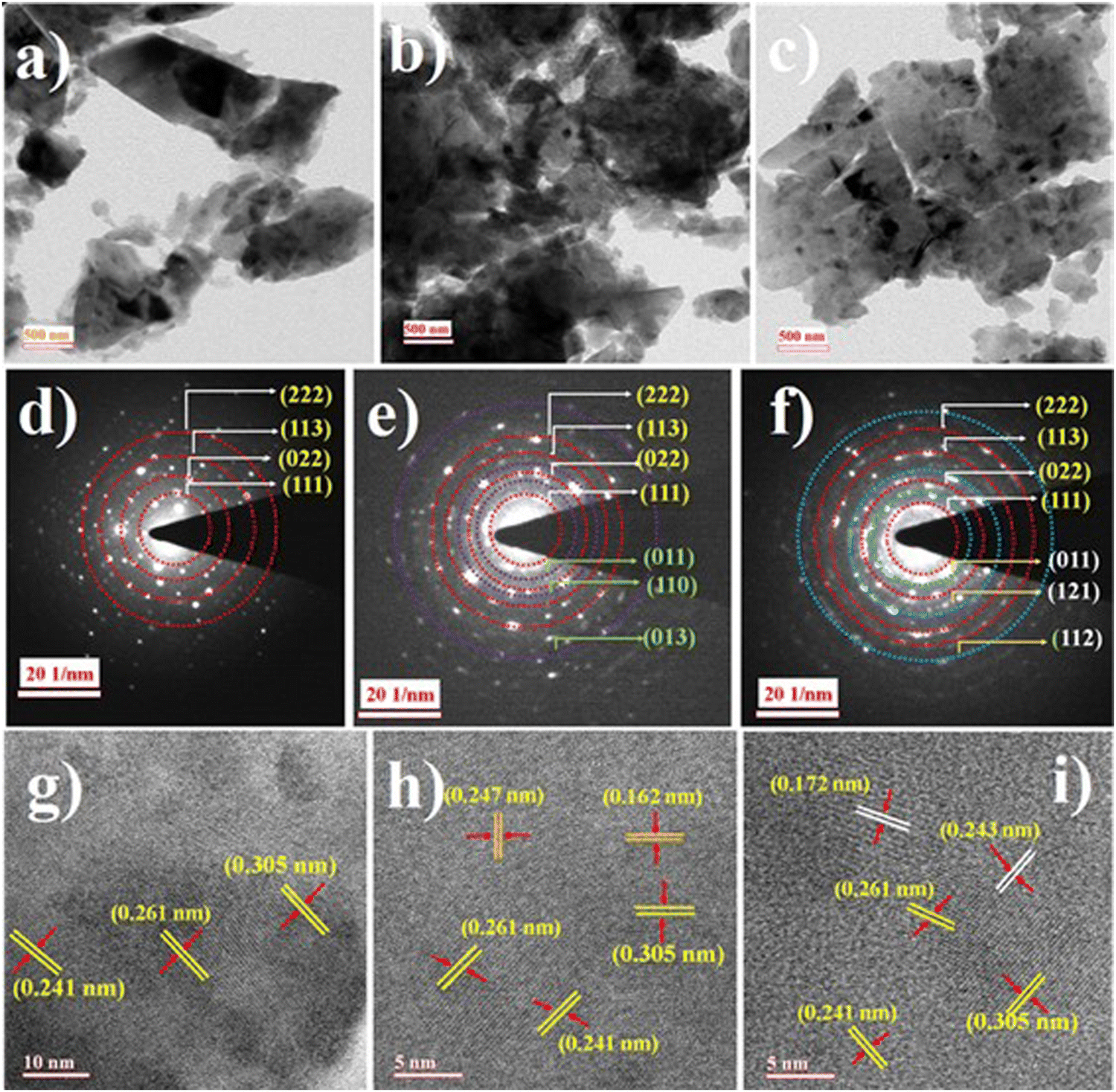
Fig. 1(a)–(c) show the HR-TEM micrographs of the synthesized ZTO, ZTO–ZnO, and ZTO–SnO2 powders. It can be observed that the synthesized powder samples have polyhedron structures with average crystallite dimensions above 500 nm. The composites ZTO–SnO2 and ZTO–ZnO have a relatively smaller crystallite size compared to ZTO. Due to the grain boundary effect, this smaller crystallite size might contribute to the effective charge transfer process.36 Selected area electron diffraction (SAED) pattern study was conducted to investigate the crystallinity and crystal structure of the systems. Fig. 1(d)–(f) display the obtained SAED patterns of ZTO, ZTO–ZnO, and ZTO–SnO2 powder samples. The pattern confirms the polycrystalline and heterostructure formation of the samples, as reported in our earlier publication.34 The obtained diffraction pattern of the pristine ZTO sample can be indexed as (111), (012), (113), and (222) planes of the cubic spinel structure of the Zn2SnO4 phase (JCPDS file No. 98-001-0595).37 In the case of ZTO–ZnO composite heterostructures, in addition to the Zn2SnO4 phase, diffraction patterns conforming to the (011), (110), and (013) planes of the hexagonal ZnO phase (ICSD code: 98-005-2827) can be observed.38 In the case of ZTO–SnO2 heterostructures, besides the Zn2SnO4 phase diffraction patterns corresponding to the (011), (121), and (112) planes of the cubic SnO2 phase (ICSD code: 98-006-5294)39 can be perceived. Moreover, the ZTO sample exhibits a highly intense bright spot indicating the higher crystalline nature. In comparison, ZTO–ZnO and ZTO–SnO2 samples exhibited bright rings, with multiple spots indicating the heterostructure formation.
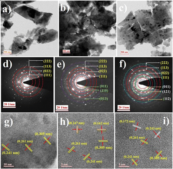 |
| | Fig. 1 Synthesized ZTO, ZTO–ZnO, and ZTO–SnO2 samples topological features from the TEM (a)–(c), SAED (d)–(f), and HR-TEM (g)–(i) images indicating the heterostructure formation. | |
Fig. 1(g) shows the HRTEM Bragg's pattern of the ZTO sample with the interlayer planer spacing of approximately 0.305, 0.261, and 0.241 nm conforming to the (111), (012), and (113) planes, respectively.37 Similarly, the HRTEM Bragg's pattern (Fig. 1(h) and (i)) of the ZTO–ZnO and ZTO–SnO2 heterostructure samples shows the presence of pristine ZTO planes along with the interplanar spacing of 0.247, 0.167 nm, and 0.243, 0.172 nm that can be attributed to the (110), and (013) planes of ZnO phase and (121), and (112) planes of SnO2 phase, respectively. Thus, the obtained results confirm the heterostructure formation, and it also shows that the final product's phase depends on the precursors' stoichiometric ratio. The heterostructure formation is known to play an effective role in the charge transfer process of optoelectronic devices.28 Samples with larger crystallite sizes lead to larger grains with a grain boundary.40 A polycrystalline crystal structure has effective grain boundaries that control the mobility of charge carriers. The presence of more significant grain boundaries can affect the charge carrier transport properties due to the scattering process.26 As a result, the stoichiometric ratios of the precursors can be adjusted to alter the charge transport properties of the samples.
3.2. Surface morphology analysis
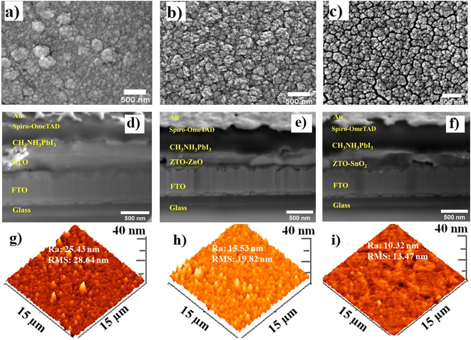
Fig. 2(a)–(f) depict the FESEM surface morphology images and Focussed-Ion-Beam (FIB) cross-sectional images of fabricated PSC devices with a planar device structure with different ETLs. ETLs of all the devices exhibited a polyhedral surface morphology, which significantly impacts the performance device.27 The FESEM images show a significant variation in surface morphologies based on their composition ratio (Fig. 2(a)–(c)). A sample with an excess of Zn content (ZTO–ZnO) has relatively bigger particles, whereas a Sn excess sample (ZTO–SnO2) shows homogeneous particle formation with dense film formation.34 In the case of the pristine sample agglomerated particle formation leads to more surface roughness which can significantly affect the charge transfer process of the devices. It has been reported that the surface roughness of the thin film effectively controls the charge transfer process of the PSC device.27,41 The cross-sectional FIB images exhibited significant variations in the cross-sectional film thickness due to the formation of different-sized particles.29 It is also noted that the ZTO–SnO2 film exhibited a relatively lower cross-sectional film thickness of 272 nm compared to other films. This high compactness of the film can facilitate the charge transfer process more effectively. The surface structure feature of ETLs strongly depends on Zn, Sn, and O elements in their stoichiometric ratio. However, the variation in the samples' stoichiometric ratio can create structural and surface defects. Generally, oxygen vacancies and/or ionic defects are the primary point defects in a metal oxide-based system.42 These defects also play an important role in charge transport properties.41
 |
| | Fig. 2 (a)–(c) FESEM surface morphology images of fabricated ZTO, ZTO–ZnO, and ZTO–SnO2 ETL-based perovskite solar cell devices, respectively. (d)–(f) FIB cross-sectional images of the ZTO, ZTO–ZnO, and ZTO–SnO2 ETLs used in PSC devices. (g)–(i) AFM images of ZTO, ZTO–ZnO, and ZTO–SnO2 coated on FTO substrates, respectively. | |
3.3. AFM analysis
Fig. 2(d)–(f) illustrate the AFM images of the 3D surface topography of the pristine ZTO, ZTO–ZnO, and ZTO–SnO2 composite heterostructures coated on FTO substrates. The significant impact of the heterostructures on surface topography compared to pristine samples was observed. The surface topography changes from needle-like to granular structures for pristine ZTO to heterostructure samples. Hence, the sample with a needle-like topography has a relatively higher surface roughness than that with a granular structure.43Fig. 2(d)–(f) show the sample's root mean square (RMS) roughness evaluated from the AFM data. The ZTO–SnO2 sample exhibited the lowest roughness value of about 13.47 nm. ZTO and ZTO–ZnO coatings showed higher roughness values of 28.46 and 19.82 nm, respectively, due to their needle-like surface structures. The RMS roughness and average roughness (Ravg) show similar variation for different ETL samples (Fig. 2(d)–(f)). These changes in the surface roughness might be due to the difference in the kinetics of grain growth during synthesis.44,45 Grain growth increases due to a decrease in the grain boundary effect. During film formation, two or more larger grains might combine to form a needle-like structure, contributing to surface roughness.45 The higher surface roughness of the films has a great impact on the charge transport process.44 It is reported that carrier mobility decreases due to the increased surface roughness of the film.44
3.4. Contact angle measurement
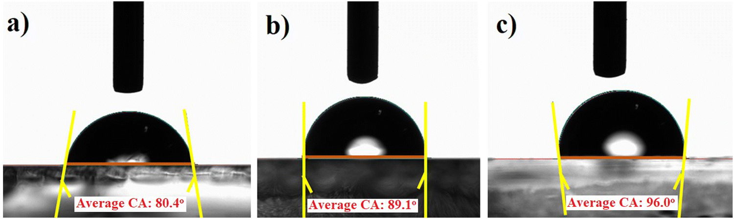
Climate change and moisture in the atmosphere significantly affect the performance of PSC devices.15 A contact angle measurement was carried out to examine the wettability of the coating and understand the stability of the fabricated devices upon exposure to water. Fig. 3(a)–(c) display the contact angles of water on ZTO, ZTO–ZnO, and ZTO–SnO2 samples coated over the FTO substrate. The average contact angles of ZTO, ZTO–ZnO, and ZTO–SnO2 coatings were 80.4, 89.1, and 96.0°, respectively. Generally, this high contact angle value indicates the strong hydrophobic behavior of the film, which means strong water-repelling behavior. However, this strong hydrophobic behavior of the ETL significantly influences the nucleation of the perovskite layer over the ETL.46 Also, it is reported that the higher contact angle leads to an improved energy barrier for heterogeneous nucleation.47 Hence, the charge transfer process at the ETL-perovskite interface is significantly affected by the higher contact angle value.47 Wen et al. reported that the surface-modified TiO2-based ETL shows a relatively low contact angle compared to a pristine TiO2-based device, which can facilitate the enhancement of the surface coverage of perovskite films.48 These measured contact angle values indicated that the surface morphology of the films has a strong impact. Contradictingly it is also reported that the higher contact angle-based HTLs presented enhanced PSC device performance compared to the lower contact angle HTL sample. FESEM analysis showed that the ZTO–SnO2 film is more compact compared to the pristine ZTO film. This highly compact nature of the heterostructure film may lead to a high contact angle value. A strong hydrophobic behavior of the film is more useful for preventing moisture penetration and controlling device degradation.49 Hence, the strong hydrophobic features of the ZTO–ZnO and ZTO–SnO2 heterostructures of the ETL can be more useful for inverted PSC structures to prevent moisture and improve the cell stability.
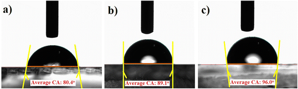 |
| | Fig. 3 Contact angle measurement of the synthesized (a) pristine ZTO, (b) ZTO–ZnO, and (c) ZTO–SnO2 samples coated over FTO substrates. | |
3.5. Surface work function analysis
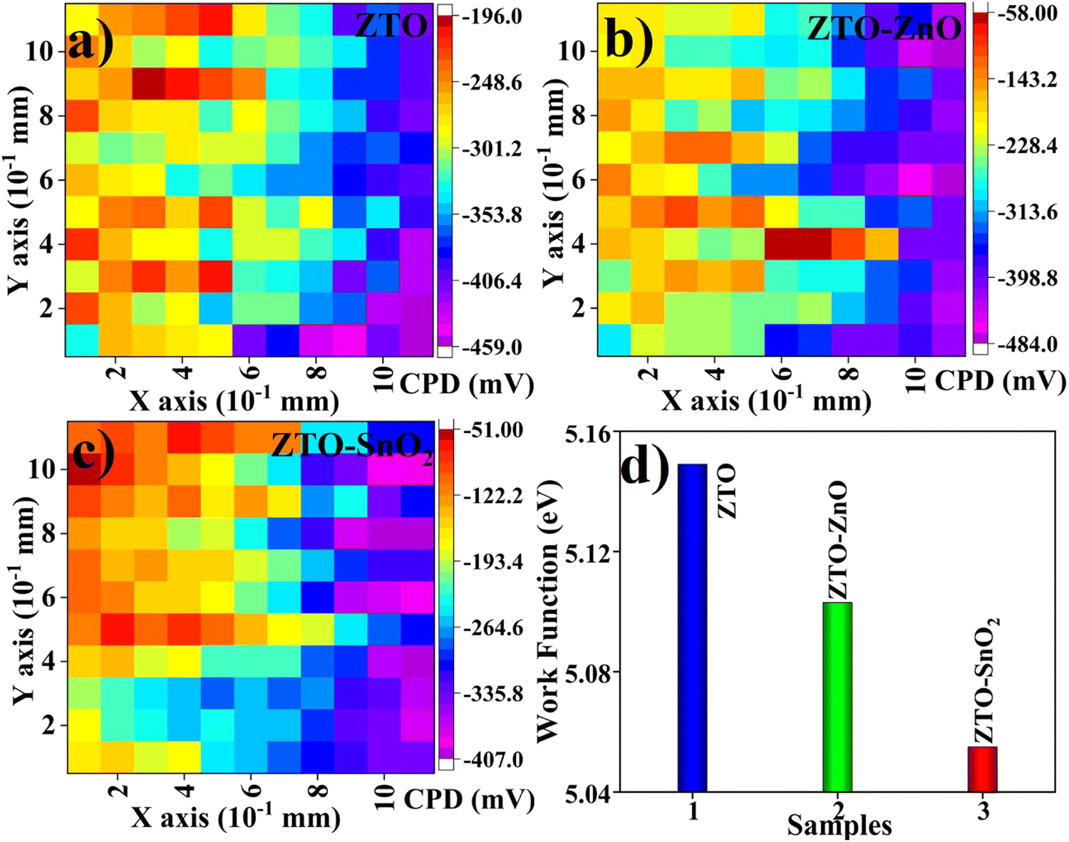
The surface work function (SWF) of the ETL plays an essential role in the charge transfer process in PSC devices.50 The surface work function of a semiconductor is defined as the energy level difference between the Fermi level concerning the vacuum level (ϕ = Evac − EF).50 In ETL materials, the valence band maximum, and the conduction band minimum can be modified by altering the band gap of the material by different material engineering processes.50 Also, the SWF can be altered due to variations in surface electronic properties.51 The Kelvin probe technique was used for the SWF of the ETL measurement by estimating the contact potential difference (CPD) values scanned over the film surface at room temperature. The CPD value (work function) is recorded for the reference electrode. Stainless steel was used as the reference electrode (work function = 4.83 eV). The working principle of a Kelvin probe is similar to AFM analysis in conduct mode.51 The variation of CPD of the film scanned over the 0.1 to 1 mm2 area range was recorded, and the acquired values were plotted as a contour map, as shown in Fig. 4(a)–(c). The SWF of the film was measured using the following relation.52
where ϕfilm is the SWF of the film, ϕRef is 4.83 eV, q is the electric charge and VCPD is the average CVD values scanned over the film surface. The different ETLs show a significant variation in VCPD values. The significant variation in VCPD values due to variations in the surface behavior of the films includes surface morphology, roughness, surface charge transport properties, etc.51 It is seen that the ZTO film exhibits more variation in VCPD values compared to heterostructure-based devices. The estimated average SWF of the ZTO film is 5.14 eV, ZTO–ZnO is 5.10, and ZTO–SnO2 is 5.05 eV (refer to Fig. 4(d)), and these values matched well with the previously reported values in the literature.53–55 Variation in the SWF of films arises due to a significant shift of the Fermi level towards the vacuum level based on the heterostructure formation compared to the pristine film. Also, the SWF of the ETL with the perovskite layer and bottom electrode layer effectively controls the carrier injection/transfer process.51–53 The obtained SWF values of the pristine and heterostructure-based ETL values suitable for the perovskite layer value (5.2 eV) and also the FTO electrode layer value (STD: 4.4 eV).56,57 Hence, the SWF study indicates the possible applicability of synthesized ZTO, composite ZTO–ZnO, and ZTO–SnO2 heterostructure samples as an ETL in a PSC device.
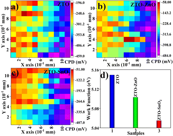 |
| | Fig. 4 Contact potential difference of (a) ZTO, (b) ZTO–ZnO, and (c) ZTO–SnO2 samples coated over the FTO substrates scanned over an area of 1 × 1 mm2. (d) The average surface work function of the ZTO, composite ZTO–ZnO, and ZTO–SnO2 heterostructure samples. | |
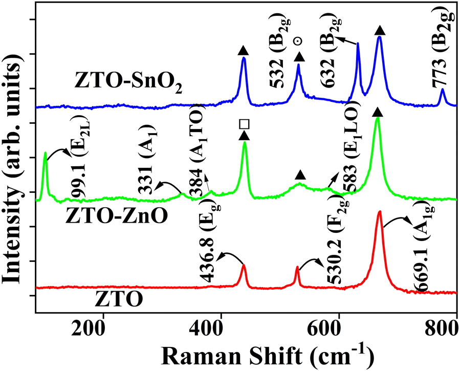
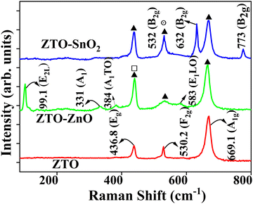
3.6. Raman analysis
The molecular vibrational modes and the surface functional group activity of the prepared pristine ZTO, composite ZTO–ZnO, and ZTO–SnO2 heterostructure systems were investigated through the Raman spectroscopy technique. Fig. 5 shows the obtained Raman active vibrational signals from the synthesized samples, which confirms the presence of Zn2SnO4, ZnO, and SnO2 phases. The intense peak at 669 cm−1 is related to the typical A1g symmetry of Zn2SnO4, which is the occurrence of the symmetric stretching of the Zn–O bonds in the ZnO4 tetrahedra of the cubic spinel Zn2SnO4.58 In addition, the other phonon modes at 530 cm−1 can be assigned to the F2g due to the symmetric bending of O atoms in the M–O bonds of the MO6 octahedra (M = Zn or Sn).59 The intense peak appearance at 438 cm−1 is analogous to the Eg mode related to the silent mode of Zn2SO4, and this peak position is also associated with the ZnO phase Raman-active mode (E2).59,60 In ZnO and SnO2 samples characteristic Raman active modes were absent in the pristine ZTO sample, thereby confirming the formation of a pure Zn2SnO4 phase. In contrast, ZTO–ZnO and ZTO–SnO2 heterostructures exhibited the dominant Zn2SnO4 phase-related peaks and the ZnO and SnO2 secondary phase peaks, respectively.
 |
| | Fig. 5 Raman spectra of synthesized ZTO, ZTO–ZnO, and ZTO–SnO2 heterostructure samples. | |
In the case of ZTO–ZnO, the vibrational mode detected near 99 cm−1 can be attributed to the vibrations of the zinc sublattice in ZnO.59,60 The peaks at 330 cm−1 and 379 cm−1 are due to the second-order vibration mode (E2L) and the A1 transverse-optical (TO) mode, respectively.60 The peak at 332 cm−1 is analogous to multi-phonon scattering processes. In contrast, the E1 longitudinal optical (LO) mode at 583 cm−1 can be attributed to oxygen defects such as vacancies or interstitials in ZnO.60 ZTO–SnO2 exhibits the characteristic Raman peaks at 632 cm−1 and 776 cm−1 that can be attributed to the A1g and B2g vibration modes, respectively.37 The vibration occurs in the A1g, B1g, and B2g modes in the plane perpendicular to the c-axis, while in the Eg mode in the direction of the c-axis.37 The observed Raman peaks from the ZTO–ZnO and ZTO–SnO2 samples indicate the heterostructure formation in the systems. Moreover, the spectrum of heterostructure-based samples shows a significant difference in the relative intensity and width of the vibrational peaks when compared with the pristine Zn2SnO4 sample. This confirms the heterostructure formation of the sample compared to a pristine ZTO sample.
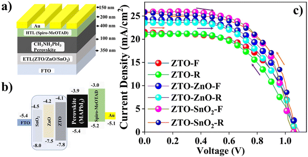
4. Perovskite solar cell testing
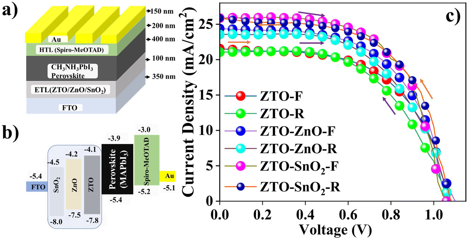
The performance of the pristine ZTO, composite ZTO–ZnO, and ZTO–SnO2 heterostructures as ETLs in PSCs was tested as an alternative to standard compact/mesoporous TiO2 materials. Fig. 6 shows the schematic of the fabricated PSC devices with different ETLs and appropriate layer thickness. The standard planar device structure (FTO/(ZTO/ZTO–ZnO/ZTO–SnO2)/MAPbI3/spiro-MeOTAD/Au) has been followed for all the devices.26 Band matching of each layer with the perovskite active layer is pictorially presented in Fig. 6(b). The J–V performances of the fabricated pristine ZTO, composite ZTO–ZnO, and ZTO–SnO2 heterostructure ETL-based PSC devices were compared. The J–V characterization of all the devices under forward and reverse-biased conditions is shown in Fig. 6(c). The active light exposure area of the fabricated PSC devices is around 2 × 2 mm2. The power of the incident light (100 mW cm−2) is kept constant for all the devices.
 |
| | Fig. 6 (a) Schematic representation of the fabricated ZTO/ZTO–ZnO/ZTO–SnO2 electron transport layers used in PSC devices with appropriate film thicknesses, (b) energy band diagram of the different ETL-based PSC device, and (c) J–V curves of the fabricated PSC device results compared with forward and reverse bias conditions. | |
4.1. Photocurrent–voltage (J–V) curve analysis
The power conversion efficiency (η) of pristine ZTO and ZTO–ZnO, ZTO–SnO2 composite heterostructure-based PSC devices was examined using the photovoltaic parameters, open-circuit voltage (Voc), short circuit current (Jsc), and fill factor (FF).26 The respective photocurrent–voltage (J–V) plot is shown in Fig. 6(c) with two different biasing conditions (forward and reverse). The estimated Voc, Jsc, and FF values are given in Table 1. Based on the obtained results of the studies on forward bias conditions, the pristine ZTO-based PSC device exhibits Voc = 1.12 V, Jsc = 21.5 mA cm−2, FF = 53.4, and η = 12.6%. In forward bias, it has been observed that the ZTO–ZnO composite-based device has Voc = 1.10 V, Jsc = 24.3 mA cm−2, FF = 53.6, and η = 14.3%. At the same time, the PSC device based on the ZTO–SnO2 composite structure displays Voc = 1.06 V, Jsc = 26.2 mA cm−2, F = 57.4, and η = 15.9%. In the case of the reverse bias condition, all the devices show significant variation and follow a similar profile to the forward bias condition. Hence, the ZTO–SnO2-based device shows a relatively improved photovoltaic behavior compared to ZTO–ZnO and pristine ZTO-based devices. An enhanced fill factor and current density were achieved due to a more surface-to-volume ratio of the dense and homogeneous surface morphology of the ZTO–SnO2 sample compared to the surface morphology of the ZTO–ZnO sample.34 The sheet-like surface morphology can promote effective charge transport at the interfaces between perovskite and ETL heterostructures.28 The multiband structure of the heterostructure with other layers can be another cause for improved efficiency.34 However, the devices' reverse biased J–V characteristic behavior showed relatively lower performance than the forward bias condition. These variations in the J–V curve indicate the hysteresis behavior of the device. Hysteresis can be due to the presence of several interfacial defects present in the device. The stability of a PSC device is easily affected by this hysteresis behavior.61 The heterostructure interface decreases J–V hysteresis due to the reduction of interfacial charge accumulation and improves charge carrier extraction.61 Also, it is reported that SnO2/TiO2-based heterostructure materials are introduced into the ETL for the stable change transport process to decrease the hysteresis behavior.27 Agresti et al. have studied the influence of light intensity on the current density with the n–i–p device structure.62 They reported that the Jsc becomes higher in the presence of the graphene–SnO2 heterostructure, which can reduce the hysteresis and enhance the charge extraction at the interface. The PSC device based on a standard TiO2 ETL has a Voc of 0.99 V, Jsc of 20.0 mA cm−2, FF of 73.0, and η of 15.0%.19 These values are relatively higher than our pristine ETL-based device since the pristine ETL-based device exhibits lower photovoltaic performance due to its low FF value. The low FF can facilitate the charge carrier recombination more effectively and decrease the current density.62 The higher sheet resistance of the photoanode material is also one of the causes of yielding a very low photocurrent density. The fabricated ZTO-based device result is compared with other heterostructure-based devices reported in the literature and summarised in Table 1.29,41,44,45,63–67
Table 1 Photovoltaic performance of pristine ZTO and composite ZTO–ZnO and ZTO–SnO2 heterostructure-based PSC devices with other reported heterostructure-based PSC devices
| Samples |
V
oc (mV) |
J
sc (mA cm−2) |
FF (%) |
η (%) |
Ref. |
| ZnO-F |
1.12 |
21.1 |
53.4 |
12.6 |
Present work |
| ZnO–R |
1.08 |
21.4 |
53.8 |
12.4 |
| ZnO–ZnO–F |
1.10 |
24.3 |
53.6 |
14.3 |
| ZnO–ZnO–R |
1.08 |
23.5 |
54.8 |
13.9 |
| ZnO–SnO2–F |
1.06 |
26.2 |
57.4 |
15.9 |
| ZnO–SnO2–R |
1.08 |
25.8 |
54.9 |
15.3 |
| TiO2–SnO2 |
1.04 |
23.2 |
66 |
15.9 |
29
|
| SnO2-TiO2 |
0.97 |
21.7 |
71 |
14.9 |
44
|
| SnO2–ZnO |
0.58 |
25.4 |
98.2 |
10.1 |
45
|
| ZnO–SnO2 |
1.15 |
21.74 |
76.4 |
19.1 |
41
|
| ZnO–ZnS |
1.12 |
24.1 |
76.6 |
20.7 |
63
|
| a-WOx/SnO2 |
1.11 |
22.9 |
80.15 |
20.44 |
64
|
| SnO2/CdS |
1.03 |
23.08 |
72.2 |
17.1 |
65
|
| Fe2O3@SnO2 |
1.6 |
7.88 |
80.85 |
10.23 |
66
|
| SnO2/BaSnO3 |
1.02 |
22.8 |
66.3 |
15.5 |
67
|
4.2. Charge transport mechanism of PSC devices
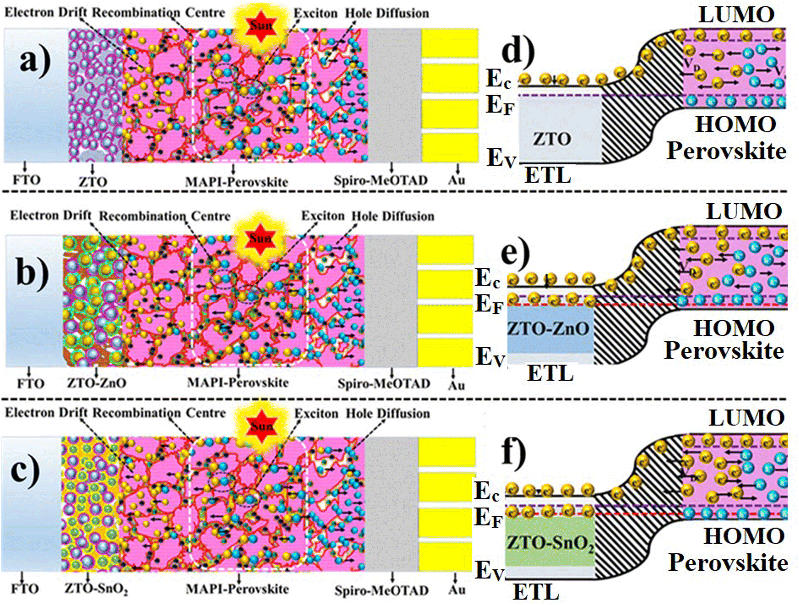
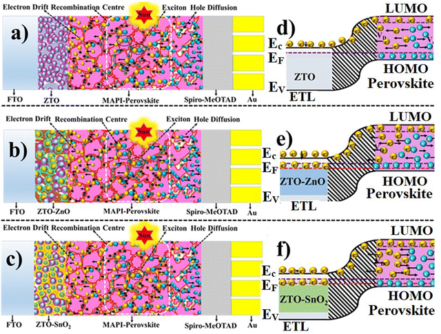
The charge transport mechanism of the fabricated PSC devices can be explained based on the charge transfer process of the ETL with a perovskite layer and conducting electrode layer. The pristine ZTO ETL-based PSC device exhibits a charge transport mechanism similar to that of a TiO2 ETL material-based PSC device.68 In a PSC device, sunlight illumination leads to the excitation of the carriers in the perovskite (MAPbI3) absorber from the HOMO to the LUMO level. During this process, these photo-excited charge carriers (exciton) separate in a fraction of a second. Subsequently, the separated charge carriers (electron/hole) are collected by the respective electrodes. Since, the power conversion efficiency of the PSC device strongly depends on the structural, surface morphology, and charge carrier transport process of the charge transport layers (ETL and HTL).26 Charge transport layers must control the charge carrier injection/extraction, recombination, and diffusion process more effectively. The ETL/HTL are in contact with the perovskite layer. Therefore, suitable band matching of the ETL/HTL can lead to better performance. In the case of a composite heterostructure-based device, the charge transport mechanism is different from that of the pristine ZTO-based PSC device. In a pristine ZTO ETL-based device, the charge carrier transfer from perovskite to the ZTO ETL is based on the single charge transfer process. Fig. 7(a) and (d) shows the cross-section schematics of the ZTO ETL-based PSC device structure and the energy band structure with the charge transfer process of the device. Effective electron carrier transport occurs from the LUMO level of the perovskite into the ETL conduction band (EC) during light illumination. Hence, the ETL charge transport properties effectively control the charge carrier collection of the photoanode. A pristine ZTO sample has relatively high charge transport resistance due to interfacial defects that affect carrier mobility.28 Also, a large amount of generated charge carriers from the perovskite absorber is accumulated at the interface due to the low carrier transfer ability of a pristine ZTO-based ETL. Such accumulation of charge carriers at the interface can facilitate recombination processes leading to low device performance. The ZTO–ZnO and ZTO–SnO2 composite heterostructure offers the multi-charge transfer process due to their multiband structure. Fig. 7(c)–(f) show the cross-section schematics of the ZTO–ZnO and ZTO–SnO2 ETL-based PSC device and the corresponding energy band structure with the charge transfer process. In heterostructure-based devices, charge transport occurs in two ways; charge transfer via the main ZTO phase and second is through the secondary phase of ZnO/SnO2.29 For example, in the ZTO–SnO2 heterostructure-based device, band matching occurs in two ways in the perovskite layer.34 Band matching between the perovskite-ZTO and perovskite–SnO2 phases offers two-way charge transfer processes. The multi-transfer process of this heterostructure effectively controls the charge carrier accumulation at the interface and hence regulates the recombination process.34 Also, it can be noted that the ZTO–SnO2 ETL-based PSC device exhibits better performance compared to the ZTO–ZnO-based device due to its sheet-like surface morphology.34 Therefore, the surface modification of the ETL influences the transfer process more effectively.34 Transferring the charges in dense surface structures is relatively more accessible than in in-homogeneous/agglomerated surface structures.
 |
| | Fig. 7 Schematic representation of pristine ZTO (a) and (b), ZTO–ZnO (c) and (d), and ZTO–SnO2 (e) and (f) heterostructure-based ETLs used in PSC device structures and with an appropriate energy band diagram with different ETLs. | |
The mobility of charge carriers is affected by the agglomerated surface structure, whereas in dense surface structures, charge transfer occurs more effectively. Hence, the heterostructure-based device has an advantage over the pristine device due to its effective charge transfer process.
4.3. Study of electrochemical impedance spectroscopy (EIS)
The charge transfer mechanism in the pristine ZTO and ZTO–ZnO, ZTO–SnO2 composite heterostructure-based PSC devices was investigated as a function of frequency using electrochemical impedance spectroscopy (EIS).69 A data acquired from the EIS measurement was further investigated using EC-Lab software. In the EC-Lab software, we process the experimental data with the most suitable equivalent circuit data analysis.69 An equivalent circuit is characterized based on the circuit elements like a capacitor, resistor, inductor, etc.70 The deviation of these elements was further analyzed from the constant phase elements (Q) and electric double-layer capacitors (Cdl).70 A constant phase element has a frequency-independent negative phase between current and voltage that interpolates between capacitors and resistors. Electric double-layer capacitors (Cdl) can be viewed as parallel circuits consisting of a large number of miniature capacitors with internal resistance.70Fig. 8(a) and (b) show the obtained Nyquist plots of the different ETLs, and the corresponding equivalent circuits. The high-frequency region of the real axis denotes the sheet resistance (Rs) between the photoanode and the perovskite interface. This low-frequency region denotes the diffusion resistance (R1) at the interface between the counter electrode and perovskite. The constant phase elements (Q) further analyzed the charge transport and diffusion resistance behavior. The Nyquist plot shows that all the devices exhibit a single semicircle. The higher frequency region from 1 MHz to 1 kHz shows a relatively smaller semicircle indicating the sheet resistance (Rs) of the pristine and heterostructure-based photoelectrodes. The second larger semicircle in the lower frequency, from 1 kHz to 1 Hz, presents more charge transport resistance at the perovskite–photoelectrode interface. Injection and collection of charge carriers are affected by higher charge transport resistance.71 However, no diffusion resistance is formed between the counter electrode and perovskite layer, indicating effective charge carrier collection. It is identified that the charge transport properties of the PSCs significantly changed with the heterostructure. The modified surface structure of the composite phase leads to a decrease in the charge transport resistance and diffusion resistance at the interface. The device fabricated with a heterostructure shows low sheet and charge transfer resistance, which might cause improved PCE compared to the pristine ZTO sample.72
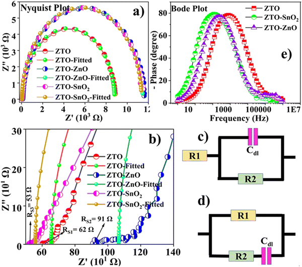 |
| | Fig. 8 (a) Electrochemical impedance spectra (Nyquist plot) of ZTO, ZTO–ZnO, and ZTO–SnO2 ETL-based PSC devices, (b) extended view of the Nyquist plot in the higher frequency range, (c) and (d) the equivalent circuit used for the J–V curve analysis, and (e) Bode plot of the fabricated devices. | |
The pristine ZTO ETL-based PSC device exhibits a much higher R1 value of 8734 Ω, leading to a decline in carrier mobility. The ZTO-based device shows a high Q value which indicates a relatively low charge collection at the counter electrode side. While the Q values of the heterostructure-based devices are lower, they exhibit improved charge carrier collection at the counter electrode.34 However, we do not deny that the lower charge transport resistance identified from the second semicircle region facilitates more charge carrier recombination, which is confirmed by lower Q values. The Bode plot provides an insight into the charge transport process more preciously.34 Notably, the Bode plot provides the lifetime of charge carriers using the following relation (τ) = 1/2pfmax, where fmax is the highest cut-off frequency.34Fig. 8(e) illustrates the Bode plots of the pristine ZTO and ZTO–ZnO, ZTO–SnO2 composite heterostructure-based PSC devices. From the plot, it can be estimated that the highest cut-off frequency of ZTO is 794 Hz, ZTO–ZnO is 251 Hz, and ZTO–SnO2 is 100 Hz. The determined lifetime of the charge carriers for the pristine ZTO, ZTO–ZnO, and ZTO–SnO2 heterostructure ETL-based devices is 1.2 ms, 3.9 ms, and 10 ms, respectively. The longer lifetime of the charge carriers in heterostructure-based devices effectively suppresses the charge carrier recombination process.29 ZTO-based devices also have a shorter lifetime compared with other devices. As a result, carrier density has decreased, and recombination resistance has been reduced at the interface between the photoanode and the electrolyte.27 However, decreasing interface resistance is one of the effective techniques to enhance the charge transfer process and avoid the recombinational process.27 It was primarily based on minimizing the charge carrier trap, and this trap is responsible for reducing perovskite efficiency. Thus, the obtained J–V curves and EIS measurements provide many hints for further improving the efficiency of the PSC device.
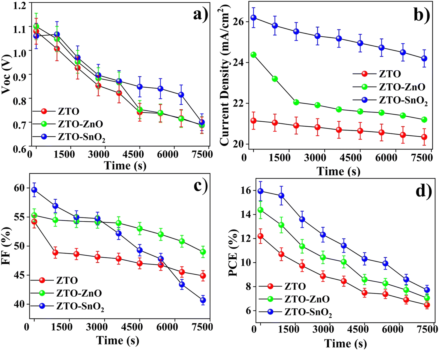
4.4. Stability analysis
Fig. 9 shows the stability analysis of the pristine ZTO and hybrid ZTO–ZnO, ZTO–SnO2 composite-based PSC devices. The ISOS-L-1 standard protocol was followed to explore the stability of the devices. The devices were illuminated with a lamp irradiated at 100 mW cm−2, at an ambient temperature and humidity of 24 ± 4 °C and 45 ± 5%, respectively.35 We measured the photovoltaic performance of the fabricated devices periodically and kept them under continuous illumination at all times. All the fabricated PSC devices decreased stability in the presence of light, similar to the observations of Huang et al.73
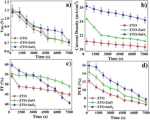 |
| | Fig. 9 (a) Stability egging test for the pristine ZTO, and composite ZTO–ZnO, ZTO–SnO2 heterostructure-based PSC devices; open-circuit voltage, (b) short circuit current, (c) fill factor, and (d) power conversion efficiency. | |
Under continuous lamp illumination, we observed significant decreases in the PSC devices' photovoltaic performance (Fig. 9(a)–(d)). Pristine ZTO-based PCE devices diminished with time due to decreased Jsc and FF levels. In the case of ZTO–ZnO and ZTO–SnO2 heterostructure-based PSC devices, a relatively low degradation was observed compared to the pristine ZTO-based device. Also, the electrode materials have not deteriorated strongly with time, as the Voc appeared to show low degradation.74 Degradation of the active layer and the device constituents was the primary cause of performance degradation. A reduction in Jsc and FF can be attributed to the photodegradation of perovskites. Photodegradation of organo-metal halide perovskite semiconductors is observed, although the degradation rate varies with the intensity of the incident light.29 Decomposition of perovskites into constituents results in the loss of optical and electrical properties.29,35
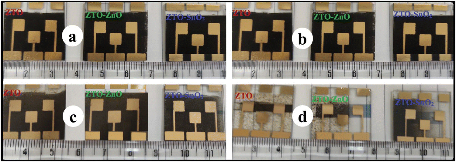
These results suggest that the photoanode side is relatively stable under white LED lamp illumination. In the long run, the decline in Voc and FF overtook the increase in Jsc, reducing PCE. Fig. 10 shows the visible degradation of the fabricated PSC devices. The photographs were taken following fabrication at 10, 20, and 30 day time intervals. It is identified that the fabricated PSC devices have a maximum lifetime of less than a month. However, making an encapsulation layer on top of devices can aid in improving the lifetime of the devices to some extent. Thus, the obtained stability results indicate the potential application of ZTO–ZnO and ZTO–SnO2 heterostructures as ETL materials for PSC device fabrication and a further improvement in the device performance.
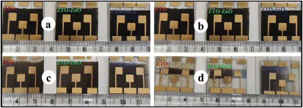 |
| | Fig. 10 Visible degradation of the pristine ZTO, and composite ZTO–ZnO, ZTO–SnO2 heterostructure-based PSC devices; (a) as-fabricated, (b) after 10 days, (c) after 20 days, and (d) after 30 days. | |
5. Conclusion
Pristine ZTO, composite ZTO–ZnO, and ZTO–SnO2 heterostructure systems were prepared by a simple solid-state calcination technique and employed as ETLs for PSC devices. The HR-TEM analysis confirms the crystallinity and its dependence on the stoichiometric ratio of the precursors. Synthesized samples exhibited a polyhedron surface morphology, which significantly impacts the change transport process of the PSC devices. The suitable surface work function of an ETL can facilitate effective charge carrier injection/collection, as well as control the recombination process. Perovskite solar cells fabricated using composite ZTO–ZnO and ZTO–SnO2 electron transport layers exhibited enhanced power conversion efficiency due to the multiband charge transport mechanism compared to the ZTO-based devices. Moreover, the PSC device based on ZTO–SnO2 exhibited a maximum efficiency of 15.9%, whereas ZTO–ZnO exhibited a maximum efficiency of 14.3%, which is relatively higher than the 12.6% for pristine ZTO. Hence, the results suggest that the ZTO–SnO2 heterostructure can be a potential ETL material for constructing stable PSC devices.
Conflicts of interest
The authors declare that they have no conflict of interests or personal relationships that could have appeared to influence the work reported in this paper.
Acknowledgements
Dr Ramarajan R. acknowledges the UGC Government of India for the financial assistance (Dr D. S. Kothari Postdoctoral Fellowship Program: Award letter number with data: F.4-2/2006(BSR)/PH/20-21/0152). The authors acknowledge the Department of Physics, IISc Bengaluru, India, Materials Research Centre, Ariel University, Israel, Advanced Facility for Microscopy and Microanalysis (AFMM), and the Centre for Nano Science and Engineering (CeNSE), IISc Bengaluru, for the fabrication and testing of the perovskite solar cell devices.
References
-
IRENA, World Energy Transitions Outlook: 1.5 °C Pathway, 2021 Search PubMed.
- J. Zhang, ES Energy Environ., 2021, 14, 1–2 Search PubMed.
- X. Jiang, Y. Chen, X. Meng, W. Cao, C. Liu, Q. Huang, N. Naik, V. Murugadoss, M. Huang and Z. Guo, Carbon, 2022, 191, 448–470 CrossRef CAS.
- G. Yuan, T. Wan, A. BaQais, Y. Mu, D. Cui, M. A. Amin, X. Li, B. Bin Xu, X. Zhu, H. Algadi, H. Li, P. Wasnik, N. Lu, Z. Guo, H. Wei and B. Cheng, Carbon, 2023, 212, 1–9 CrossRef.
- B. S. Boshoman, F. O. Fatoba and J. T. Jen, Eng. Sci., 2023, 1–14 Search PubMed.
-
J. Wang, R. Fu, S. Wen, P. Ning, M. H. Helal, M. A. Salem, B. Bin Xu, Z. M. El-Bahy, M. Huang, Z. Guo, L. Huang and Q. Wang, Progress and current challenges for CO2 capture materials from ambient air, Springer International Publishing, 2022, vol. 5 Search PubMed.
- T. Webb, S. J. Sweeney and W. Zhang, Adv. Funct. Mater., 2021, 31 Search PubMed.
- G. de, M. Jannuzzi and C. A. de Melo, Energy Sustainable Dev., 2013, 17, 40–46 CrossRef.
- C. Li, M. Feng, F. Guo, Q. Jiang, N. Li, Z. Guo and X. Liu1, Eng. Sci., 2022, 19, 1–4 Search PubMed.
- P. Zhang, S. Wu, Y. Chen, X. Li, F. Sun, M. Liu, Z. Chen and S. Li, Eng. Sci., 2022, 20, 180–187 CAS.
- N. G. Park, Nat. Sustainability, 2021, 4, 192–193 CrossRef.
- H. Min, D. Y. Lee, J. Kim, G. Kim, K. S. Lee, J. Kim, M. J. Paik, Y. K. Kim, K. S. Kim, M. G. Kim, T. J. Shin and S. I. Seok, Nature, 2021, 598, 444–450 CrossRef CAS PubMed.
- A. Harter, S. Mariotti, L. Korte, R. Schlatmann, S. Albrecht and B. Stannowski, Prog. Photovoltaics, 2023, 1–11 Search PubMed.
- J. W. Lee, T. Y. Lee, P. J. Yoo, M. Grätzel, S. Mhaisalkar and N. G. Park, J. Mater. Chem. A, 2014, 2, 9251–9259 RSC.
- J. Y. Kim, J. W. Lee, H. S. Jung, H. Shin and N. G. Park, Chem. Rev., 2020, 120, 7867–7918 CrossRef CAS PubMed.
- M. A. Haque, A. D. Sheikh, X. Guan and T. Wu, Adv. Energy Mater., 2017, 7, 1–23 CAS.
- J. Chen and N. G. Park, ACS Energy Lett., 2020, 5, 2742–2786 CrossRef CAS.
- Y. Liu, M. Bag, L. A. Renna, Z. A. Page, P. Kim, T. Emrick, D. Venkataraman and T. P. Russell, Adv. Energy Mater., 2016, 6, 1–7 Search PubMed.
- J. Burschka, N. Pellet, S. J. Moon, R. Humphry-Baker, P. Gao, M. K. Nazeeruddin and M. Grätzel, Nature, 2013, 499, 316–319 CrossRef CAS PubMed.
- S. N. A. Shah, Z. Shah, M. Hussain and M. Khan, Bioinorg. Chem. Appl., 2017, 1–12 Search PubMed.
- J. Kim, G. Kim, T. K. Kim, S. Kwon, H. Back, J. Lee, S. H. Lee, H. Kang and K. Lee, J. Mater. Chem. A, 2014, 2, 17291–17296 RSC.
- P. Wu, S. Wang, X. Li and F. Zhang, J. Mater. Chem. A, 2021, 9, 19554–19588 RSC.
- F. Ali, N. D. Pham, L. Fan, V. Tiong, K. Ostrikov, J. M. Bell, H. Wang and T. Tesfamichael, ACS Appl. Energy Mater., 2019, 2, 5456–5464 CrossRef CAS.
- K. Jung, J. Lee, C. Im, J. Do, J. Kim, W. S. Chae and M. J. Lee, ACS Energy Lett., 2018, 3, 2410–2417 CrossRef CAS.
- M. Neophytou, M. De Bastiani, N. Gasparini, E. Aydin, E. Ugur, A. Seitkhan, F. Moruzzi, Y. Choaie, A. J. Ramadan, J. R. Troughton, R. Hallani, A. Savva, L. Tsetseris, S. Inal, D. Baran, F. Laquai, T. D. Anthopoulos, H. J. Snaith, S. De Wolf and I. McCulloch, ACS Appl. Energy Mater., 2019, 2(11), 8090–8097 CrossRef CAS.
- A. Bera, A. D. Sheikh, M. A. Haque, R. Bose, E. Alarousu, O. F. Mohammed and T. Wu, ACS Appl. Mater. Interfaces, 2015, 7, 12404–12411 Search PubMed.
- M. Abuhelaiqa, N. Shibayama, X. X. Gao, H. Kanda and M. K. Nazeeruddin, ACS Appl. Energy Mater., 2021, 4, 3424–3430 CrossRef CAS.
- X. Xu, H. Zhang, J. Shi, J. Dong, Y. Luo, D. Li and Q. Meng, J. Mater. Chem. A, 2015, 3, 19288–19293 RSC.
- H. Guo, H. Zhang, J. Yang, H. Chen, Y. Li, L. Wang and X. Niu, ACS Appl. Energy Mater., 2018, 1, 6936–6944 CrossRef CAS.
- S. S. Mali, C. S. Shim, H. Kim and C. K. Hong, J. Mater. Chem. A, 2016, 4, 12158–12169 RSC.
- H. J. Snaith, A. Abate, J. M. Ball, G. E. Eperon, T. Leijtens, N. K. Noel, S. D. Stranks, J. T. W. Wang, K. Wojciechowski and W. Zhang, J. Phys. Chem. Lett., 2014, 5, 1511–1515 CrossRef CAS PubMed.
- R. Liu, W. Du, Q. Chen, F. Gao, C. Wei, J. Sun and Q. Lu, RSC Adv., 2013, 3, 2893–2896 RSC.
- M. Liu, H. Wu, Y. Wu, P. Xie, R. A. Pashameah, H. M. Abo-Dief, S. M. El-Bahy, Y. Wei, G. Li, W. Li, G. Liang, C. Liu, K. Sun and R. Fan, Adv. Compos. Hybrid Mater., 2022, 5, 2021–2030 CrossRef CAS.
- R. Ramanathan, M. Zinigrad, D. Kasinathan and R. K. Poobalan, ACS
Appl. Energy Mater., 2022, 5, 11506–11516 CrossRef CAS.
- A. K. Chauhan and P. Kumar, J. Mater. Sci.: Mater. Electron., 2019, 30, 9582–9592 CrossRef CAS.
- Y. Shao, Y. Fang, T. Li, Q. Wang, Q. Dong, Y. Deng, Y. Yuan, H. Wei, M. Wang, A. Gruverman, J. Shield and J. Huang, Energy Environ. Sci., 2016, 9, 1752–1759 RSC.
- S. Das and V. Jayaraman, Prog. Mater. Sci., 2014, 66, 112–255 CrossRef CAS.
- L.-B. Li, Y.-F. Wang, H.-S. Rao, W.-Q. Wu, K.-N. Li, C.-Y. Su and D.-B. Kuang, ACS Appl. Mater. Interfaces, 2013, 5, 11865–11871 CrossRef CAS PubMed.
- E. Samuel, T. G. Kim, C. W. Park, B. Joshi, M. T. Swihart and S. S. Yoon, ACS Sustainable Chem. Eng., 2019, 7, 14031–14040 CrossRef CAS.
- N. G. Park and H. Segawa, ACS Photonics, 2018, 5, 2970–2977 CrossRef CAS.
- D. Wang, C. Wu, W. Luo, X. Guo, B. Qu, L. Xiao and Z. Chen, ACS Appl. Energy Mater., 2018, 1, 2215–2221 CrossRef CAS.
- B. Roose, C. M. Johansen, K. Dupraz, T. Jaouen, P. Aebi, U. Steiner and A. Abate, J. Mater. Chem. A, 2018, 6, 1850–1857 RSC.
- F. Sadegh, S. Akin, M. Moghadam, V. Mirkhani, M. A. Ruiz-Preciado, Z. Wang, M. M. Tavakoli, M. Graetzel, A. Hagfeldt and W. Tress, Nano Energy, 2020, 75, 105038 CrossRef CAS.
- G. Martínez-Denegri, S. Colodrero, M. Kramarenko and J. Martorell, ACS Appl. Energy Mater., 2018, 1, 5548–5556 Search PubMed.
- Y. Li, F. Yang, Y. Wang, G. Shi, Y. M. Maung, J. Yuan, S. Huang and W. Ma, Sol. RRL, 2020, 4, 1–8 Search PubMed.
- Y. C. Liang and Y. Chao, RSC Adv., 2019, 9, 6482–6493 RSC.
- X. Gong, T. Wang, G. Yin, Q. Peng, Y. Chen, X. Wang, X. Qi, Y. Jiang, Z. Liu, Y. Shen and M. Wang, J. Mater. Chem. A, 2021, 9, 25567–25575 RSC.
- W. Wang, Z. Zhang, Y. Cai, J. Chen, J. Wang, R. Huang, X. Lu, X. Gao, L. Shui, S. Wu and J. M. Liu, Nanoscale Res. Lett., 2016, 11, 316 CrossRef CAS PubMed.
- Z. Liu, B. Sun, X. Liu, J. Han, H. Ye, Y. Tu, C. Chen, T. Shi, Z. Tang and G. Liao, J. Mater. Chem. A, 2018, 6, 7409–7419 RSC.
- W. Melitz, J. Shen, A. C. Kummel and S. Lee, Surf. Sci. Rep., 2011, 66, 1–27 CrossRef CAS.
- S. C. Dixon, D. O. Scanlon, C. J. Carmalt and I. P. Parkin, J. Mater. Chem. C, 2016, 4, 6946–6961 RSC.
- A. Klein, C. Körber, A. Wachau, F. Säuberlich, Y. Gassenbauer, R. Schafranek, S. P. Harvey and T. O. Mason, Thin Solid Films, 2009, 518, 1197–1203 CrossRef CAS.
- C. Liu, A. Piyadasa, M. Piech, S. Dardona, Z. Ren and P. X. Gao, J. Mater. Chem. C, 2016, 4, 6176–6184 RSC.
- R. Ramarajan, M. Kovendhan, K. Thangaraju, D. P. Joseph and R. R. Babu, Appl. Surf. Sci., 2019, 487, 1385–1393 CrossRef CAS.
- R. Jaramillo and S. Ramanathan, Adv. Funct. Mater., 2011, 21, 4068–4072 CrossRef CAS.
- C. Zhang, W. Luan and Y. Yin, Energy Procedia, 2017, 105, 793–798 CrossRef CAS.
- M. G. Helander, M. T. Greiner, Z. B. Wang, W. M. Tang and Z. H. Lu, J. Vac. Sci. Technol., A, 2011, 29, 011019 CrossRef.
- P. P. Das and P. Sujatha Devi, Inorg. Chem., 2014, 53, 10797–10799 CrossRef CAS PubMed.
- S. S. Mali, C. S. Shim and C. K. Hong, Sci. Rep., 2015, 5, 1–14 Search PubMed.
- D. Gültekin and H. Akbulut, Acta Phys. Pol., A, 2016, 129, 803–805 CrossRef.
- D. Lan, Prog. Photovoltaics, 2020, 28, 533–537 CAS.
- A. Agresti, A. Pazniak, S. Pescetelli, A. Di Vito, D. Rossi, A. Pecchia, M. Auf der Maur, A. Liedl, R. Larciprete, D. V. Kuznetsov, D. Saranin and A. Di Carlo, Nat. Mater., 2019, 18, 1228–1234 CrossRef CAS PubMed.
- R. Chen, J. Cao, Y. Duan, Y. Hui, T. T. Chuong, D. Ou, F. Han, F. Cheng, X. Huang, B. Wu and N. Zheng, J. Am. Chem. Soc., 2019, 141, 541–547 CrossRef CAS PubMed.
- F. Wang, Y. Zhang, M. Yang, J. Du, L. Xue, L. Yang, L. Fan, Y. Sui, J. Yang and X. Zhang, Nano Energy, 2019, 63, 1–8 Search PubMed.
- F. Mohamadkhani, S. Javadpour and N. Taghavinia, Sol. Energy, 2019, 191, 647–653 CrossRef CAS.
- R. Tui, H. Sui, J. Mao, X. Sun, H. Chen, Y. Duan, P. Yang, Q. Tang and B. He, J. Colloid Interface Sci., 2023, 640, 918–927 CrossRef PubMed.
- M. Kohan, T. Mahmoudi, Y. Wang, Y. H. Im and Y. B. Hahn, Appl. Surf. Sci., 2023, 613, 156068 CrossRef CAS.
- A. K. Jena, A. Kulkarni and T. Miyasaka, Chem. Rev., 2019, 119, 3036–3103 CrossRef CAS PubMed.
- D. Y. Son, K. H. Bae, H. S. Kim and N. G. Park, J. Phys. Chem. C, 2015, 119, 10321–10328 CrossRef CAS.
- A. Todinova, L. Contreras-Bernal, M. Salado, S. Ahmad, N. Morillo, J. Idígoras and J. J. A. Anta, ChemElectroChem, 2017, 4, 2891–2901 CrossRef CAS.
- B. R. Bade, K. B. Kore, S. R. Rondiya, D. S. Nilegave, M. P. Nasane, S. B. Jathar, S. V. Barma, S. R. Jadkar and A. M. Funde, ES Energy Environ., 2021, 13, 31–36 CAS.
- M. Spalla, E. Planes, L. Perrin, M. Matheron, S. Berson and L. Flandin, ACS Appl. Energy Mater., 2019, 2, 7183–7195 CrossRef CAS.
- H. Huang, J. Shi, L. Zhu, D. Li, Y. Luo and Q. Meng, Nano Energy, 2016, 27, 352–358 CrossRef CAS.
- S. B. Jathar, S. R. Rondiya, B. R. Bade, M. P. Nasane, S. V. Barma, Y. A. Jadhav, A. V. Rokade, K. B. Kore, D. S. Nilegave, P. U. Tandale, S. R. Jadkar and A. M. Funde, ES Mater. Manuf., 2021, 12, 72–77 CAS.
|
| This journal is © The Royal Society of Chemistry 2023 |
Click here to see how this site uses Cookies. View our privacy policy here. 
 Open Access Article
 This Open Access Article is licensed under a Creative Commons Attribution-Non Commercial 3.0 Unported Licence
 *b,
Chellakumar
R.
c,
K.
Ravichandran
c and
Michel
Zinigrad
a
*b,
Chellakumar
R.
c,
K.
Ravichandran
c and
Michel
Zinigrad
a