 Open Access Article
Optical properties of ZnFe2O4 nanoparticles and Fe-decorated inversion domain boundaries in ZnO†
S. B.
Kjeldby
 *a,
P. D.
Nguyen
a,
J.
García-Fernández
 a,
K.
Haug
 a,
A.
Galeckas
 a,
I. J. T.
Jensen
ab,
A.
Thøgersen
b,
L.
Vines
 a and
Ø.
Prytz
 a
a
aCentre for Materials Science and Nanotechnology, University of Oslo, N-0318 Oslo, Norway. E-mail: s.b.kjeldby@smn.uio.no
bSINTEF Industry, Sustainable Energy Technology, N-0314 Oslo, Norway
First published on 20th March 2023
Abstract
The maximum efficiency of solar cells utilizing a single layer for photovoltaic conversion is given by the single junction Shockley–Queisser limit. In tandem solar cells, a stack of materials with different band gaps contribute to the conversion, enabling tandem cells to exceed the single junction Shockley–Queisser limit. An intriguing variant of this approach is to embed semiconducting nanoparticles in a transparent conducting oxide (TCO) solar cell front contact. This alternative route would enhance the functionality of the TCO layer, allowing it to participate directly in photovoltaic conversion via photon absorption and charge carrier generation in the nanoparticles. Here, we demonstrate the functionalization of ZnO through incorporation of either ZnFe2O4 spinel nanoparticles (NPs) or inversion domain boundaries (IDBs) decorated by Fe. Diffuse reflectance spectroscopy and electron energy loss spectroscopy show that samples containing spinel particles and samples containing IDBs decorated by Fe both display enhanced absorption in the visible range at around 2.0 and 2.6 eV. This striking functional similarity was attributed to the local structural similarity around Fe-ions in spinel ZnFe2O4 and at Fe-decorated basal IDBs. Hence, functional properties of the ZnFe2O4 arise already for the two-dimensional basal IDBs, from which these planar defects behave like two-dimensional spinel-like inclusions in ZnO. Cathodoluminescence spectra reveal an increased luminescence around the band edge of spinel ZnFe2O4 when measuring on the spinel ZnFe2O4 NPs embedded in ZnO, whereas spectra from Fe-decorated IDBs could be deconvoluted into luminescence contributions from bulk ZnO and bulk ZnFe2O4.
1 Introduction
ZnO is a wide band gap (3.3 eV![[thin space (1/6-em)]](https://www.rsc.org/images/entities/char_2009.gif) 1) semiconductor with a hexagonal wurtzite crystal structure which is used in a wide range of applications,2,3 including as a transparent conducting oxide (TCO).4,5 For photovoltaics, absorption in nanoparticles can permit efficient generation of multiple charge carriers for absorption of photons with energies higher than twice the band gap, a process which is typically inefficient in bulk materials.6 Nanoparticles embedded in a TCO are of particular interest, since this design could facilitate extraction of the optically generated charge carriers via the nanoparticle-TCO heterojunction.7 In addition, this design allows the TCO layer to actively participate in solar energy conversion, effectively turning the TCO layer into the top cell in a tandem-like solar cell. Previous research has demonstrated that it is possible to form Ge nanoparticles7 or Zn2GeO4 nanoparticles8 in ZnO by ion implantation followed by annealing. The same synthesis method can also be used to form SiO2 nanoparticles in Ga2O3.9 In the current work, we examine similar samples fabricated via a powder synthesis route.
1) semiconductor with a hexagonal wurtzite crystal structure which is used in a wide range of applications,2,3 including as a transparent conducting oxide (TCO).4,5 For photovoltaics, absorption in nanoparticles can permit efficient generation of multiple charge carriers for absorption of photons with energies higher than twice the band gap, a process which is typically inefficient in bulk materials.6 Nanoparticles embedded in a TCO are of particular interest, since this design could facilitate extraction of the optically generated charge carriers via the nanoparticle-TCO heterojunction.7 In addition, this design allows the TCO layer to actively participate in solar energy conversion, effectively turning the TCO layer into the top cell in a tandem-like solar cell. Previous research has demonstrated that it is possible to form Ge nanoparticles7 or Zn2GeO4 nanoparticles8 in ZnO by ion implantation followed by annealing. The same synthesis method can also be used to form SiO2 nanoparticles in Ga2O3.9 In the current work, we examine similar samples fabricated via a powder synthesis route.
The reported phase diagram of the Zn–Fe–O system indicates that for cation ratios in excess of ∼2% it is possible to form spinel ZnFe2O4 nanoparticles (NPs) in ZnO,10 which has also been experimentally confirmed.11 In normal spinel ZnFe2O4, i.e. with an inversion parameter of zero, Zn2+ occupies tetrahedral sites, and Fe3+ occupies octahedral sites sharing edges. ZnFe2O4 is a semiconductor with a bandgap of about 2.0 eV12. In two junction tandem solar cells with a silicon bottom cell, the optimal top cell band gap is 1.7–1.8 eV, depending on device architecture.13 If the top cell is composed of a TCO functionalized with embedded semiconducting nanoparticles, the nanoparticles should consequently have a band gap of around 1.7–1.8 eV. Since ZnFe2O4 has a bandgap close to these values, ZnFe2O4 NPs could be appropriate for TCO functionalization. The optical properties of bulk ZnFe2O4 and ZnFe2O4 nanoparticles have been previously investigated by photoluminescence spectroscopy12,14,15 and diffuse reflectance spectroscopy (DRS).16 The stabilisation of heterostructures of ZnFe2O4 nanoparticles embedded in ZnO has attracted attention, particularly for their magnetic properties and photocatalytic activity.11,17,18 The possibility of embedding nanoparticles of ZnFe2O4 in ZnO combined with the band gap value of ZnFe2O4 makes this phase a good candidate for functionalization of bulk and thin film ZnO.
Several transition metal impurities, like In or Fe, can promote formation of the inversion domain boundary (IDB) microstructure in ZnO.19–22 Inversion domains in ZnO are planar defects across which the wurtzite c-axis orientation is rotated 180°.21 Two different types of IDBs are found in the IDB microstructure. Basal IDBs (b-IDBs) lie parallel to the ZnO-(0001) planes and have a head-to-head configuration (c-axes in the bordering grains point toward each other).21 Pyramidal IDBs (p-IDBs) lie parallel to the ZnO-{2![[1 with combining macron]](https://www.rsc.org/images/entities/char_0031_0304.gif)
![[1 with combining macron]](https://www.rsc.org/images/entities/char_0031_0304.gif) 5} or {
5} or {![[2 with combining macron]](https://www.rsc.org/images/entities/char_0032_0304.gif) 115} planes and have tail-to-tail configuration (c-axes of neighboring grains point away from each other).21 For sufficiently high Fe-concentrations, iron tends to occupy octahedral sites on b-IDBs or trigonal bipyramidal sites on p-IDBs,21,23 referred to as Fe-decoration of the IDBs. On b-IDBs, it has been reported that the decoration can result in a completely filled close-packed iron monolayer embedded in the ZnO matrix.21 The structure of the ZnO IDBs has been studied extensively by microscopic techniques,20,24,25 and the elemental composition has been investigated with core-loss electron energy loss spectroscopy (EELS) and energy dispersive X-ray spectroscopy (EDS).21,23 However, little attention has been paid to the low-loss range of the EELS spectrum, which contains information about the dielectric response of the sample. Similarly, optical characterization of the structures remains scarce. The effect of such a regular defect structure on functional properties certainly warrants further investigation. Additionally, the local configuration of Fe-ions is similar at Fe-decorated b-IDBs and in normal spinel, including similar Fe–O bond lengths.26 Functional similarities could arise from such structural similarities.
115} planes and have tail-to-tail configuration (c-axes of neighboring grains point away from each other).21 For sufficiently high Fe-concentrations, iron tends to occupy octahedral sites on b-IDBs or trigonal bipyramidal sites on p-IDBs,21,23 referred to as Fe-decoration of the IDBs. On b-IDBs, it has been reported that the decoration can result in a completely filled close-packed iron monolayer embedded in the ZnO matrix.21 The structure of the ZnO IDBs has been studied extensively by microscopic techniques,20,24,25 and the elemental composition has been investigated with core-loss electron energy loss spectroscopy (EELS) and energy dispersive X-ray spectroscopy (EDS).21,23 However, little attention has been paid to the low-loss range of the EELS spectrum, which contains information about the dielectric response of the sample. Similarly, optical characterization of the structures remains scarce. The effect of such a regular defect structure on functional properties certainly warrants further investigation. Additionally, the local configuration of Fe-ions is similar at Fe-decorated b-IDBs and in normal spinel, including similar Fe–O bond lengths.26 Functional similarities could arise from such structural similarities.
In the present work, we have studied the functional and structural properties of Fe-decorated IDBs in ZnO and spinel ZnFe2O4 NPs embedded in ZnO. This study complements previous structural characterization of the IDB microstructure, and explores similarities and differences in the functional behavior of the IDB microstructure and the embedded nanoparticles.
2 Experimental procedures
Samples were prepared by a powder synthesis route where powders of ZnO (Sigma Aldrich 99.99%) and α-Fe2O3 (Sigma Aldrich 99.5%) were mixed to arrive at a 10% cation ratio (Fe/(Zn + Fe)) for samples 1 and 2. The powders were ball milled in isopropanol using an agate jar and 10 mm agate balls for 2 hours at 300 rpm. The resulting mixtures were pressed into pellets measuring 13 mm in diameter, which were loaded into a furnace at 1400 °C and allowed to homogenize for between 4 and 17 hours. According to the phase diagrams,10 the iron is fully incorporated into the wurtzite matrix in a solid solution at this temperature. The pellets were left in the furnace to cool to room temperature over a 5 hour period. One of the pellets was subjected to a second heat treatment at 1000 °C for 36 hours (sample 1). Samples were cut from the middle of the pellets. Two additional samples were prepared with nominal compositions ZnFe2O4 (sample 3) and ZnO (sample 4). An overview of the samples can be found in Table 1. For clarity, samples are henceforth referred to by the label given in the table.| Sample | Sample label | Nominal composition | Annealing |
|---|---|---|---|
| 1 | Nanocomposite | Zn0.9Fe0.1O1.05 | 1400 °C for 12 h |
| +1000 °C for 36 h | |||
| 2 | IDB sample | Zn0.9Fe0.1O1.05 | 1400 °C for 4 h |
| 3 | Bulk ZnFe2O4 | ZnFe2O4 | 1400 °C for 17 h |
| 4 | Bulk ZnO | ZnO | 1400 °C for 12 h |
The samples were characterized by X-ray diffraction (XRD) on the pellet samples, (scanning) transmission electron microscopy ((S)TEM) and optical measurements. XRD data were obtained in a Rigaku MiniFlex600 diffractometer with a Cu Kα1 source. Electron transparent cross-sectional TEM samples were prepared by mechanical grinding, polishing, and final thinning by Ar ion milling in a Gatan PIPS II (Model 695). Structures were initially investigated using selected area electron diffraction (SAED) and STEM techniques in a JEOL JEM 2100F operated at 200 kV. Subsequently, atomic-resolution structural characterization and EDS studies were carried out using a Thermo Fisher Scientific Cs-corrected Titan G2 60–300 kV microscope equipped with a Wien-filter monochromator, Gatan GIF Quantum 965 EELS spectrometer and Super-X EDS detectors. The microscope was operated at 300 kV accelerating voltage, and the probe-forming optics were configured to form a ∼0.8 Å probe with a convergence semi-angle of 22 mrad. The semi-angular ranges of the high-angle annular dark field (HAADF) and annular bright field (ABF) detectors were 100–200 and 10–20 mrad, respectively. Additionally low-loss EELS was performed at 60 kV using a collection semi-angle of 21 mrad. The acquisition at 60 kV acceleration voltage reduces the impact of retardation effects, which may otherwise complicate the determination of the bandgap. The energy dispersion was 0.01 eV per channel. The energy resolution measured using the full width at half maximum (FWHM) of the zero-loss peak was 0.18 eV. Principle component analysis (PCA)27 with 20 components was used to reduce spectral noise.
In EELS, the energy loss of high-energy electrons transmitted through a sample is measured. This energy loss is caused by interactions between the electron and the sample and gives information about sample composition (core-loss EELS) or optical properties such as the band gap (low-loss EELS). Low-loss EELS measurements require a monochromated electron beam as good energy resolution is needed. Importantly, low-loss EELS permits characterization of band gap variations on length scales down to approximately 10 nm,28,29 providing vastly superior spatial resolution to conventional optical techniques. The high spatial resolution makes low-loss EELS an excellent technique for characterizing optical properties of samples containing nanoparticles.
Sample absorption properties were characterized using DRS and low-loss EELS. Room temperature DRS data were collected using an EVO-600 (Thermo Fisher Scientific, Inc.) UV-Vis spectrophotometer. Sample emission properties were characterized with cathodoluminescence (CL) in a JEOL IT-300 SEM, equipped with an Andor SR 193i spectrograph and an Andor Newton CCD detector. CL spectra were acquired at 80 K, at accelerating voltages from 10 to 15 kV, and were averaged over the region of interest. A smoothing filter was applied to reduce noise. X-ray photoelectron spectroscopy (XPS) was used to study the compositional elements in the different samples. The XPS analysis was performed in a KRATOS AXIS ULTRA DLD instrument (Kratos Analytical Ltd, Manchester, UK) using monochromatic Al Kα radiation (hv = 1486.6 eV).
3 Results
Fig. 1 displays locked-coupled X-ray diffractograms from the pellet samples between 28 and 52° for all samples. As expected, diffractograms from the nanocomposite, the IDB sample and the bulk ZnO sample revealed diffraction peaks from ZnO. The nanocomposite and the bulk ZnFe2O4 sample had diffraction peaks from ZnFe2O4. Interestingly, the IDB sample displayed a small shift toward lower angles for the ZnO-(10![[1 with combining macron]](https://www.rsc.org/images/entities/char_0031_0304.gif) 1) peak, and a splitting of the ZnO-(0002) peak. The (0002) peak with low intensity (34.45°) is close to the ZnO-(0002) peak from the bulk ZnO sample. The higher intensity peak appears at a smaller angle (34.05°), indicating elongation of the ZnO c-axis in this sample, which will be discussed further later. Additionally, we observe additional peaks at around 35.5 and 47.1°. A diffraction peak similar to the former was previously observed in similarly prepared samples.30 Potential candidates for the peak at 35.5° are magnetite (Fe3O4) or maghemite (γ-Fe2O3), for which strong diffraction peaks have been observed around this angle (ICSD 77588 and ICSD 172906), although other diffraction peaks from these phases were not observed. Alternatively, this low-intensity diffraction peak could be due to a small volumetric portion of ZnFe2O4, with the (311) diffraction peak shifted by 0.3° relative to the bulk ZnFe2O4. At the surface of the IDB sample, a small portion of ZnFe2O4 might be expected, due to Zn evaporation during heat treatment. However, the ZnFe2O4 phase was not observed in the TEM data from the IDB sample.
1) peak, and a splitting of the ZnO-(0002) peak. The (0002) peak with low intensity (34.45°) is close to the ZnO-(0002) peak from the bulk ZnO sample. The higher intensity peak appears at a smaller angle (34.05°), indicating elongation of the ZnO c-axis in this sample, which will be discussed further later. Additionally, we observe additional peaks at around 35.5 and 47.1°. A diffraction peak similar to the former was previously observed in similarly prepared samples.30 Potential candidates for the peak at 35.5° are magnetite (Fe3O4) or maghemite (γ-Fe2O3), for which strong diffraction peaks have been observed around this angle (ICSD 77588 and ICSD 172906), although other diffraction peaks from these phases were not observed. Alternatively, this low-intensity diffraction peak could be due to a small volumetric portion of ZnFe2O4, with the (311) diffraction peak shifted by 0.3° relative to the bulk ZnFe2O4. At the surface of the IDB sample, a small portion of ZnFe2O4 might be expected, due to Zn evaporation during heat treatment. However, the ZnFe2O4 phase was not observed in the TEM data from the IDB sample.
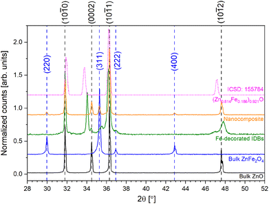 | ||
| Fig. 1 Diffractograms from all samples in Table 1. A zero-point shift has been applied. Peak positions for ZnFe2O4 and ZnO have been indicated by dotted lines and indices (blue for ZnFe2O4, black for ZnO). The pink dotted line shows the diffractogram from an Fe-rich ZnO solid solution obtained from ICSD (ICSD: 155784). | ||
SEM-EDS data confirmed that the composition of the nanocomposite and the IDB sample was spatially homogeneous, please see the ESI† for further details. Secondary electron and backscatter electron imaging in SEM also revealed the presence of voids in these samples.
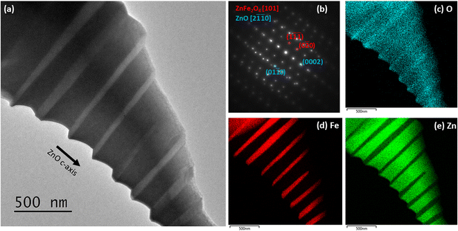
To investigate the microscopic structure of the samples, STEM and EDS characterization was conducted. In Fig. 2(a), the bright field STEM image from the nanocomposite reveals bright rod-like particles embedded in a dark ZnO matrix. The crystal structure and chemical composition of the particles were determined through SAED and EDS mapping respectively, see Fig. 2(b)–(e). The data confirmed that the particles were composed of spinel ZnFe2O4. This identification is consistent with our XRD data, and is in line with what was expected from published phase diagrams,10 which indicate formation of the spinel phase at the annealing temperature and composition of the nanocomposite. The particles have undergone solid state growth, and are embedded in the ZnO matrix with their [111] axis parallel to the polar ZnO [0001] axis. The aspect ratios of the particles show a clear preferential growth in the [121] direction.
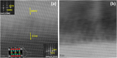
Fig. 3(a) and (b) show simultaneously acquired HAADF and ABF STEM images of an interface between ZnO and a spinel ZnFe2O4 nanoparticle in the nanocomposite. In Fig. 3(a), fast Fourier transforms (FFTs) for both phases and the projected atomic model of ZnFe2O4 superposed on the magnified HAADF STEM image from the spinel particle are shown in the insets. From the FFTs, we find the lattice matching relation ZnO [0001]‖ZnFe2O4 [![[1 with combining macron]](https://www.rsc.org/images/entities/char_0031_0304.gif)
![[1 with combining macron]](https://www.rsc.org/images/entities/char_0031_0304.gif) 1], which is in agreement with the SAED data. The interface appears slightly diffuse in both the ABF and HAADF images. This could be due to the presence of strain and misfit dislocations at the mismatched interfacial region, a situation which was recently reported for spinel ZnCr2O4 nanoparticles embedded in ZnO by geometric phase analysis.31
1], which is in agreement with the SAED data. The interface appears slightly diffuse in both the ABF and HAADF images. This could be due to the presence of strain and misfit dislocations at the mismatched interfacial region, a situation which was recently reported for spinel ZnCr2O4 nanoparticles embedded in ZnO by geometric phase analysis.31
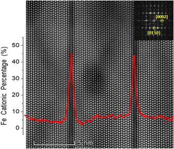
Fig. 4 shows a HAADF STEM image of the IDB sample along the ZnO-[2![[1 with combining macron]](https://www.rsc.org/images/entities/char_0031_0304.gif)
![[1 with combining macron]](https://www.rsc.org/images/entities/char_0031_0304.gif) 0] zone axis. It is known from the literature that b-IDBs are visible in this zone axis, while p-IDBs are not resolved clearly.22 The overlaid EDS profile of Fe in cation atomic percent reveals increased Fe concentration at the b-IDBs. The EDS data also revealed decreased Zn concentration at the b-IDBs (not shown). In HAADF, the contrast is heavily influenced by the atomic number and density of the sample. This gives dark contrast at the Fe-decorated b-IDBs in the HAADF image, since they have higher concentrations of the lighter Fe atoms and lower concentrations of the heavier Zn atoms than the surrounding ZnO grains. Convergent beam electron diffraction from the same area (not shown) confirmed that the polarity of the ZnO grains was indeed inverted across the b-IDBs. These observations are in line with previous studies.22,23
0] zone axis. It is known from the literature that b-IDBs are visible in this zone axis, while p-IDBs are not resolved clearly.22 The overlaid EDS profile of Fe in cation atomic percent reveals increased Fe concentration at the b-IDBs. The EDS data also revealed decreased Zn concentration at the b-IDBs (not shown). In HAADF, the contrast is heavily influenced by the atomic number and density of the sample. This gives dark contrast at the Fe-decorated b-IDBs in the HAADF image, since they have higher concentrations of the lighter Fe atoms and lower concentrations of the heavier Zn atoms than the surrounding ZnO grains. Convergent beam electron diffraction from the same area (not shown) confirmed that the polarity of the ZnO grains was indeed inverted across the b-IDBs. These observations are in line with previous studies.22,23
Fe cationic concentrations around 5 and 45% were observed in the ZnO grains and the b-IDBs respectively. The observed Fe-concentrations at the b-IDBs is relatively low compared to the literature, where a full Fe monolayer at b-IDBs has been reported.21 This is attributed to partial Zn-occupation at the b-IDBs, minor sample inhomogeneity, or scattering effects. Due to scattering, the electron beam spreads while passing through the sample. Hence, even when the electron beam is positioned directly on an IDB, some of the EDS signal originates from the neighboring ZnO grains. Consequently, scattering effects are expected to lower the observed Fe concentrations at the b-IDBs. Analogously, scattering effects would increase the observed Fe concentration in ZnO grains.
The b-IDBs are of primary interest in the current work, but observations of iron-decoration of p-IDBs can be found in the ESI (Fig. S3†). In normal spinel ZnFe2O4, Zn and Fe are tetrahedrally and octahedrally coordinated, respectively. XPS data (see the ESI, Fig. S4†), show some tetrahedrally coordinated Fe in the nanocomposite, revealing a small but non-zero inversion parameter in this sample. From the XPS data, we find that Fe is octahedrally coordinated in the IDB sample, similar to what is found for the bulk ZnFe2O4 sample.
As stated previously, the ZnO-(0002) peak was split in the IDB sample, with one low intensity peak at 34.45° and a high intensity peak at 34.05°, see Fig. 1. For the high intensity peak, a qualitatively similar shift was observed in previous work by Yamashita et al. for Fe-rich ZnO.32 For a solid solution containing 18.6 cation atomic percent Fe (pink line in Fig. 1), the ZnO-(0002) and (10![[1 with combining macron]](https://www.rsc.org/images/entities/char_0031_0304.gif) 2) diffraction peaks are shifted to around 33.8 and 47.1° in the data from Yamashita et al. Comparing with our data, we find that presence of Fe-rich ZnO can account for the XRD peaks at 34.05 and 47.1°. Since we observe smaller shifts than Yamashita et al., particularly for the ZnO-(0002) peak, the solid solution is likely less Fe-rich in our case, which is reasonable since the IDB sample had a nominal composition of 10 cation atomic percent Fe. The low-intensity ZnO-(0002) peak is attributed to ZnO grains with low Fe concentration, where the reduced Fe concentration is caused by accumulation of Fe at the IDBs. The low intensity of this diffraction peak reveals that these grains are either small or make up a small volumetric fraction of the sample.
2) diffraction peaks are shifted to around 33.8 and 47.1° in the data from Yamashita et al. Comparing with our data, we find that presence of Fe-rich ZnO can account for the XRD peaks at 34.05 and 47.1°. Since we observe smaller shifts than Yamashita et al., particularly for the ZnO-(0002) peak, the solid solution is likely less Fe-rich in our case, which is reasonable since the IDB sample had a nominal composition of 10 cation atomic percent Fe. The low-intensity ZnO-(0002) peak is attributed to ZnO grains with low Fe concentration, where the reduced Fe concentration is caused by accumulation of Fe at the IDBs. The low intensity of this diffraction peak reveals that these grains are either small or make up a small volumetric fraction of the sample.
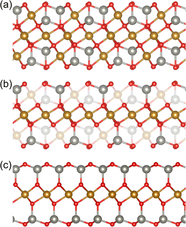
Spinel ZnFe2O4 features atomic layers of Fe octahedrally coordinated by O on {111} planes. Fe-decorated b-IDBs in ZnO consist of a single layer of Fe octahedrally coordinated by O on ZnO basal planes ((0001) planes). A schematic representation is given in Fig. 5. As can be seen from the figure, the two structures are similar up to the closest neighbors of the Fe-atoms, while there are differences in the second closest neighbors of the Fe-atoms. Based on this observation, it is interesting to investigate whether the structural similarity gives rise to functional similarities. We therefore focus on characterizing the optical properties of spinel ZnFe2O4 NPs and Fe-decorated IDBs in ZnO in the remainder of this work.
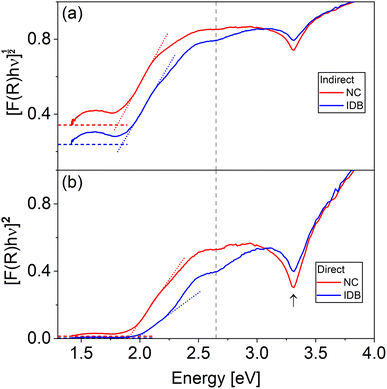
In Fig. 6, DRS Tauc plots assuming direct and indirect transition are shown for the nanocomposite and IDB sample. The plots reveal clear similarities between the two samples, with the absorption band edge slightly below 2 eV for both samples. At 3.2 eV, the spectra show a decrease, followed by a sharp increase from ∼3.3 eV, which is attributed to the direct band transition in ZnO. At 2.6–2.7 eV, the spectra flatten out, followed by an increase which is more prominent in the IDB spectra than in the nanocomposite spectra. This behavior is similar to the behavior around the onset of the ZnO absorption edge, and indicates additional transitions at 2.6–2.7 eV.
For the first onset, DRS reveals an energy of 2.0 (direct) or 1.9 eV (indirect) for the IDB sample, and 1.9 (direct) or 1.8 eV (indirect) for the nanocomposite. The similarity in absorption onsets is attributed to the local structural similarity around Fe-ions at b-IDBs and Fe-ions in spinel ZnFe2O4, resulting in absorption at similar energies in the two samples. A minor shift of ∼50 meV was observed between the absorption onset of the IDB sample and the nanocomposite, with higher onset energy for the IDB sample. As stated, XPS data revealed a small degree of inversion in the spinel nanoparticles. Some previous work has observed that the bandgap of ZnFe2O4 decreases with increasing degree of inversion,33 and the magnitude of the reported bandgap lowering is similar to the difference in energy between the absorption onsets of the IDB sample and the nanocomposite. From this, the onset energy difference could be explained by bandgap lowering in the nanocomposite due to non-zero degree of inversion. Note that other authors have reported that the bandgap of ZnFe2O4 is independent of the degree of inversion.34 An alternative explanation for the shift observed in the current work is quantum confinement of charge carriers at the IDBs, which would blue shift the absorption onset of the IDB sample.35,36
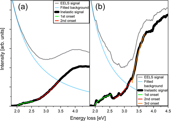
Fig. 7 shows low-loss EELS spectra from the nanocomposite and IDB samples from 1.8 to 4.5 eV. For the nanocomposite, the data was collected directly from a ZnFe2O4 NP extending through the TEM sample. Signal from the ZnO grains nearby was consequently not observed in this spectrum. The spectrum from the IDB sample is a convolution of the signal from ZnO grains and IDBs, which was unavoidable due to inelastic delocalization.37
The EELS results indicate two absorption onsets in the spinel ZnFe2O4 NPs. The first absorption onset occurred at 2.0 eV and represents the absorption band edge. This value is consistent with our DRS data. Another absorption onset was found around 2.6 eV. The two transitions were fitted to the lineshape of a direct and an indirect transition, respectively. The first transition corresponds well with the expected band gap of ZnFe2O4.12,34 Interestingly, the energy of the second transition corresponds approximately with one of the electronic transitions observed in photoluminescence measurements on ZnFe2O4 which Granone et al.,12 attributed to a transition involving Zn. Importantly, the data show that spinel ZnFe2O4 NPs embedded in ZnO have absorption onsets at energies similar to bulk ZnFe2O4. Hence, embedding spinel ZnFe2O4 NPs in a ZnO TCO is a viable approach to enhance absorption in the yellow, green and blue bands of the visible spectrum, while leaving the composite transparent in the red band.
In the EELS spectrum from the IDB sample, we find that the line shape has three contributions: a direct transition at 2.0 eV, an indirect transition at 2.6–2.7 eV, and a direct transition at 3.2 eV. The transition at 3.2 eV is due to band-to-band transitions in ZnO, while the first transition at 2.0 eV is the absorption band edge of the sample. The absorption band edge position is consistent with our DRS data. Both EELS and DRS indicate another transition around 2.6–2.7 eV in the IDB sample.
Generally, for both the nanocomposite and the IDB sample, the onset energies from EELS and DRS are in good agreement. The data clearly reveals similar optical absorption in spinel ZnFe2O4 NPs and Fe-decorated IDBs. Previously, density functional theory (DFT) studies of the band structure of ZnFe2O4 have revealed that the valence band maximum (VBM) and the conduction band minimum (CBM) is mainly made up of Fe 3d and O 2p states,38 so the size of the bandgap is largely determined by the bonding between these elements. As noted above, both the nanocomposite and the IDB sample contain layers of Fe octahedrally coordinated by O. We also found above that the majority of Fe is octahedrally coordinated by O in both samples. Since the DFT results from literature show that the size of the band gap is largely determined by the bonding between Fe and O, it is thus reasonable to conclude that the similar optical absorption in the two samples arises from the structural similarity. Crystallographically, Fe-decorated b-IDBs cannot be accurately described as spinel ZnFe2O4 inclusions in ZnO. However, motivated by the structural and functional similarities described above, we suggest that b-IDBs can be viewed as few-layer spinel-like inclusions in ZnO.
Valence band XPS spectra from all the samples are presented in the ESI.† The data show that the nanocomposite and the IDB sample have valence band maxima at approximately the same energy, and that the valence band XPS spectrum from the nanocomposite can be explained as a combination of ZnO and ZnFe2O4. These observations are consistent with Fe-decorated b-IDBs behaving similarly to spinel ZnFe2O4. Please see the ESI† for a full discussion of the valence band XPS spectra.
With the excellent spatial resolution provided by the low-loss EELS measurements, we have demonstrated that the absorption bands at ∼2.0 and ∼2.6 eV in the nanocomposite originate from the ZnFe2O4 nanoparticles. In the IDB sample, the data do not allow us to conclusively rule out contributions from defects in the ZnO grains to the optical absorption properties. Defects that may contribute include vacancies, intrinsic interstitials, and solute Fe. If the absorption properties of the IDB sample are attributed to defects in the ZnO grains, then the functional similarity between the nanocomposite and the IDB sample is coincidental. However, both samples had absorption onsets at 2.0 and 2.6 eV, so we find that such a coincidence is unlikely. Furthermore, contributions to absorption from defects tend to manifest as an Urbach tail. We have tried to suppress contributions from the Urbach tail to the absorption band edge analysis by applying Tauc plots. Finally, the valence band XPS spectra from the two samples are similar (see the ESI†). This is expected if Fe-decorated b-IDBs behave similarly to spinel ZnFe2O4. From the presented data, the most probable interpretation is therefore that the structural similarity around Fe-ions at b-IDBs and in spinel ZnFe2O4 causes the observed functional similarities.
The DRS data is, in principle, susceptible to contributions from the impurity phase detected in the diffractogram from the IDB sample. However, the superior spatial resolution of EELS, along with simultaneous access to structural data, revealed that the absorption onsets at 2.0 eV and 2.6–2.7 eV cannot be attributed to impurity phases.
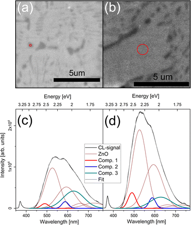
CL spectra in the range from 1.6 to 3.8 eV were collected from all samples at 80 K, see Fig. 8 and 9 for the nanocomposite and IDB sample respectively. Measurements on the bulk ZnO sample revealed the characteristic near-band-edge (NBE) emission of ZnO and a separate broad defect band. The defect band was well described by fitting with 4 Gaussian emission components. Fitting of the bulk ZnFe2O4 emission required 7 Gaussian emission components, centered at 3.0 (B1), 2.6 (B2), 2.3 (B3), 2.2 (B4), 2.1 (B5), 2.0 (B6) and 1.9 (B7) eV. B6 and B7 are likely due to NBE and defects in ZnFe2O4,12,33 respectively. B2 and B3 are consistent with previous reports of luminescence from higher-lying bands in ZnFe2O4.12 See the ESI† for deconvolution of the luminescence from both bulk samples (Fig. S6†).
Fig. 8 shows CL data from the nanocomposite. To deconvolute the spectra, emission components from the bulk ZnO sample were included, and three further components had to be introduced, centered at 2.5, 2.1 and 2.0 eV. The additional peaks at 2.1 and 2.0 eV are close to components B5 and B6 from the bulk ZnFe2O4 sample, but have a different width than those of the bulk sample. In contrast, the peak at 2.5 eV does not match any emission component from the bulk ZnFe2O4 sample. Hence, the luminescence from the nanocomposite could not be deconvoluted as a simple combination of emission components from the ZnO and ZnFe2O4 bulk samples. There are several possible origins for the additional emission peaks. First, there could be luminescence contributions from the ZnO/ZnFe2O4 interfaces, which are not present in either of the bulk samples. Second, the XPS data revealed a non-zero inversion parameter for the nanocomposite. In the literature, some authors have observed a change in luminescence peak positions as a function of the inversion parameter,33 while others have found only changes in peak intensities.12 Finally, solute Fe in ZnO could contribute to the luminescence. This possibility will be discussed below. The intensity of the component at 2.0 eV increased when measuring directly on ZnFe2O4 NPs, and the energy of this emission component agrees with the band gap of ZnFe2O4 as determined from our EELS and DRS data as well as previous reports in the literature.12,34 Therefore, this emission component is likely related to NBE emission in the ZnFe2O4 NPs.
Note that secondary electron (SE) imaging is more surface sensitive than the CL measurements. Consequently, the underlying ZnO matrix can contribute to the CL signal, even when the signal is acquired from an area corresponding to a ZnFe2O4 NP as determined from the SE image.
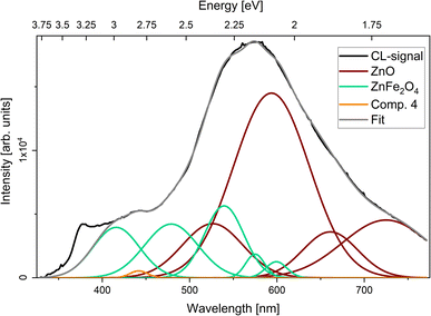
CL measurements on the IDB sample (Fig. 9) featured an increase in luminescence between 2.6 and 3.1 eV compared to the spectra from the bulk ZnO sample. Spectral deconvolution was achieved using emission components from bulk ZnO and bulk ZnFe2O4, keeping both the peak energy and width constant for all components. The spectrum from the IDB featured a final minor emission peak at 2.8 eV, which was accounted for by addition of a final fitting component. The ZnO NBE was not included in the fitting.
The optical properties of solid solutions of Fe in ZnO have not been explicitly studied here, and contributions from Fe dopants cannot be ruled out in the interpretation of our luminescence data. Previous work by Wang et al. has shown a broadening in photoluminescence from ZnO samples doped with Fe in the spectral region between 2.4 and 3.0 eV approximately.39 Hence, solute Fe in ZnO could contribute to the observed luminescence in this range in our CL data. However, the absence of diffraction peaks from ZnO in the bulk ZnFe2O4 sample in the XRD data (see Fig. 1) indicates that if there are ZnO particles in this sample they are either small or make up a small volumetric ratio of the sample. Hence contributions from solute Fe in ZnO are considered unlikely to dominate the luminescence from the bulk ZnFe2O4 sample. Since luminescence components from the bulk ZnFe2O4 sample were used to deconvolute the luminescence from the IDB sample, we therefore argue that luminescence from Fe-decorated IDBs likely contributed to the CL data. It should be noted that alternative deconvolutions may be possible with the large number of luminescence components used for the IDB sample. The luminescence components at 2.5 and 2.1 eV in the nanocomposite could be due to luminescence from solute Fe in ZnO. However, we argue that the emission component at 2.0 eV in the nanocomposite is likely due to NBE emission in the ZnFe2O4 NPs, since its energy matches the expected bandgap of ZnFe2O4, and due to the variation in the intensity of this luminescence component as a function of position on the sample. Further studies are required to unambiguously determine the origin of all emission components.
4 Conclusion
The optical properties of ZnO were modified through incorporation of ZnFe2O4 spinel particles. We have shown that the optical properties are changed through the incorporation of the spinel particles, specifically that the absorption edge is lowered from 3.3 eV for pristine ZnO, to 2.0 eV in samples containing the ZnFe2O4 spinel particles. Furthermore, samples containing Fe-decorated IDBs and samples containing embedded spinel ZnFe2O4 particles displayed similar absorption properties. We suggest that the origin of this similarity is the layers of Fe octahedrally coordinated by O, which is present in both samples. We have demonstrated that by introducing iron into ZnO, the optical band gap of the system can be modified, making iron-containing ZnO a candidate as a modified TCO for improving solar cell efficiency. CL measurements suggest that luminescence from ZnO containing Fe-decorated IDBs is explained by a combination of ZnO and spinel ZnFe2O4 luminescence, whereas increased luminescence near the bandgap of spinel ZnFe2O4 was observed from spinel ZnFe2O4 nanoparticles embedded in ZnO.Author contributions
S. B. Kjeldby: conceptualization; data curation; formal analysis; investigation; methodology; visualization; writing – original draft; writing – review & editing. P. D. Nguyen: conceptualization; data curation; formal analysis; investigation; methodology; supervision; validation; visualization; writing – original draft; writing – review & editing. J. García-Fernández: conceptualization; formal analysis; investigation; methodology; visualization; writing – original draft; writing – review & editing. K. Haug: conceptualization; investigation; methodology. A. Galeckas; formal analysis; investigation; supervision; visualization; writing – review & editing. I. J. T. Jensen; formal analysis; investigation; methodology; writing – review & editing. A. Thogersen; formal analysis; investigation; methodology; visualization; writing – review & editing. L. Vines: conceptualization; funding acquisition; methodology; project administration; resources; supervision; validation; writing – review & editing. Ø. Prytz: conceptualization; funding acquisition; methodology; project administration; resources; supervision; validation; writing – review & editing.Conflicts of interest
The authors have no conflicts to disclose.Acknowledgements
The Research Council of Norway is acknowledged for the support to the Norwegian Micro- and Nano-Fabrication Facility, NorFab (Project No. 295864) and the Norwegian Center for Transmission Electron Microscopy, NORTEM (Project No. 197405) and for support to the project Functionalization of Conducting Oxides by Ion beam and defect engineering (Project No. 287729). The authors would like to thank Ole Bjørn Karlsen for fruitful discussions.References
- V. Srikant and D. R. Clarke, J. Appl. Phys., 1998, 83, 5447 CrossRef CAS.
- M. A. Borysiewicz, Crystals, 2019, 9, 505 CrossRef CAS.
- Ü. Özgür, et al. , J. Appl. Phys., 2005, 98, 041301 CrossRef.
- P. Souletie, et al. , J. Cryst. Growth, 1988, 86, 248 CrossRef CAS.
- W. W. Wenas, et al. , Jpn. J. Appl. Phys., 1991, 30, L441 CrossRef CAS.
- M. C. Beard, et al. , Acc. Chem. Res., 2013, 46, 1252 CrossRef CAS PubMed.
- B. L. Aarseth, et al. , Nanotechnology, 2021, 32, 505707 CrossRef CAS PubMed.
- C. S. Granerød, et al. , Nanotechnology, 2019, 30, 225702 CrossRef PubMed.
- S. B. Kjeldby, et al. , J. Appl. Phys., 2022, 131, 125701 CrossRef CAS.
- S. A. Degterov, et al. , Metall. Mater. Trans. B, 2001, 32, 643 CrossRef.
- S. Zhou, et al. , J. Phys. D: Appl. Phys., 2007, 40, 964 CrossRef CAS.
- L. I. Granone, et al. , Catalysts, 2019, 9, 434 CrossRef CAS.
- I. Almansouri, et al. , IEEE J. Photovoltaics, 2015, 5, 968 Search PubMed.
- A. K. Srivastava, et al. , Mater. Chem. Phys., 2009, 114, 194 CrossRef CAS.
- M. Chandrika, et al. , Mater. Chem. Phys., 2019, 230, 107 CrossRef CAS.
- N. Kislov, et al. , Mater. Sci. Eng. B, 2008, 153, 70 CrossRef CAS.
- R. Bayat, et al. , Solid State Sci., 2019, 89, 167 CrossRef CAS.
- S. D. Kulkarni, et al. , Mater. Res. Bull., 2016, 77, 70 CrossRef CAS.
- N. Daneu, S. Bernik and A. Rečnik, J. Phys.: Conf. Ser., 2011, 326, 012003 CrossRef.
- T. Walther, et al. , Int. J. Mater. Res., 2006, 97, 934 CAS.
- O. Köster-Scherger, et al. , J. Am. Ceram. Soc., 2007, 90, 3984 Search PubMed.
- H. Schmid, E. Okunishi and W. Mader, Ultramicroscopy, 2013, 127, 76 CrossRef CAS PubMed.
- H. Schmid, et al. , Micron, 2012, 43, 49 CrossRef CAS PubMed.
- J. Hoemke, et al. , J. Am. Ceram. Soc., 2017, 100, 4252 CrossRef CAS.
- J. Hoemke, et al. , J. Am. Ceram. Soc., 2018, 101, 2616 CrossRef CAS.
- F. Wolf, B. H. Freitag and W. Mader, Micron, 2007, 38, 549 CrossRef CAS PubMed.
- M. Bosman, et al. , Ultramicroscopy, 2006, 106, 1024 CrossRef CAS PubMed.
- M. Bosman, et al. , Appl. Phys. Lett., 2009, 95, 101110 CrossRef.
- W. Zhan, et al. , Nanotechnology, 2017, 28, 105703 CrossRef CAS PubMed.
- T. Hörlin, G. Svensson and E. Olsson, J. Mater. Chem., 1998, 8, 2465 RSC.
- W. Zhan, et al. , Materials, 2019, 12, 888 CrossRef CAS PubMed.
- T. Yamashita, R. Hansson and P. C. Hayes, J. Mater. Sci., 2006, 41, 5559 CrossRef CAS.
- Y. Li, et al. , Chem. Geol., 2019, 504, 276 CrossRef CAS.
- L. I. Granone, et al. , Phys. Chem. Chem. Phys., 2018, 20, 28267 RSC.
- K. Ismail, et al. , Appl. Phys. Lett., 1991, 58, 1539 CrossRef CAS.
- M. Choi, et al. , Appl. Phys. Lett., 2015, 106, 192902 CrossRef.
- R. F. Egerton, Electron Energy-Loss Spectroscopy in the Electron Microscope, Springer Science & Business Media, 3rd edn, 2011 Search PubMed.
- J. Yao, et al. , Integr. Ferroelectr., 2013, 145, 17 CrossRef CAS.
- Y. S. Wang, P. John Thomas and P. O'Brien, J. Phys. Chem. B, 2006, 110, 21412 CrossRef CAS PubMed.
Footnote |
| † Electronic supplementary information (ESI) available. See DOI: https://doi.org/10.1039/d2na00849a |
| This journal is © The Royal Society of Chemistry 2023 |

