DOI:
10.1039/D2NA00889K
(Paper)
Nanoscale Adv., 2023,
5, 2238-2243
GaN nanowires prepared by Cu-assisted photoelectron-chemical etching
Received
4th December 2022
, Accepted 7th March 2023
First published on 7th March 2023
Abstract
A novel Cu-assisted photoelectron-chemical etching is proposed to fabricate GaN nanowires. The functional mechanism of assisted metals, etchant concentrations, and the addition of H2O2 was investigated based on theoretical analysis and experiments. The low-cost metal-assisted etchant (CuSO4) proved more favorable than the conventional noble one (AgNO3) for the preparation of GaN nanowires in this work. The formed Ag dendrite blocked the etching when adopting the Ag-assisted etchant, while the Cu-assisted one did not. Moreover, the etchant consisting of 0.01 M CuSO4 and 5 M HF was demonstrated to realize a relatively good surface morphology and fast etching rate. In addition, the common oxidant H2O2 introduced a quasi-stable configuration between the Cu deposition and dissolution, slowing down the formation of the GaN nanowires. The proposed Cu-assisted photoelectron-chemical etching with the advantages of low cost, room temperature, and controllability could offer a new way to fabricate GaN nano-devices.
1. Introduction
GaN nanowires are a promising choice to promote novel nanoelectronic and nanophotonic devices due to their unique physicochemical properties such as a wide direct band gap, and superior thermal stability.1–3 However, it remains challenging to prepare GaN nanowires. There are two conventional ways to fabricate GaN nanowires at present. One is the bottom-up method by crystal growth, which can realize high-quality GaN nanowires.4,5 The other one is the top-down method by dry etching, which can precisely control the size of nanowires.6,7 The two methods are both expensive and complicated to some degree.8,9 Thus, wet etching has been demonstrated to have significant potential to realize GaN nanowires owing to the simple experimental operation, low etching-induced damage, and material stress relief.10,11
Currently, metal-assisted chemical wet etching (MACE) has been a terrific and mature method to synthesize Si/GaAs nanowires.12–14 However, the MACE of GaN nanowires is yet to be explored further. There are a few reports on the application of noble metals such as Au, Ag, and Pt in the MACE of GaN nanowires. Nevertheless, the application of cheap metals such as Cu, Fe, and Ni is still absent, which is shown in Table 1. Xuewen Geng et al. fabricated GaN nanowires by one-step metal-assisted photochemical wet etching (MaPEtch) with AgNO3 and HF solutions.15 It is found that the region around the metal is easier to etch. Adel Najar et al. adopted Pt metal to perform two-step metal-assisted photochemical etching and realized the GaN nanowires etching with average lengths of about 35 nm and 10 nm.16,17 Pan GeBo et al. carried out two-step metal-assisted photochemical etching of GaN nanowires using Au nanoparticles.18 The whole MaPEtch reaction process was also revealed by analyzing the formation, transport, and recombination of electron–hole pairs during the etching process.
Table 1 Comparison of different MaPEtch methods
| Etching step |
Assisted metal |
Ref. |
| One step |
Ag(noble metal) |
15
|
| Two step |
Pt(noble metal) |
16 and 17 |
| Two step |
Au(noble metal) |
18
|
|
One step
|
Cu(cheap metal)
|
This work
|
In our previous work, we preliminary investigated the application of cheap metals in preparing GaN nanowires and explained the role of metals.19 Based on that, here, we further studied the function of etching solution type and ratio during the process. Moreover, we revealed the theoretical mechanism and experimental method of Cu-assisted etching, which offers a new choice to prepare GaN nanowires.
2. Experimental
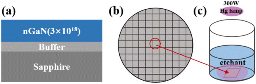
The 3 μm thick Si-doped GaN (0001) films with a carrier concentration of 3.0 × 1018 cm−3 were grown on a 2-inch sapphire substrate by metal–organic chemical vapor deposition (MOCVD) in the experiment. The layer structure is presented in Fig. 1(a).
 |
| | Fig. 1 Schematic diagram of (a) the structure of the GaN sample, (b) the cleaved 2-inch GaN wafer, (c) the experimental setup. | |
2.1 Wafer cleaning
The 2-inch GaN wafer was cleaved into 1 cm2 squares, as shown in Fig. 1(b). The standard RCA cleaning process was applied to clean the chips. Then, the chips were rinsed in deionized water (DI water) for 10 min. After that, the chips were immersed in acetone, ethanol, and DI water for 10 min, respectively. Finally, the chips were dried using N2.
2.2 Synthesis of GaN nanowire
In this step, the GaN chips were soaked in etchants to synthesize GaN nanowires by the MACE process. The diagram of the experimental setup is shown in Fig. 1(c). The etchants consisted of HF and CuSO4 or AgNO3 for a comparison. In addition, the common oxidant, H2O2 was also applied. The proportion of etchant was chosen based on the reference and our previous experiments.19–21 The etching process was performed at room temperature under 300 W UV illumination from a Hg lamp. After the MACE process, GaN chips were treated with a concentrated HNO3 solution for 30 min to remove the residual metal NPs. The etched nGaN chips were then rinsed thoroughly in DI water and dried with N2. The morphologies of the etched chips in plan-view and cross-section were characterized using scanning electron microscopy (SEM). Furthermore, Raman spectroscopy with a 632.8 nm exciting source was performed to identify the optical properties.
3. Results and discussion
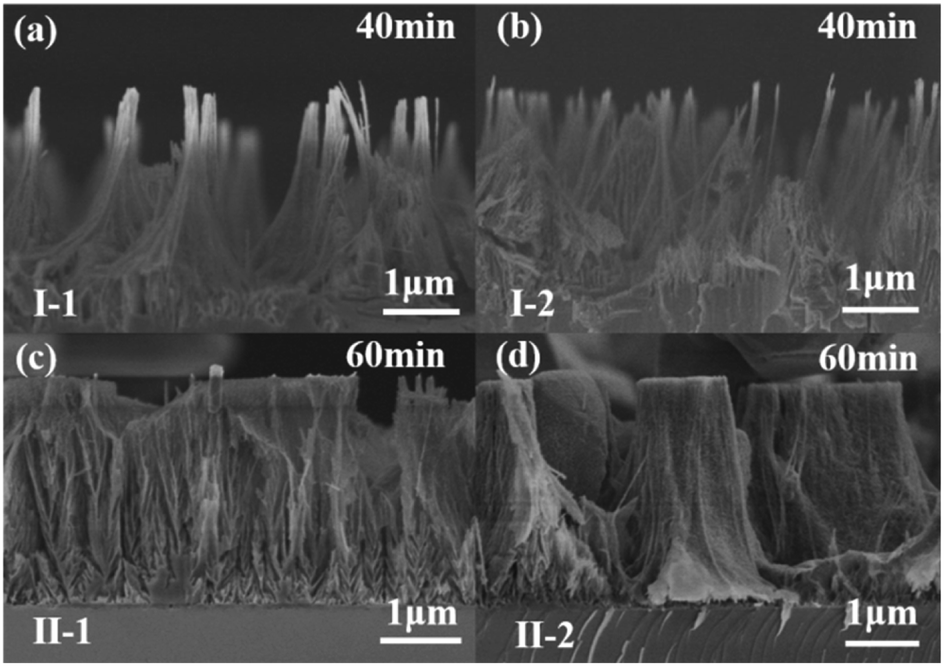
3.1 Comparison between Cu-etchants and Ag-etchants
Two kinds of etching conditions were used to prepare GaN nanowires in our experiments, as listed in Table 2. The I-type experiments applied CuSO4 and HF as the etchant (Cu-etchant), while the II-type ones applied AgNO3 and HF as the etchant (Ag-etchant). We adopted 10 mM CuSO4/2.5 M HF, 10 mM CuSO4/5 M HF, 10 mM AgNO3/5 M HF, and 20 mM AgNO3/5 M HF for comparative experiments.
Table 2 Etching conditions for Cu-etchants and Ag-etchants
| Experiments |
[CuSO4] (mM) |
[AgNO3] (mM) |
[HF] (M) |
Etching time (min) |
| I-1 |
10 |
|
2.5 |
40 |
| I-2 |
10 |
|
5 |
40 |
| II-1 |
|
10 |
5 |
60 |
| II-2 |
|
20 |
5 |
60 |
Fig. 2 shows the etching results under conditions I-1, I-2, II-1, and II-2. With Cu-etchant, the nanowires will significantly reduce once a longer etching time than 40 min is applied, while with Ag-etchant, 40 min etching time is not enough to obtain the typical uniform nanowires. A longer etching time than 60 min also made no apparent difference in the etching results. Thus, to achieve the observable nanowires, 40 min was adopted to etch with Cu-etchant and 60 min with Ag-etchant, respectively. As shown in Fig. 2(a) and (b), uniform and structured GaN nanowires were obtained with the etchants consisting of CuSO4 and HF after 40 min of etching under conditions I-1 and I-2, respectively. However, as shown in Fig. 2(c) and (d), only a small number of GaN nanowires were fabricated, and there were a large number of GaN nanopores after 60 min of etching under the conditions II-1 and II-2, respectively. Although the morphological changes in Fig. 2(d) are similar to those in Fig. 2(c), the increase of AgNO3 concentration from 0.01 M to 0.02 M gave rise to more columnar aggregation as shown in Fig. 2(d). The main reason is the separation of electron–hole pairs driven by the UV light, which will be blocked by the formed Ag dendrites on the surface of GaN. Then, the etching ended and column structures were formed. By comparing and analyzing the results of two kinds of etchants, it was demonstrated that Cu-etchant is more suitable to prepare regular GaN nanowires than Ag-etchant to some degree. So, further studies on the functions and mechanism of Cu-etchant in GaN nanowires MACE were carried out.
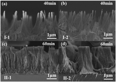 |
| | Fig. 2 Cross-sectional SEM image of GaN nanowires for (a) experiment I-1, 40 min, (b) experiment I-2, 40 min, (c) experiment II-1, 60 min, (d) experiment II-2, 60 min. | |
3.2 GaN nanowires synthesized through Cu-ACE
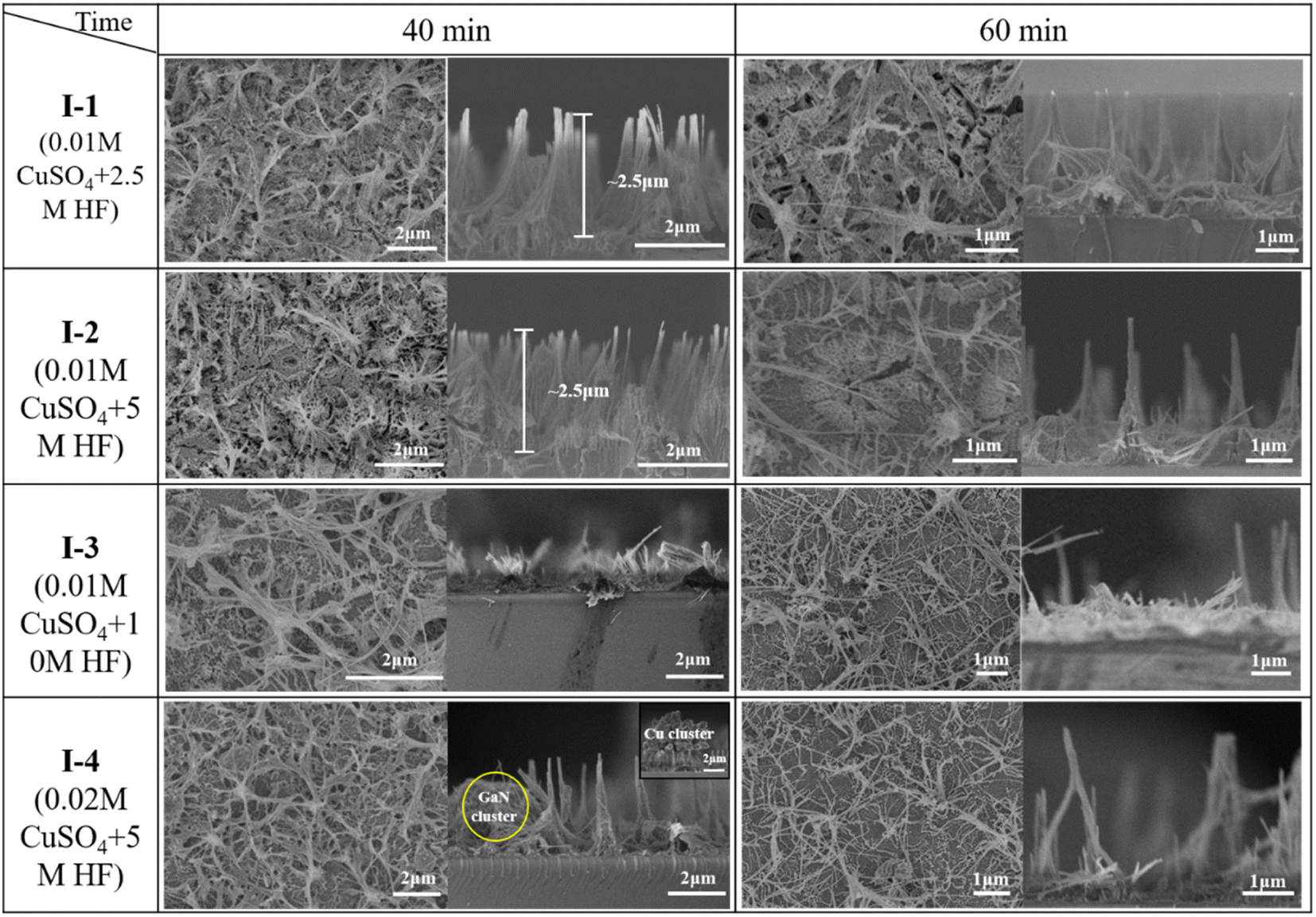
Typical GaN nanostructures were obtained using Cu-etchant with different concentrations. As shown in Table 3, different Cu-etchants were adopted in our experiments (defined as experiments I-1, I-2, I-3, I-4, and I-5). The SEM images for etched morphologies are described in Fig. 3, 5 and 6.
Table 3 Summary of etching conditions for Cu-etchants
| Experiments |
[CuSO4] (mM) |
[HF] (M) |
[H2O2] (M) |
Etching time (min) |
| I-1 |
10 |
2.5 |
|
40, 60 |
| I-2 |
10 |
5 |
|
20–60 |
| I-3 |
10 |
10 |
|
40, 60 |
| I-4 |
20 |
5 |
|
40, 60 |
| I-5 |
10 |
2.5 |
0.6 |
30, 60, 120 |
 |
| | Fig. 3 Cross-sectional and plan-view (the inset) SEM image of GaN nanowires under condition I-2 for (a) 20 min, (b) 30 min, (c) 40 min, (d) 50 min. | |
To extract more comprehensive and reliable information on the nanowire morphology under condition I-2, the GaN thin films were cleaved and examined by cross-sectional SEM. Fig. 3 shows the cross-sectional images of the as-grown GaN thin film and nGaN thin films etched at different etching durations. After etching for 20 min, the etched GaN-20 showed a wire structure (Fig. 3(a)). The etching depth was about 1 μm, and the average diameter of the nanowires was about 70 nm. The inset is the SEM of the chip surface, and the highlighted area corresponds to the top of clustered nanowires. After 30 min of etching, the wires became finer, and the etching depth was about 1.3 μm. The average diameter of the nanowires was about 20 nm, which can be seen from the inset in Fig. 3(b). After 40 min of etching, the etching depth was about 2.2 μm, and the average diameter of the nanowires was about 20 nm. As seen in the inset of Fig. 3(c), the nanowire clusters were obviously reduced, and the holes at the bottom were clear. After 50 min of etching, the etching depth was about 3 μm, and the average diameter of the nanowires was about 20 nm. The inset in Fig. 3(d) shows that the nanowires were etched to the bottom. The average diameter of the nanowires is about 20 nm. Moreover, nanowires disappeared in one part of the area and accumulated in another part. In summary, as the etching proceeded, the GaN nanowires became thinner, and the etching depth gradually increased. An etching depth of 3 μm corresponds to an etching rate of 60 nm min−1 for the GaN nanowires.
Fig. 4 shows the Raman spectra of the unetched and etched GaN. According to the Raman scattering analysis, the E2 phonon frequency for the strain-free bulk hexagonal GaN grown on Si was 567.5 cm−1. The E2 phonon frequency of GaN was impacted by just stress. As shown in Fig. 4, the unetched GaN was under tensile stress. The E2 phonon frequency for GaN nanowires was also 567.5 cm−1. An increase of E2 phonon frequency after etching 50 min with respect to strained-free GaN indicated the relaxation of tensile stress. With the increased etching time, the E2 phonon frequency presented a blue shift at the beginning. It turned to a red shift after etching for 20 min. This indicated that the tensile stress increased at first and then decreased. Finally, the stress was completely released. The principle is explained as follows. The uncorroded GaN material mainly decides the Raman spectrum, because only a very thin layer of GaN was etched at the beginning of the reaction. As the etching time increases, GaN nanowires are building up in which the increasing vertical porosity led to tensile stress relaxation.
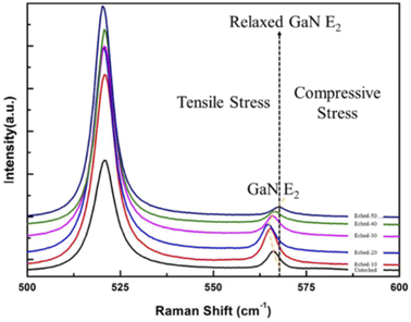 |
| | Fig. 4 Raman spectra of the unetched and etched GaN. | |
The effect of [HF].
Fig. 5 shows the SEM images of GaN nanowires under 40 min/60 min etching with the etchants containing 0.01 M [Cu2+] + 2.5 M [HF](I-1), 0.01 M [Cu2+] + 5 M [HF](I-2), 0.01 M [Cu2+] + 10 M [HF](I-3), and 0.02 M [Cu2+] + 5 M [HF](I-4). Comparing the etching results under conditions I-1 and I-2 after 40 min of etching, it can be seen that the nanostructured layers are both about 2.2 μm thick. It demonstrates that the etching rate is basically constant with the increased HF concentration. But the [HF] increasing from 2.5 M to 5 M led to thinner nanowires. When the HF concentration went up to 10 M (condition I-3), most GaN nanowires were etched away. Part of the nanowires began to collapse and lay flat on the surface of GaN. After 60 min of etching under conditions I-1, I-2, and I-3, the number of nanowires gradually decreased as the GaN was etched to the bottom. Moreover, higher [HF] etched away more nanowires. The 10 M [HF] almost consumed all the GaN nanowires. In summary, the concentration of HF is one of the key factors of the lateral etch rate. With the same etching time, the etching depths showed little difference as the [HF] increased from 2.5 M to 10 M. But the nanowires gradually became thin to collapse and disappear. Thus, to prepare uniform GaN nanowires, the HF concentration is critical. 5 M is a suitable choice for this experiment.
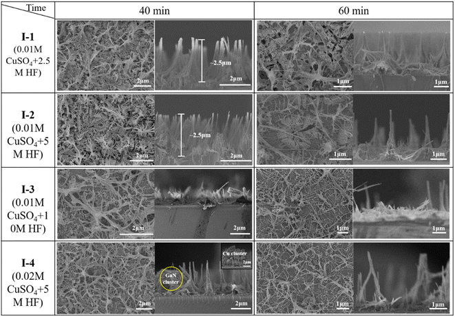 |
| | Fig. 5 Cross-sectional and plan-view SEM image of GaN etching for different conditions. | |
The effect of the [Cu2+].
Comparing the SEM images under conditions I-2 and I-4 after 40 min of etching, it can be seen that the depth of the nanostructured layers increased from about 2.2 μm to 3 μm. It demonstrated that the etching rate was improved with the increase of Cu2+ concentration. The diameters of the GaN nanowires showed little difference. Moreover, when the [Cu2+] increased from 0.01 M to 0.02 M, a part of GaN was not etched into nanowires, which is marked by a yellow circle in Fig. 5. It is probably because the increase of [Cu2+] causes the Cu particles to accumulate faster, which blocks the UV light and results in partially stopping the GaN etching.22 After etching for 60 min under conditions I-2 and I-4, the number of nanowires decreases as the GaN was etched to the bottom. In general, it demonstrates that the [Cu2+] played an important catalytic role in the process and is related to the vertical etching rate. Although the vertical etching rate increased as the [Cu2+] increased from 0.01 M to 0.02 M, the GaN nanowires presented nonuniformity. 0.01 M [Cu2+] is a suitable choice in this experiment.
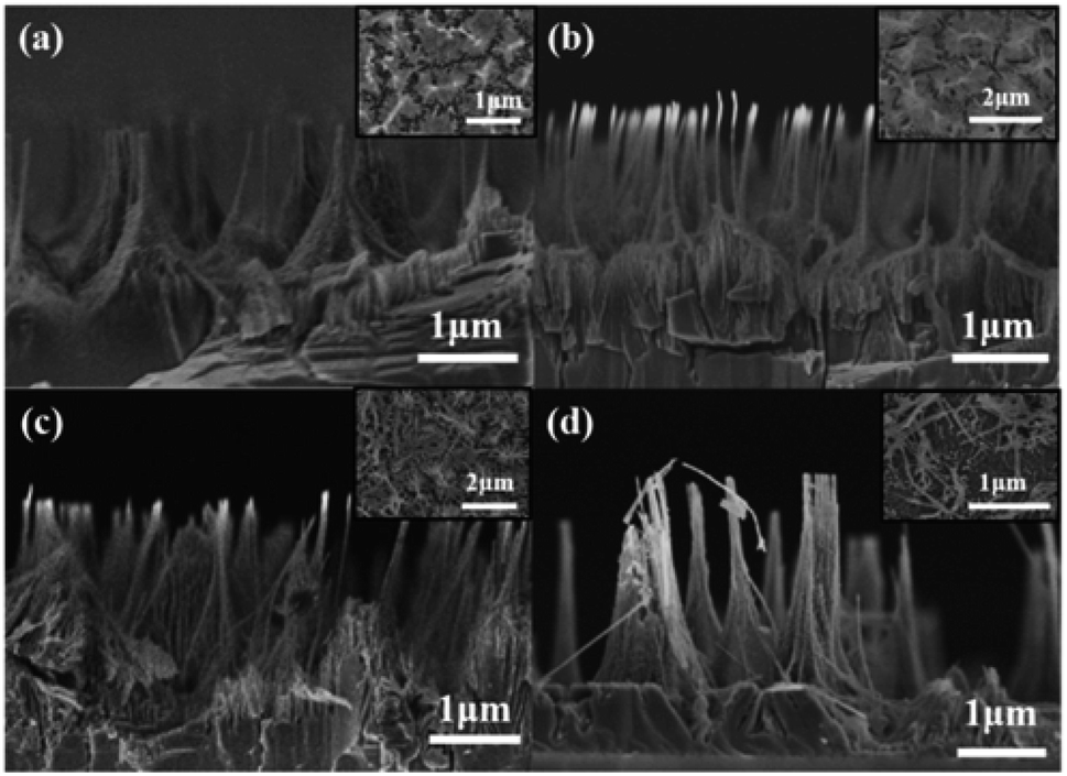
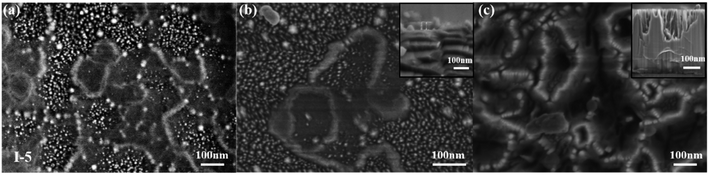
The effect of the [H2O2].
[H2O2] is a common and essential oxidant in MacEtch.23 To verify the role of H2O2 in this proposed GaN MacEtch, the comparative experiment was carried out with I-5 (0.01 M [Cu2+] + 2.5 M [HF] + 0.6 M [H2O2]). Fig. 6 shows the SEM images of GaN nanopores treated with I-5 after 30 min/60 min/120 min of etching. As shown in Fig. 6(a), the surface of GaN-30 becomes porous after 30 min of etching. As can be seen in Fig. 6(b), after 60 min of etching, the surface of GaN-60 remains porous, and the etching depth was about 50 nm, which is presented by the section view in the inset. Fig. 6(c) shows that the surface of GaN-120 remains porous after 120 min of etching. But the diameters of pores enlarge. The section view in the inset of Fig. 6(c) presents the etching depth as about 120 nm, and the etching depth varies. This experiment demonstrates that the addition of H2O2 slows down the etching reaction and blocks the formation of nanowires.
 |
| | Fig. 6 Cross-sectional and plan-view (the inset) SEM image of GaN nanostructures under condition I-5 for (a) 30 min, (b) 60 min, (c) 120 min. | |
3.3 Mechanisms on GaN etching
According to the ref. 24 and 25, the MACE substantially belongs to anodic etching, which could be considered as two concurrent processes. One is the formation of porous GaN, and the other is the electropolishing of GaN. The two processes are highly related to electron–hole generation and transport. In our proposed MACE process, a pair of redox reactions at the cathode (GaN–liquid interface) and anode (Cu–GaN) interfaces could be expressed as:
Cathode:
Anode:
| | | 2GaN + 6h+ → 2Ga3+ + N2↑ | (2) |
| | | Ga3+ + xHF → GaFx3−x + xH+ | (3) |
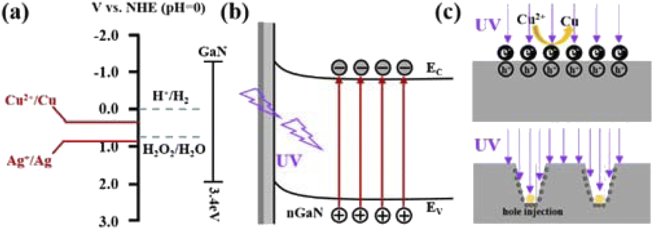
As shown in Fig. 7(a), electron–hole pairs are difficult to separate because of the wide bandgap of GaN. The UV light was adopted to separate the electron–hole pairs, as shown in Fig. 7(b). It can be seen from Fig. 7(c), the galvanic displacement between Cu2+ ions and GaN occurs, leading to the Cu nanoclusters growing on GaN surfaces. The nucleation of Cu nanoclusters was realized by withdrawing the electrons from GaN, while the GaN contacted with Cu2+ ions was oxidized. Consequently, GaN was locally oxidized and dissolved by HF. The dissolving reaction is explained using formulas (2) and (3). The Cu particles sink into the formed channel. The channels form because the current density under the Cu particles is high enough to electropolish (regime A: tetravalent dissolution) and GaN is largely etched away. As the reaction went on, the current density decreased due to the increasing distance between the particles and GaN. Then GaN was locally removed, and the pGaN walls were formed (regime B: divalent dissolution), as shown in Fig. 7(c).
 |
| | Fig. 7 (a) Qualitative diagram of a comparison between the electrochemical electron energy levels of GaN band edges (Ec and Ev are the conduction and valence band energies, respectively) and Cu2+/Cu, Ag+/Ag, H2O2/H2O in HF solution, (b) GaN electron–hole pairs were generated under UV illumination, (c) commonly adopted model of MACE with isolated metal particles. In the presence of the CuSO4/HF solution the particles catalyze the ablation of GaN leading to the formation of cylindrical channels in the substrate. | |
The influence of H2O2.
The experiment demonstrates that H2O2 slows down the etching and is unfavorable for the formation of the nanowires. This is because the addition of H2O2 introduces the dissolution reaction of Cu, given by the formula:| | | Cu + H2O2 + 2H+ → 2H2O + Cu2+ | (4) |
Formulas (1) and (4) show the competition of Cu dissolution against the reduction of Cu2+ ions. Thus, adding H2O2 gives rise to a quasi-stable configuration between the Cu deposition and dissolution. This results in the decrease of Cu deposition and further decreases the GaN etching rate. As such, the addition of H2O2 will block GaN etching and the formation of GaN nanowires.
4. Conclusions
In summary, we developed a Cu-assisted photoelectron-chemical etching method to fabricate GaN nanowires. The function of assisted metals, etchant concentrations, and the addition of H2O2 was investigated by experiments and theoretical analysis. The adopted CuSO4 was demonstrated to be more favorable than AgNO3 on GaN nanowire preparations, which proved the advantages of cheap metal-assisted etching. The etchant consisting of 0.01 M CuSO4 and 5 M HF could realize GaN nanowires with a higher etching rate and better morphology. The addition of H2O2 is unfavorable for the preparation of GaN nanowires because the quasi-stable configuration between the Cu deposition and dissolution was introduced. We propose and demonstrate a cost-effective, room-temperature, and controllable Cu-assisted photoelectron-chemical etching to prepare GaN nanowires, which could promote the fabrication of novel GaN nano-devices.
Conflicts of interest
There are no conflicts to declare.
Acknowledgements
This work was supported by the Technology Innovation and Application Demonstration Key Project of Chongqing Municipality (cstc2020jscx-gksbX0011), the Science and Technology Research Program of Chongqing Municipal Education Commission (KJQN202100614), the Natural Science Foundation of Chongqing (cstc2021jcyj-bshX0146), the Technology Innovation and Application Demonstration Key Project of Chongqing Municipality (cstc2019jszx-zdztzxX0005).
Notes and references
- M. A. Johar, T. Kim, H.-G. Song, A. Waseem, J.-H. Kang, M. A. Hassan, I. V. Bagal, Y.-H. Cho and S.-W. Ryu, Nanoscale Adv., 2020, 2, 1654–1665 RSC.
- Z. Xing, Y. Zhao, L. Bian, J. Zhang, M. Zhou, W. Yang, Y. Wu, M. Jiang, J. Long and S. Lu, Mater. Adv., 2021, 2, 1006–1015 RSC.
- M. Kraut, F. Pantle, J. Winnerl, M. Hetzl, F. Eckmann, I. D. Sharp and M. Stutzmann, Nanoscale, 2019, 11, 7967–7975 RSC.
- S. Sankaranarayanan, P. Kandasamy and B. Krishnan, ACS Omega, 2019, 4, 14772–14779 CrossRef CAS PubMed.
- P. Blanchard, M. Brubaker, T. Harvey, A. Roshko, N. Sanford, J. Weber and K. Bertness, Crystals, 2018, 8, 178 CrossRef.
- M. F. Fatahilah, F. Yu, K. Strempel, F. Romer, D. Maradan, M. Meneghini, A. Bakin, F. Hohls, H. W. Schumacher, B. Witzigmann, A. Waag and H. S. Wasisto, Sci. Rep., 2019, 9, 10301 CrossRef PubMed.
- S. Fernández-Garrido, T. Auzelle, J. Lähnemann, K. Wimmer, A. Tahraoui and O. Brandt, Nanoscale Adv., 2019, 1, 1893–1900 RSC.
- J. Lohani, S. Varshney, D. S. Rawal, S. Sapra and R. Tyagi, Nano-Struct. Nano-Objects, 2019, 18, 100284 CrossRef CAS.
- M. Shimauchi, K. Miwa, M. Toguchi, T. Sato and J. Motohisa, Appl. Phys. Express, 2021, 14, 111003 CrossRef CAS.
- V. V. Lendyashova, K. P. Kotlyar, R. R. Reznik, T. N. Berezovskaya, E. V. Nikitina, I. P. Soshnikov and G. E. Cirlin, J. Phys.: Conf. Ser., 2020, 1695, 012047 CrossRef CAS.
- A. K. K. Soopy, Z. Li, T. Tang, J. Sun, B. Xu, C. Zhao and A. Najar, Nanomaterials, 2021, 11, 126 CrossRef CAS PubMed.
- Z. Huang, N. Geyer, P. Werner, J. de Boor and U. Gosele, Adv. Mater., 2011, 23, 285–308 CrossRef CAS PubMed.
- L. Kong, Y. Zhao, B. Dasgupta, Y. Ren, K. Hippalgaonkar, X. Li, W. K. Chim and S. Y. Chiam, ACS Appl. Mater. Interfaces, 2017, 9, 20981–20990 CrossRef CAS PubMed.
- F. Toor, J. B. Miller, L. M. Davidson, W. Duan, M. P. Jura, J. Yim, J. Forziati and M. R. Black, Nanoscale, 2016, 8, 15448–15466 RSC.
- X. Geng, B. K. Duan, D. A. Grismer, L. Zhao and P. W. Bohn, Electrochem. Commun., 2012, 19, 39–42 CrossRef CAS.
- A. Najar and M. Jouiad, Sol. Energy Mater. Sol. Cells, 2018, 180, 243–246 CrossRef CAS.
- S. Assa Aravindh, B. Xin, S. Mitra, I. S. Roqan and A. Najar, Results Phys., 2020, 19, 103428 CrossRef.
- M. R. Zhang, Q. M. Jiang, S. H. Zhang, Z. G. Wang, F. Hou and G. B. Pan, Appl. Surf. Sci., 2017, 422, 216–220 CrossRef CAS.
- Q. Wang, G. Yuan, S. Zhao, W. Liu, Z. Liu, J. Wang and J. Li, Electrochem. Commun., 2019, 103, 66–71 CrossRef CAS.
- Y. Qu, H. Zhou and X. Duan, Nanoscale, 2011, 3, 4060–4068 RSC.
- X. Li, Y. Xiao, C. Yan, K. Zhou, P.-T. Miclea, S. Meyer, S. L. Schweizer, A. Sprafke, J.-H. Lee and R. B. Wehrspohn, Electrochim. Acta, 2014, 138, 476–480 CrossRef CAS.
- Q. Wang, K. Zhou, S. Zhao, W. Yang, H. Zhang, W. Yan, Y. Huang and G. Yuan, Nanomaterials, 2021, 11, 3179 CrossRef CAS PubMed.
- N. Geyer, B. Fuhrmann, H. S. Leipner and P. Werner, ACS Appl. Mater. Interfaces, 2013, 5, 4302–4308 CrossRef CAS PubMed.
- Y. Z. Yong Cao, F. Liu, Y. Zhou, Y. Zhang, Y. Liu and Y. Guo, ECS J. Solid State Sci. Technol., 2015, 4, 331–336 CrossRef.
- W.-J. Tseng, D. H. v. Dorp, R. R. Lieten, P. M. Vereecken and G. Borghs, J. Phys. Chem. C, 2014, 118, 29492–29498 CrossRef CAS.
|
| This journal is © The Royal Society of Chemistry 2023 |
Click here to see how this site uses Cookies. View our privacy policy here. 
 Open Access Article
 This Open Access Article is licensed under a Creative Commons Attribution-Non Commercial 3.0 Unported Licence
 *a,
Wen
Yang
a,
Sheng
Gao
a,
Weizhong
Chen
a,
Xiaosheng
Tang
a,
Hongsheng
Zhang
a,
Bin
Liu
b,
Genquan
Han
c and
Yi
Huang
*a
*a,
Wen
Yang
a,
Sheng
Gao
a,
Weizhong
Chen
a,
Xiaosheng
Tang
a,
Hongsheng
Zhang
a,
Bin
Liu
b,
Genquan
Han
c and
Yi
Huang
*a