
 Open Access Article
 This Open Access Article is licensed under a
 Creative Commons Attribution 3.0 Unported Licence
Structured hybrid photodetectors using confined conducting polymer nanochannels†
Sukanya
Das
 ,
K. H.
Girish
,
N.
Ganesh
and
K. S.
Narayan
*
,
K. H.
Girish
,
N.
Ganesh
and
K. S.
Narayan
*
Chemistry and Physics of Materials Unit, School of Advanced Materials, Jawaharlal Nehru Centre for Advanced Scientific Research, Bengaluru – 560064, India. E-mail: narayan@jncasr.ac.in
First published on 18th October 2023
Abstract
We design and fabricate hybrid organic inorganic perovskite photodetectors that utilize hole transport layer poly(3,4-ethylene dioxythiophene):poly (styrenesulfonate) PEDOT:PSS confined in alumina nanocylinders. This structural asymmetry in the device where the alumina nanopore template is partially filled with PEDOT:PSS provides features that improve certain device characteristics. The leakage component of the current in such devices is considerably suppressed, resulting in enhanced responsivity and detectivity. The funneling aspect of the photogenerated charge carrier transit ultimately leads to fast detectors as compared to conventional perovskite detectors.
1 Introduction
Hybrid perovskite-based photodetectors hold tremendous promise for broadband optoelectronic applications due to the large optical absorption coefficient over the ultraviolet to infrared spectral range and long diffusion lengths. There has been a significant effort to understand the source of hysteresis in current–voltage response, grain boundaries, type of charge defects and ionic migration. The improved understanding of the physics and chemistry of the transport mechanisms in perovskites has led to rapid enhancement of the device performances with striking progress.1–11 Traditional photodetectors that convert optical signals to electrical signals are primarily based on InGaAs, GaN, and Si that require elaborate film growth techniques.12–21 More recently solution processible semiconductor-based hybrid perovskites and organic polymers have shown promise in applications like optical communications, imaging, chemical and biological sensing. However, direct gap solution processible semiconductors with reduced complexity in manufacturing, flexible form factors accompanied by high absorption and carrier lifetime are always desirable over disordered materials in these applications.22–25A photodetector device architecture that incorporates a patterned alumina layer provides robust features that considerably reduce parasitic currents while enhancing the performance parameters. A key ingredient in the device is the nanoconfined PEDOT:PSS with significant electrical conductance along the nanochannels aligning with the transport of the photogenerated carriers. The cylinder walls of nanochannels provide an inherent boundary to the otherwise exposed thin-film junction of the PEDOT-perovskite layer. This integrity of the device structure ensures minimum pinhole formation. Since the HTL in the inverted devices is the first polymer layer on which the light is initially incident, it plays an important role in the device performance and requires good light transmission, energy level alignment and charge transport properties.26,27 The growth of perovskite films, grain sizes and defect density depend also on the interfacial surface properties of the HTL. Nanoconfined perovskites have been utilized in earlier studies25,28,29 which have shown promising device properties and improved stability. There are many stable HTL materials,30–32viz., PTAA, NiOx, CuI and CuSCN which have been studied to date, but PEDOT:PSS remains as one of the best candidates owing to its excellent light transmittance, wettability for perovskite precursors and conductivity of charge carriers.33–35 Parallelly, the low work function ∼5.2 eV, insulating counterpart PSS and high acidity are a few drawbacks of PEDOT:PSS. The hygroscopic nature of PEDOT:PSS also accelerates the perovskite degradation. There have been many studies on the efforts to modify PEDOT:PSS as the HTL in terms of reduction of the hole injection barrier, conductivity enhancement or interfacial surface roughness.36,37 PEDOT:PSS extracts the photogenerated exciton-separated holes through the HTL and perovskite interface and transfers them to the respective electrode. Thus, the modification of the HTL is one of the crucial factors for the enhanced performance of the photodetectors. The structural asymmetry of the PEDOT:PSS/perovskite device also mitigates the ion accumulation at the interface of the HTL/active layer to ensure enhanced device performances.
With the advent of mixed cation and mixed anion perovskites, researchers have achieved better stability, reproducibility and higher yields.28,38 It has been observed that formamidinium lead triiodide, FAPbI3, shows better stability than methylammonium lead triiodide, MAPbI3 perovskite, but this comes along with an undesired photo-inactive yellow δ-FAPbI3 phase. The yellow phase is then prevented by combining MAPbBr3 and FAPbI3. Further, the addition of small cesium cations assists α-FAPbI3 black phase crystallization and has opened a class of materials FA1−xCsxPb(I1−yBry)3 that shows improved thermal and moisture stability with no undesired phase transition within the operating ranges of temperature.39–47 The ease of controlling the stoichiometry and the I/Br and FA/Cs ratios in mixed perovskites help to tune the bandgap of the materials. The required cesium content is dependent on the device processing conditions.48,49 An optimized formula FA0.95Cs0.05Pb(I0.83Br0.17)3 (FACs) has been adopted in the present work in fabricating a vertical HOIP photodetector.
The morphology, conductivity, crystallinity and degree of order in PEDOT-derivatives as a function of structural confinement have been found to be strongly dependent on transport dynamics in our previous studies.50–52 Our understanding of the enhancement in surface and electronic properties of PEDOT derivatives has been employed in fabricating a HOIP photodetector device in this work. The commercial PEDOT:PSS usually comes in different grades with different PSS ratios which effectively shows different work functions, viscosity, conductivity and so on. In this work, we have used a mix of two grades AI4083 and PH1000 which have shown higher magnitudes of photocurrent as compared to an untreated PEDOT:PSS as a HTL. A 50–60 nm thick PEDOT layer is introduced in alumina scaffolds of thickness of around 200 nm with a channel diameter of 20 nm. The remaining length of nanochannels is occupied by the perovskite layer along with a bulk layer (∼300 nm) above the nanochannels. The devices without alumina are analysed as control devices. In this paper, we have studied the enhanced photodetection properties due to the introduction of structural confinement of the HTL along with a portion of the perovskite layer. We have compared the nanochannel device with that of the control device without the alumina in terms of responsivity, EQE, detectivity and response speed.
2 Materials
Device fabrication of the HOIP involved the use of Indium tin oxide (ITO) as the bottom electrode with a 7 Ω □−1 specific sheet resistance and shaped in a particular mask as shown in ESI S1.† PEDOT:PSS is used as a hole transport layer where two grades of polymer have been used, viz., AI4083 and PH1000 with PEDOT/PSS ratios as 1![[thin space (1/6-em)]](https://www.rsc.org/images/entities/char_2009.gif) :6 and 1:2.5, respectively. Formamidinium iodide >99.99% (FAI) from Greatcell Solar, cesium iodide 99.999% (metals basis) (CsI) from Alfa Aesar, 99.99%, trace metals basis lead iodide (PbI2) from Tokyo Chemical Industry and 99.999% (metals basis) lead bromide (PbBr2) from Thermo Fisher Scientific have been used for the preparation of perovskite solution. 99.8% anhydrous N,N-dimethylformamide (DMF), ≥99.9% dimethyl sulfoxide (DMSO) and anhydrous anisole, 99.7% were purchased from Sigma-Aldrich. Phenethylammonium iodide (PEAI) from Greatcell Solar, [6,6]-phenyl-C61-butyric acid methyl ester (PC61BM) and bathocuproine (BCP) from Luminescence Technology Corp. were used.
:6 and 1:2.5, respectively. Formamidinium iodide >99.99% (FAI) from Greatcell Solar, cesium iodide 99.999% (metals basis) (CsI) from Alfa Aesar, 99.99%, trace metals basis lead iodide (PbI2) from Tokyo Chemical Industry and 99.999% (metals basis) lead bromide (PbBr2) from Thermo Fisher Scientific have been used for the preparation of perovskite solution. 99.8% anhydrous N,N-dimethylformamide (DMF), ≥99.9% dimethyl sulfoxide (DMSO) and anhydrous anisole, 99.7% were purchased from Sigma-Aldrich. Phenethylammonium iodide (PEAI) from Greatcell Solar, [6,6]-phenyl-C61-butyric acid methyl ester (PC61BM) and bathocuproine (BCP) from Luminescence Technology Corp. were used.
2.1. Sample preparation
HOIP nanochannel films: 2.5*2.5 cm2 ITO substrates etched in a specific pattern have been used as transparent bottom electrodes for the inverted structure. Standard cleaning processes are adapted by subsequent ultrasonic washing with acetone, isopropyl alcohol, and deionized water. Cleaned substrates are made hydrophilic using RCA, i.e., ammonia:hydrogen peroxide:water (1:1:5 mixture) and air plasma treatment. PMMA-supported AAO membranes are adhered to the ITO substrates with a stepwise acetone bath. The ITO/AAO samples are once again plasma treated. Two grades of PEDOT:PSS, AI4083 and PH1000 are mixed in a 1:1 ratio and stirred for 2–3 h. This solution will be named PEDOT:PSS mix' in the remaining part of the manuscript. The solution is filtered using 0.45 μm PVDF disposable filter paper and spin coated on cleaned ITO/AAO substrates at 4000 rpm for 60 s and 10 s of ramping. The films are then heated at 140 °C for long hours to remove aqueous solvent from the nanochannels. The films are cooled to room temperature before spin coating the perovskite layer inside a nitrogen glovebox. 1 M solution of FA0.83Cs0.17Pb(I0.9Br0.1)3 is prepared by mixing 783.7 mg of PbI2, 285.46 mg of FAI, 110.1 mg of PbBr2 and 88.34 mg of CsI in 2 ml of 4:1 ratio of DMF:DMSO solvent. The solution is stirred for 15 min at 500–600 rpm at 70 °C followed by further stirring overnight without heating. This solution is drop-cast on PEDOT:PSS/AAO substrates and given a waiting time of 40 s before spin coating at 1000 rpm for 10 s followed by 6000 rpm for 35 s. In the last 15 s of spinning, antisolvent anisole is added to the substrates. After spin coating, the films are then immediately transferred to a preheated surface of a heater at 100 °C for 1 h. Slow flushing of the glovebox for 15 min is performed after the annealing is completed to remove any residual vapour of DMF and DMSO. The passivation layer PEAI is then spin coated at 5000 rpm for 30 s and 2500 rpm ramping and kept under ambient conditions in a glovebox for 1–2 min. PC61BM, which is the electron transport layer, is spin coated at 2000 rpm for 30 s and stored inside a glovebox in a covered Petri dish for overnight solvent annealing. Next, the films are heated at 100 °C for 30 min. BCP solution is coated at 4000 rpm for 30 s and heated at 100 °C for 1–2 min. The substrates are allowed to cool to room temp and transferred to a metal mask for Ag electrode deposition. Effectively, 120 nm of Ag is coated following a deposition rate of 0.1 Å s−1 inside the physical vapour deposition chamber. A similar process was followed for control devices without the AAO membranes.
3 Methods
A Keithley 2400 source meter and 532 nm continuous laser were used to study the light and dark photocurrent with variable sizes of the Cu mask on devices and laser intensity dependence. The photocurrent due to different incident wavelengths was analyzed by using grating with a xenon lamp source and a lock-in amplifier. Two probe conductivity measurements were performed using a Keithley Parameter Analyzer 4200SCS. The thickness of the HTL, active layer and ETL was measured using a 300 kHz tip in noncontact mode atomic force microscopy. The lifetime measurements were performed using a YSL photonics supercontinuum laser source. Scanning electron microscopy images were taken by using a Zeiss Gemini FESEM 500.4 Results and discussion
4.1. Device structure
An inverted planar structure was incorporated as the HOIP bulk device shown in Fig. 1a. Noncontact mode atomic force microscopy (300 kHz tip) has been used to obtain the thickness of the spin-coated layers in photodetector devices. The approximate thicknesses of the thin films of PEDOT:PSS mix', FACs, PC61BM, BCP and electrode Ag layers are 60 ± 5 nm, 380 ± 35 nm, 80 ± 8 nm, 5 ± 2 nm and 120 ± 5 nm, respectively. HOIP nanochannel devices (Fig. 1b) are fabricated with an alumina template of 20 nm channel diameter. (ESI S6† shows the perovskite surface roughness). PEDOT:PSS mix' fills partial length ∼60 nm along the nanopillars. The perovskite layer fills the remaining length of the channels and an additional bulk layer is on top of these nanochannels. Nanoconfined PEDOT:PSS-filled nanochannels provide an excess surface area of occupancy for the perovskite crystal growth as compared to a similar bulk HOIP device area without alumina (the calculation of the approximate excess % area is shown in ESI S2†). Fig. 1c shows the cross-sectional SEM image of partially filled PEDOT/FACs in 20 nm AAO channels. The back-scattered diffraction image in Fig. 1e shows the lead-containing dark regions inside the channels and above the PEDOT layer.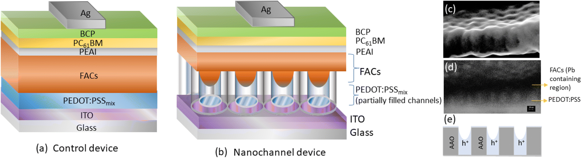 | ||
| Fig. 1 (a) Schematic structure of the control device and the (b) nanochannel HOIP device. The alumina nanochannels are partially filled with PEDOT:PSS and FACs (thickness of layers are not to scale). (c) Cross sectional SEM image of 20 nm AAO filled PEDOT:PSS and the FACs layers and (d) corresponding back scattered diffraction image revealing the filling of the lead containing (dark region) perovskite region through the length of alumina nanochannels. (e) shows a schematic of the hole transport path in nanochannel devices. | ||
Our previous reports50,51 have shown an increase in conductivity of PEDOT:PSS when confined in nanogeometries comparable to the transport length scales of the conducting polymer. The ordered domains and crystallinity of the nanoconfined polymers enhance the conductance of charge carriers along the nanochannel axes. This property of conducting polymer nanochannels is utilized to fabricate the nanochannel HOIP device. Usually the grade of PEDOT:PSS which contains a 1:6 ratio and has a work function of around 5.0 to 5.2 eV is generally used for photovoltaic applications. It has been earlier shown that the PH1000 grade of PEDOT:PSS which contains lower PSS content and work function around 4.8 to 5.0 eV is not suitable for a good amount of charge collection as it shows leakage current pathways. However, an optimized mixing of these two commercial grades can show improved behavior of the device performance. The two-probe IV characterization gives a high conductivity magnitude of 20 nm PEDOT:PSS mix' nanochannels with σtransverse ∼3.6 (±1.1) × 10−3 S cm−1. The surface morphology, wettability and transmittability of these two PEDOT:PSS types are shown in ESI S3.† The optimal growth and grain size of the perovskite films are dependent on the hydrophilicity of the underlying films which is the PEDOT:PSS HTL in the present case. Nonwetting surfaces have larger grains, thus smaller trap densities. Since the hydrophilicity of the PEDOT:PSS mix' is slightly less than that of pristine PEDOT:PSS, the FAC grains in contact with the HTL might be larger than in the former device which might be responsible for one of the factors for improved responsivity. However, the top surface of FACs doesn't show much change in grain size. The crystallinity of the two variations of PEDOT:PSS nanochannels using high resolution transmission electron microscopy is also shown in ESI S4.†
4.2. Electrical characterization and spectral analysis
Upon illuminating the HOIP device from the ITO side under open-circuit conditions, a photovoltage is developed across the interface VPV = Vlight − Vdark. The dark current essentially is the leakage current which originates from any trapped charge carriers or charge injection under reverse bias conditions. It is related to the crystal defects that result in the nonradiative recombination losses. The interface between the perovskite layer and the adjacent contact layers is important to analyze for reduced defects and match the energy levels. The electron transport layer PC61BM also plays an important role in passivating the charge defects and helps in reducing the current–voltage hysteresis due to trapped charges. Defects also get mitigated to some extent by adjusting the stoichiometric ratio of perovskite. Excess lead halide in the films has been shown to reduce nonradiative recombination significantly and thus improve the device performance.53 In this work, FA0.95Cs0.05Pb(I0.83Br0.17)3 stoichiometry has been found optimal for device performance. The HOIP photodetector device can be characterized by several figures of merit. A few of the parameters discussed below are photoresponsivity, external quantum efficiency, detectivity and response speed.The efficiency of the device's response to the light signals is given by a critical parameter called photoresponsivity. It is the ratio of the effective photocurrent generated by the photodetector due to the photon absorption and the incident light power, Pin and is given by:
 | (i) |
External quantum efficiency (EQE) indicates the sensitivity of the device. A part of the incident photons is absorbed to generate free electrons and holes. Again, due to recombination losses and trap defects, only a part of these photogenerated carriers can generate photocurrent. This limit of the device is quantified by EQE:
 | (ii) |
Specific detectivity which is another critical parameter can precisely reflect the limit of detecting light of lower intensities and is given by:
 | (iii) |
The I–V characteristics of the HOIP device obtained through the incidence of a continuous laser (532 nm) are depicted in Fig. 2a. A circular mask is used at the ITO side of the device to maintain the same area for all devices (Experimental setup shown in ESI S7†). The responsivity of bulk and nanochannel devices turns out to be 0.21 A W−1 and 0.29 A W−1, respectively, and the corresponding dark currents of the devices are Id(bulk) = 50 nA and Id(20 nm) = 21 nA. EQE values are 48.9% and 67.5%, respectively, for bulk and nanochannel devices. Specific detectivity is of the order 1.6 × 10¹² Jones and 3.5 × 10¹² Jones, respectively, for bulk and nanochannel devices from eqn (iii). For the voltage range −0.5 V < V < 1.0 V, higher magnitudes of responsivity are observed for nanochannel devices. The dark currents of 20 nm channel devices are lower than those of the bulk devices. Dark currents in terms of series resistances and effective contributing electrode area are elaborated in ESI S2.†
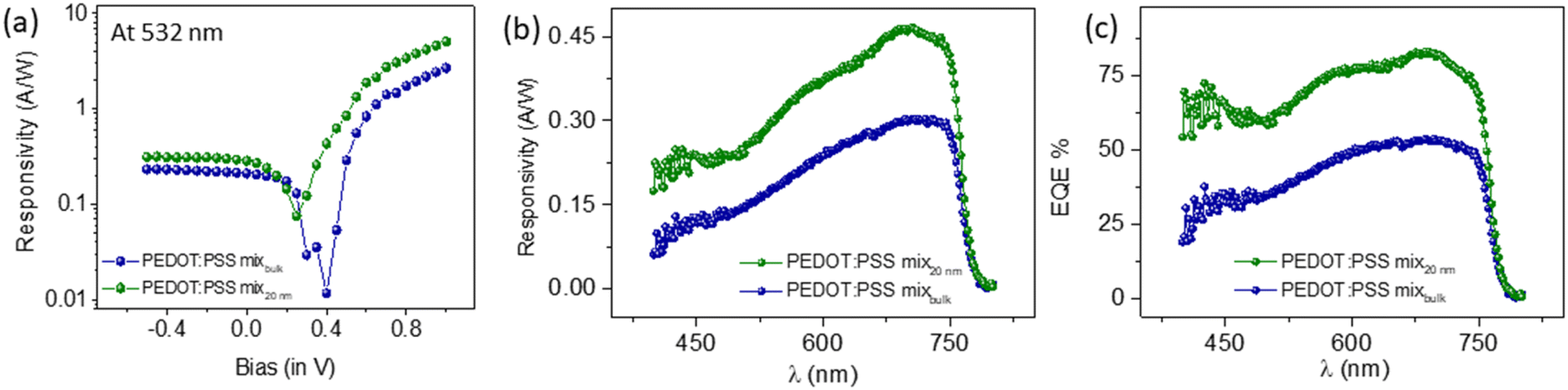 | ||
| Fig. 2 Electrical characterization. (a) Responsivity of the HOIP nanochannel and bulk device at 532 nm light source. (b) Responsivity and (c) EQE, respectively of the HOIP nanochannel and bulk devices over the spectral range. | ||
The responsivity and EQE measured over a wide spectrum of 400 nm < λ < 800 nm have been shown in Fig. 2b and c. Xenon lamp is used as a broadband light source which is coupled to a monochromator to produce a near monochromatic beam of light and a lock-in amplifier records the photocurrent signals from the HOIP device connected through a 50 Ω coupler. A mask with a 2 mm diameter hole is used before the devices on the ITO side to keep the incident illumination area the same for all devices. The photocurrent signal from a Si photodetector is used for calibration and all the measurements have been performed in a closed dark chamber. Using eqn (i)–(iii), at λ = 532 nm, PEDOT:PSS mix' bulk devices have transport numbers R = 0.18 A W−1, EQE = 41.9% and D = 1.4 × 10¹² Jones, while for the nanochannel devices, R = 0.28 A W−1, EQE = 65.2% and D = 3.4 × 10¹² Jones. Fig. 2b and c show higher magnitudes of responsivity and EQE at all wavelengths for nanochannel devices of the PEDOT:PSS mix' as compared to the bulk devices. The transport numbers are similar to those obtained while using laser light of 532 nm (Fig. 2a). The possible effect of moisture in nanochannel devices has been discussed in ESI S5.†
The response speed of the detectors is determined by the fall time, τ of the transient photocurrent to drop to 37% of its stable magnitude. Higher speed means shorter RC time constants and thus improved photodetector sensitivity. The response speed of the device is governed by the mobility of light-sensitive carriers and the effective distance between the two electrodes. Perovskites, being a direct bandgap material, have a high absorption coefficient and show high mobility of photogenerated carriers. Thus, enabling fast charge extraction leads to a fast response photodetector. Thus, a fast response photodetector is observed. In analyzing the small time taken for the carriers to travel the effective interelectrode distance, the smaller device area with lower capacitance showed the required RC time constant.54 A supercontinuum white light pulsed laser is used as a light source and triggered at the falling edge of the voltage pulse. The output signal is read from the oscilloscope. Fig. 3 shows shorter response time τ ∼ 40 ns for nanochannel HOIP while the bulk devices show τ ∼ 0.98 μs, which is nearly more than an order of magnitude higher than that of PEDOT nanochannel devices. The lower resistive PEDOT channels are mainly responsible for the faster time in nanochannel devices. The lower RC values for HOIP nanochannel devices give lower time scales and hence a faster response speed. Analyzing the transport parameters of the HOIP photodetector indicates that the nanochannel device performs more efficiently than their respective bulk devices.
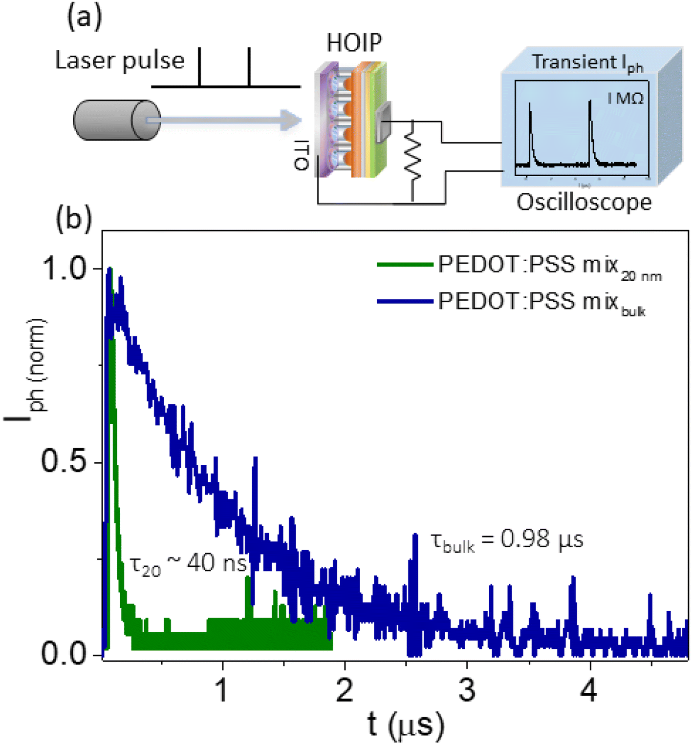 | ||
| Fig. 3 Transient photocurrent measurement. (a) Experimental setup using a pulsed supercontinuum laser source. (b) The response time, τ at the falling edge for HOIP bulk and nanochannel devices. | ||
5 Conclusion
A hybrid perovskite-based perovskite device incorporating a PEDOT:PSS-filled alumina scaffold has provided a platform to tune the electrical transport of charge carriers. The I(V) characteristics under dark and light conditions, EQE, detectivity and response timescales indicate improved performance parameters as compared to devices without the nanopores. This device architecture can open ways to achieve switching timescales in the sub-nanoseconds under reverse bias. The high conduction in confined PEDOT:PSS can be appropriately used in significantly improving performance in solar cells, batteries and light emitting diodes.Conflicts of interest
The authors declare no competing financial interest.Abbreviations
| PEDOT:PSS | poly(3,4-ethylenedioxythiophene):poly(styrenesulfonate) |
| CPs | Conducting polymers |
| ITO | Indium tin oxide |
| AAO | Anodized aluminum oxide |
| HRTEM | High resolution transmission electron microscopy |
Acknowledgements
S. D and N. G thank JNCASR facilities. The authors thank Sunoj K. R. for designing metal masks for physical vapor deposition. K. S. N acknowledges support from the DST-JC Bose fellowship.References
- M. M. Lee, et al., Efficient hybrid solar cells based on meso-superstructured organometal halide perovskites, Science, 2012, 338(6107), 643–647 CrossRef PubMed.
- Y.-C. Hsiao, et al., Fundamental physics behind high-efficiency organo-metal halide perovskite solar cells, J. Mater. Chem. A, 2015, 3(30), 15372–15385 RSC.
- S. A. Bretschneider, et al., Research update: physical and electrical characteristics of lead halide perovskites for solar cell applications, APL Mater., 2014, 2(4), 155204 Search PubMed.
- H.-S. Kim, et al., Mechanism of carrier accumulation in perovskite thin-absorber solar cells, Nat. Commun., 2013, 4(1), 2242 CrossRef PubMed.
- G. Xing, et al., Long-range balanced electron-and hole-transport lengths in organic-inorganic CH3NH3PbI3, Science, 2013, 342(6156), 344–347 CrossRef PubMed.
- T. C. Sum and N. Mathews, Advancements in perovskite solar cells: photophysics behind the photovoltaics, Energy Environ. Sci., 2014, 7(8), 2518–2534 RSC.
- M. Ahmadi, T. Wu and B. Hu, A review on organic–inorganic halide perovskite photodetectors: device engineering and fundamental physics, Adv. Mater., 2017, 29(41), 1605242 CrossRef PubMed.
- N. Chen, et al., Universal Band Alignment Rule for Perovskite/Organic Heterojunction Interfaces, ACS Energy Lett., 2023, 8(3), 1313–1321 CrossRef.
- M. I. Saleem, et al., Suppression of mid-gap trap state in CsPbBr3 Nanocrystals with Br-passivation for Self-Powered Photodetector, Energy Technol., 2023, 11(7), 2300013 CrossRef.
- M. Sulaman, et al., Lead-free tin-based perovskites nanocrystals for high-performance self-driven bulk-heterojunction photodetectors, Mater. Today Phys., 2022, 27, 100829 CrossRef.
- M. Sulaman, et al., Two Bulk-Heterojunctions Made of Blended Hybrid Nanocomposites for High-Performance Broadband, Self-Driven Photodetectors, ACS Appl. Mater. Interfaces, 2023, 15(21), 25671–25683 CrossRef PubMed.
- M. Qasim, et al., High-performance Self-powered Broadband Schottky Junction Photodetector based on Graphene–Silicon van der Waals Heterostructure, Energy Technol., 2023, 11(10), 2300492 CrossRef.
- M. Razeghi and A. Rogalski, Semiconductor ultraviolet detectors, J. Appl. Phys., 1996, 79(10), 7433–7473 CrossRef.
- G. Konstantatos, et al., Ultrasensitive solution-cast quantum dot photodetectors, Nature, 2006, 442(7099), 180–183 CrossRef PubMed.
- A. Motmaen, A. Rostami and S. Matloub, Ultra high-efficiency integrated mid infrared to visible up-conversion system, Sci. Rep., 2020, 10(1), 1–10 CrossRef PubMed.
- L. Shi, et al., Status and outlook of metal–inorganic semiconductor–metal photodetectors, Laser Photonics Rev., 2021, 15(1), 2000401 CrossRef.
- Q. Chen, et al., Schottky barrier detectors on GaN for visible–blind ultraviolet detection, Appl. Phys. Lett., 1997, 70(17), 2277–2279 CrossRef.
- F. Koppens, et al., Photodetectors based on graphene, other two-dimensional materials and hybrid systems, Nat. Nanotechnol., 2014, 9(10), 780–793 CrossRef PubMed.
- S. Shafique, et al., High-performance photodetector using urchin-like hollow spheres of vanadium pentoxide network device, Sens. Actuators, A, 2019, 296, 38–44 CrossRef.
- M. Usman, et al., Polarization-Sensitive Photodetection of Anisotropic 2D Black Arsenic, J. Phys. Chem. C, 2023, 127(19), 9076–9082 CrossRef.
- A. Imran, et al., Electric-Dipole Gated Two Terminal Phototransistor for Charge-Coupled Device, Adv. Opt. Mater., 2023, 2300910 CrossRef.
- H. Chen, et al., Flexible optoelectronic devices based on metal halide perovskites, Nano Res., 2020, 13, 1997–2018 CrossRef.
- F. P. García de Arquer, et al., Solution-processed semiconductors for next-generation photodetectors, Nat. Rev. Mater., 2017, 2(3), 1–17 Search PubMed.
- Z.-K. Tan, et al., Bright light-emitting diodes based on organometal halide perovskite, Nat. Nanotechnol., 2014, 9(9), 687–692 CrossRef PubMed.
- H. C. Kwon, et al., Parallelized nanopillar perovskites for semitransparent solar cells using an anodized aluminum oxide scaffold, Adv. Energy Mater., 2016, 6(20), 1601055 CrossRef.
- X. Yin, et al., Toward ideal hole transport materials: a review on recent progress in dopant-free hole transport materials for fabricating efficient and stable perovskite solar cells, Energy Environ. Sci., 2020, 13(11), 4057–4086 RSC.
- H. D. Pham, et al., Organic interfacial materials for perovskite-based optoelectronic devices, Energy Environ. Sci., 2019, 12(4), 1177–1209 RSC.
- S. Demchyshyn, et al., Confining metal-halide perovskites in nanoporous thin films, Sci. Adv., 2017, 3(8), e1700738 CrossRef PubMed.
- S. Guarnera, et al., Improving the long-term stability of perovskite solar cells with a porous Al2O3 buffer layer, J. Phys. Chem. Lett., 2015, 6(3), 432–437 CrossRef PubMed.
- Y. Wang, et al., PTAA as Efficient Hole Transport Materials in Perovskite Solar Cells: A Review, Sol. RRL, 2022, 6(8), 2200234 CrossRef.
- W. Chen, et al., Alkali chlorides for the suppression of the interfacial recombination in inverted planar perovskite solar cells, Adv. Energy Mater., 2019, 9(19), 1803872 CrossRef.
- F. Jiang, et al., Post-treatment-free solution-processed non-stoichiometric NiOx nanoparticles for efficient hole-transport layers of organic optoelectronic devices, Adv. Mater., 2015, 27(18), 2930–2937 CrossRef PubMed.
- Q. Niu, et al., Understanding the mechanism of PEDOT: PSS modification via solvent on the morphology of perovskite films for efficient solar cells, Synth. Met., 2018, 243, 17–24 CrossRef.
- J. Y. Jeng, et al., CH3NH3PbI3 perovskite/fullerene planar-heterojunction hybrid solar cells, Adv. Mater., 2013, 25(27), 3727–3732 CrossRef PubMed.
- S.-I. Na, et al., Evolution of nanomorphology and anisotropic conductivity in solvent-modified PEDOT:PSS films for polymeric anodes of polymer solar cells, J. Mater. Chem., 2009, 19(47), 9045–9053 RSC.
- W. Zhang, et al., High-efficiency ITO-free polymer solar cells using highly conductive PEDOT: PSS/surfactant bilayer transparent anodes, Energy Environ. Sci., 2013, 6(6), 1956–1964 RSC.
- Z. Zhao, et al., Improving the conductivity of PEDOT: PSS hole transport layer in polymer solar cells via copper (II) bromide salt doping, ACS Appl. Mater. Interfaces, 2015, 7(3), 1439–1448 CrossRef PubMed.
- L. Mazzarella, et al., Infrared light management using a nanocrystalline silicon oxide interlayer in monolithic perovskite/silicon heterojunction tandem solar cells with efficiency above 25%, Adv. Energy Mater., 2019, 9(14), 1803241 CrossRef.
- C. Yi, et al., Entropic stabilization of mixed A-cation ABX 3 metal halide perovskites for high performance perovskite solar cells, Energy Environ. Sci., 2016, 9(2), 656–662 RSC.
- D. P. McMeekin, et al., A mixed-cation lead mixed-halide perovskite absorber for tandem solar cells, Science, 2016, 351(6269), 151–155 CrossRef PubMed.
- M. Saliba, et al., Cesium-containing triple cation perovskite solar cells: improved stability, reproducibility and high efficiency, Energy Environ. Sci., 2016, 9(6), 1989–1997 RSC.
- E. Planes, et al., Degradation mechanisms in a mixed cations and anions perovskite solar cell: mitigation effect of the gold electrode, ACS Appl. Energy Mater., 2021, 4(2), 1365–1376 CrossRef.
- K. Jäger, et al., Numerical optical optimization of monolithic planar perovskite-silicon tandem solar cells with regular and inverted device architectures, Opt. Express, 2017, 25(12), A473–A482 CrossRef PubMed.
- N. Ganesh, et al., 2D position-sensitive hybrid-perovskite detectors, ACS Appl. Mater. Interfaces, 2021, 13(45), 54527–54535 CrossRef PubMed.
- A. Mandal, et al., Photodetectors with high responsivity by thickness tunable mixed halide perovskite nanosheets, ACS Appl. Mater. Interfaces, 2021, 13(36), 43104–43114 CrossRef PubMed.
- T. Yang, F. Li and R. Zheng, Recent progress on cesium lead halide perovskites for photodetection applications, ACS Appl. Electron. Mater., 2019, 1(8), 1348–1366 CrossRef.
- L. Lv, et al., Generalized colloidal synthesis of high-quality, two-dimensional cesium lead halide perovskite nanosheets and their applications in photodetectors, Nanoscale, 2016, 8(28), 13589–13596 RSC.
- D. J. Kubicki, et al., Phase segregation in Cs-, Rb-and K-doped mixed-cation (MA)x (FA)1−x PbI3 hybrid perovskites from solid-state NMR, J. Am. Chem. Soc., 2017, 139(40), 14173–14180 CrossRef PubMed.
- Y. Yu, et al., Improving the performance of formamidinium and cesium lead triiodide perovskite solar cells using lead thiocyanate additives, ChemSusChem, 2016, 9(23), 3288–3297 CrossRef PubMed.
- S. Das, A. Kumar and K. Narayan, Confinement highlights the different electrical transport mechanisms prevailing in conducting polymers, Phys. Rev. Mater., 2022, 6(2), 025602 CrossRef.
- S. Das and K. S. Narayan, Significant Increase in Electrical Transport of Conducting Polymers Confined in Alumina Nanopores, J. Phys. Chem. C, 2019, 123(17), 11284–11291 CrossRef.
- S. Das, et al., Ordered and disordered microstructures of nanoconfined conducting polymers, Soft Matter, 2023, 19(29), 5641–5650 RSC.
- Q. Chen, et al., Controllable self-induced passivation of hybrid lead iodide perovskites toward high performance solar cells, Nano Lett., 2014, 14(7), 4158–4163 CrossRef PubMed.
- L. Shen, et al., A self-powered, sub-nanosecond-response solution-processed hybrid perovskite photodetector for time-resolved photoluminescence-lifetime detection, Adv. Mater., 2016, 28(48), 10794–10800 CrossRef PubMed.
Footnote |
| † Electronic supplementary information (ESI) available: Device architecture and the SEM image of 20 nm AAO; the calculation of the effective surface area of the nanochannel device under dark and light conditions; the surface morphology, optical transmission and contact angle measurements of PEDOT:PSS mix' and PEDOT:PSS; the crystallinity of the two types of PEDOT:PSS in nanochannels using high resolution transmission electron microscopy; moisture effect on the nanochannel devices; FACs surface roughness; experimental setup used for measuring the photocurrent and voltage characteristics. See DOI: https://doi.org/10.1039/d3na00485f |
| This journal is © The Royal Society of Chemistry 2023 |