
 Open Access Article
 This Open Access Article is licensed under a Creative Commons Attribution-Non Commercial 3.0 Unported Licence
New insights into the influence of plasmonic and non-plasmonic nanostructures on the photocatalytic activity of titanium dioxide†
Anna
Jakimińska
 ab,
Kaja
Spilarewicz
a and
Wojciech
Macyk
*a
ab,
Kaja
Spilarewicz
a and
Wojciech
Macyk
*a
aFaculty of Chemistry, Jagiellonian University, Ul. Gronostajowa 2, 30-387 Kraków, Poland. E-mail: macyk@chemia.uj.edu.pl
bDoctoral School of Exact and Natural Sciences, Jagiellonian University, Ul. S. Łojasiewicza 11, 30-348 Kraków, Poland
First published on 4th October 2023
Abstract
The results of this work cover the influence of plasmonic (gold) and non-plasmonic (palladium) nanostructures on the photocatalytic activity and redox properties of titanium dioxide. Materials decorated with gold, palladium and both materials were examined using photoelectrochemical and spectroelectrochemical methods to establish the changes introduced by the modifications and the possibility of the influence of the plasmonic effect from gold on their activity. Additionally, the photocatalytic tests of hydroxyl radical generation and hydrogen evolution were performed to confirm the activity of modified materials in oxidation and reduction reactions. It turned out that in the observed system the catalytic properties of palladium determine mostly the activity of modified materials, and the surface plasmon resonance of gold does not affect the activity. Moreover, the influence of the nanostructures on the activity, besides the catalytic performance, is the same for plasmonic and non-plasmonic ones and results in a change in the redox properties of the semiconductor.
Introduction
Modification of titanium dioxide with metallic nanostructures is one of the most explored topics in terms of activity enhancement of this material. There are many reports on the mechanisms of the activity increment of semiconductors in the presence of metallic nanostructures,1–5 however, they are still inconsistent. Considering the modification with plasmonic nanostructures, the mechanisms often involve hot electron transfer, local field enhancement or energy transfer from the plasmonic nanostructure to the semiconductor. However, the hypothesized mechanisms in some cases are questionable.6,7 Most of the authors agree that the plasmonic properties depend on the nanostructures' size, composition and environment.8,9 For instance, the sizes for which they observe hot electron injection are different in various cases, although the substrate is the same.2,10,11 Or, the local field enhancement is thought to be responsible for the increase in the activity in the surface plasmon resonance (SPR) absorption range of the semiconductor that cannot absorb light that induces SPR.12 There are also some thorough reports providing evidence of the possibility of plasmonic effect utilization.13–15 The non-plasmonic nanostructures are, in contrast, used as electron sinks16 or catalytic sites.17 Despite the name, the non-plasmonic nanostructures exhibit surface plasmon resonance. However, the SPR band, in this case, covers an inconvenient range of light (in terms of photocatalysis). Therefore, they are considered non-plasmonic components of the system.18 To tune the properties of both types of nanostructures and combine their advantageous properties, the use of bi-metallic modifications is employed. Often the alloyed or core–shell nanostructures are synthesized19,20 but the modification with two metals separated at the substrate surface is also known.21 One of the interesting approaches is the use of plasmonic nanostructures as antennas for the non-plasmonic ones.22 In this case, there is no enhancement in the semiconductor activity caused by the plasmonic effect. Instead, this effect is used to enhance the catalytic properties of the non-plasmonic active centers. Therefore, the exact phenomena occurring in the photocatalytic systems can strongly depend on the kind of metal and should be carefully recognized.In this work, two metals, gold and palladium were selected to examine the behaviour of plasmonic and non-plasmonic nanostructures, respectively, deposited on titanium dioxide. The influence of catalytic properties and the impact of the size of nanostructures on photoactivity and redox properties of the semiconductor were explored. Moreover, for a better overview, samples modified with both metals simultaneously were examined.
Results and discussion
Gold and palladium were selected to examine the influence of the plasmonic and non-plasmonic metallic nanostructures on the photocatalytic properties of titanium dioxide. TiO2 was modified by the photodeposition of the metals on the surface. The photodeposition was carried out for 60 s or 10 min and the obtained samples were denoted as A60sPd and A10minPd for modification with palladium, A60sAu and A10minAu for modification with gold, and A60sAuPd and A10minAuPd for modification with both metals (A stands for the TiO2 anatase phase). More experimental details are provided in the ESI.† The time of photodeposition was selected to obtain a significant difference in the size and amounts of the nanostructures. A longer time enables the formation of more stable nanostructures as the equilibrium in the growth process can be achieved, while at the beginning it can be disturbed inter alia by Ostwald ripening.23 The presence of metallic nanostructures in the modified materials was established by scanning electron microscopy and EDS spectroscopy. Fig. 1 and S1† reveal the successful deposition of palladium, gold and both metals simultaneously after photodeposition. It is well-known that gold can be deposited more easily, thus it is not surprising that in the case of this metal, the number of nanostructures is the highest.24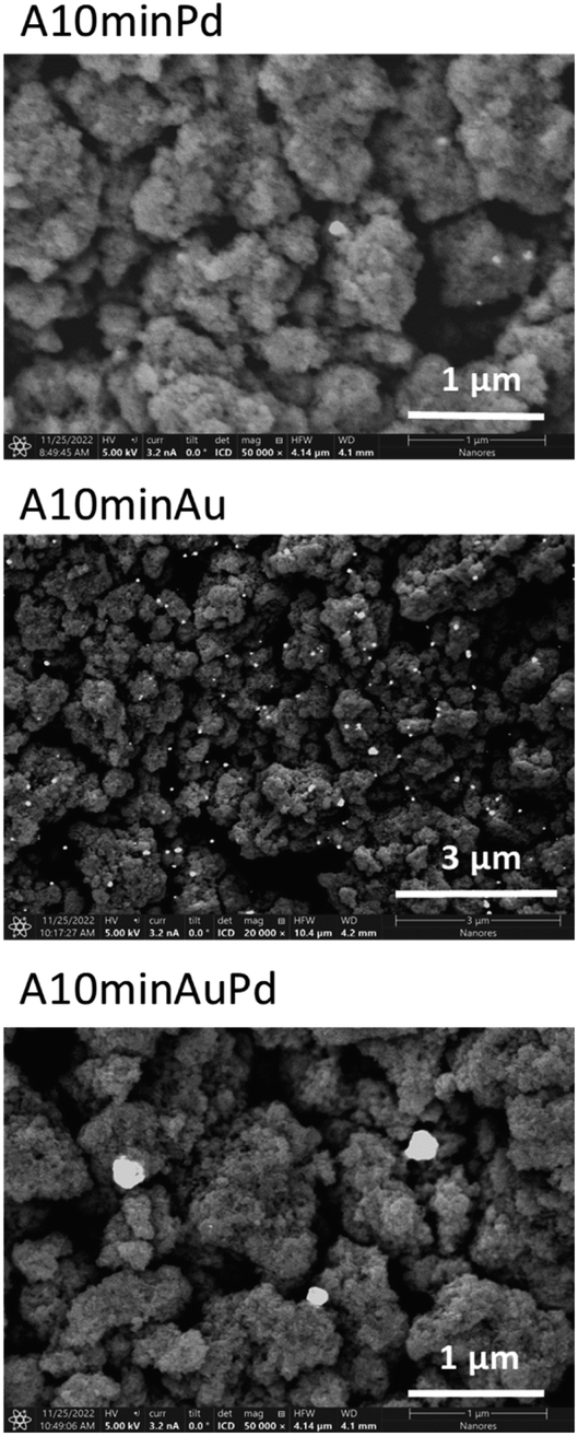 | ||
| Fig. 1 SEM images of decorated materials (after 10 min of photodeposition). | ||
The spectral properties of the studied composites were analysed using DRS (Fig. 2 and S2†). As can be noticed, the presence of the nanostructures has no significant effect on the absorption edge position, and, therefore, on the bandgap value. The maximal hypsochromic shift can be observed for materials modified with palladium resulting in a bandgap increment. Nevertheless, the change is not very pronounced (from 3.21 eV for bare anatase to 3.28 eV for A10minPd). The SPR band is clearly visible only for materials modified with gold, in the range characteristic of this metal, i.e. 500 to 600 nm.25 This band is more intense for A10minAu than for A60sAu which is typical for larger particles. By diminishing the size of gold nanoparticles, absorption intensity, as well as the relative contribution of scattering to the absorption, rapidly decreases.26 The SPR band is wide due to the polydispersity of the nanoparticles, which originates from the growth kinetics. Palladium at the same time is considered a non-plasmonic noble metal (along with platinum, rhodium, etc.),27 therefore, there is no visible SPR band for the materials modified with this metal. However, there are some reports on a weak SPR band of Pd nanoparticles present below 400 nm, therefore, overlapping with the absorption band of titanium dioxide and its Urbach tail.28,29 Nevertheless, in the presented spectra no evidence of such a band can be observed (Fig. S2†). In the case of materials modified with both metal structures, the SPR band is present only for A10minAuPd, and it is visible in the same range as for the gold-modified materials, indicating the prevalent influence of gold SPR (Fig. S2†). The lower intensity of this band can be either the effect of a lower amount of gold nanoparticles or the damping caused by the presence of palladium.30 The phenomenon of SPR damping is a result of the influence of Pd interband transitions which occur at lower frequency in comparison to Au.8 Similar observations were also described by Kanungo et al.31 and Zhan et al.32
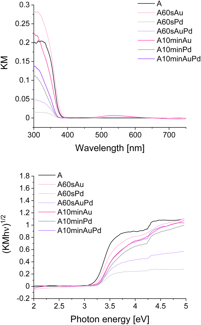 | ||
| Fig. 2 DRS spectra in KM representation (upper picture) and Tauc plots for bare and modified materials (lower picture). | ||
To reveal the influence of the nanoparticles on the photoactivity of the synthesized systems and get some insights into their redox properties, photocurrent measurements were performed (Fig. 3). Small nanostructures shift the Fermi level (EF) towards higher potentials compared to the bare material (anodic shift of the switch point) and cathodic photocurrents appear. This may indicate the behaviour of the structures as electron sinks suppressing charge carrier recombination. Moreover, as evidenced by cathodic currents, metal nanostructures collecting electrons can improve the reductive properties of modified materials. The process of electron transfer from the excited semiconductor to the metal ions adsorbed at the surface and later metal clusters is the driving force for the nanoparticle growth through the photodeposition method. However, after a prolonged time of photodeposition, when the larger nanostructures emerge, the Fermi level shifts towards lower potentials as evidenced by the disappearance of cathodic photocurrents and the absence of a photocurrent switch on the IPCE maps. The photocurrent measurements are insufficient to fully explain the exact reason for this phenomenon. From the obtained data, it can be assumed that the processes of the electron transfer to the environment have to be suppressed, and may result in the worse catalytic properties of larger nanostructures, in accordance with photocatalytic tests (vide infra). Nevertheless, the charge separation in such systems still can be significantly higher than for the bare material.
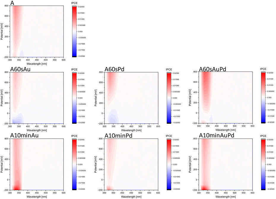 | ||
| Fig. 3 IPCE maps (vs. potential and wavelength) of bare and modified materials. | ||
The phenomenon of observed Fermi level shifts may be related to the change in the Fermi level of nanostructures during their growth and its simultaneous equilibration in the system. It was evidenced that with the change in the nanostructure size, the Fermi level differs significantly.33–35 Usually with the increase in the nanoparticle diameter, the Fermi level energy decreases.33,35,36 Such an effect is in contrast to the behaviour observed during our measurements. However, there are also reports in accordance with our findings.37–39 These apparent discrepancies can be justified, as it is worth noting that the nanoparticles were synthesized with different procedures and sometimes organic linkers were used to attach the nanoparticles to the electrode substrate. Moreover, various substrates with different Fermi levels were used throughout these studies. Described differences cannot be ignored. Scanlon et al. mentioned the importance of the nanoparticle charging in terms of their EF positions, e.g., due to the adsorption of the stabilizers or the redox-active species from the environment.34 Moreover, Kiyonaga et al. ascribed the difference in the trend of the Fermi level change with the increase of the nanoparticle diameter due to the hydration of the nanostructures,37 and Das et al. state that the EF increases with the increase in nanoparticle loading and not with the change in their size.39 Our studied system was examined in water, and the loading with nanostructures deposited at longer irradiation times was higher. Thus, all the discussed effects can contribute to the observed shifts in EF.
Noteworthily, there is no significant difference between plasmonic and non-plasmonic structures evidenced by photocurrent measurements (Fig. 3 and S3†). The maps are intensity corrected, thus the absence of higher photocurrent in the range of the SPR band of gold points to the lack of activity in this region. This indicates no plasmonic enhancement of the photoactivity of the system. Therefore, the observations lead to the conclusion that the effect of size and loading of metal onto the semiconductor prevail over the assumed plasmonic effects.
To further investigate the redox properties of the decorated materials, spectroelectrochemical measurements were performed to establish their conduction band (CB) edge potentials.40 To determine the influence of the nanoparticles, the reference and modified materials were examined. It was found that the electronic states under the conduction band edge, creating the Urbach tail and surface defects of the semiconductor, are no longer available after nanostructure deposition, and their density decreases with the increase of the particle size and loading resulting in the conduction band edge shift towards lower potentials (Fig. 4).
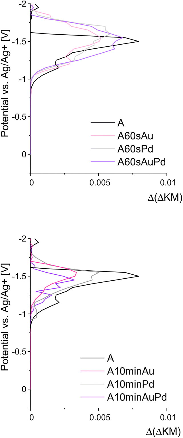 | ||
| Fig. 4 Results of spectroelectrochemical measurements depicting the density of electronic states in the vicinity of conduction band edges of the materials. | ||
These results along with DRS allow for further recognition of the redox properties of the materials. According to the DRS measurements, upon modifications, the absorption edge shifted only slightly (Fig. 2) and therefore, the bandgap changed negligibly (by about 0.07 eV). At the same time, the conduction band edge shifted by approximately 0.1 V for smaller nanostructures and around 0.2 V for larger ones (Fig. 4). Therefore, there is a possibility of a change in the redox properties of the materials after nanostructures' deposition. As for smaller nanostructures, the shift is less pronounced, while the bandgap increase remains the same (in comparison to larger nanostructures), it can be concluded that the growth of nanostructures results in the disappearance of some electronic states and therefore the bandgap widening. Therefore, the redox properties are affected insignificantly, but the impact of enhanced charge carrier separation on the photoactivity cannot be neglected. For larger structures, the CB band edge is shifted by ca. 0.2 V. Therefore, the shift of the valence band by around 0.1 V towards lower potentials should occur. Such an effect can influence the oxidative properties of the materials, i.e., they can be slightly worse oxidizers than before the modification. The difference of 0.1 V is not very significant, however, it can be at least one of the reasons for the shift of the Fermi level towards lower potentials observed on the IPCE maps for the materials modified with larger nanostructures. A schematic representation of the described changes is provided in Fig. 5.
 | ||
| Fig. 5 The scheme of the changes introduced to the states' distribution and band edge potentials after the growth of metallic nanostructures (depicted as violet dots). | ||
The spectroelectrochemical measurements also revealed no differences between the behaviour of plasmonic and non-plasmonic nanostructures. Both types cause the decrease in the availability of the states under the CB edge, which served as the nucleation centers for their growth, and influence the redox properties of the semiconductor in the same way.
To examine the properties of the materials in photocatalytic reduction and oxidation processes, a few types of tests were performed. To evaluate the nanostructures' influence on oxidation and reduction, the tests of terephthalic acid oxidation and water splitting, respectively, were selected. Observation of hydroxyterephthalic acid appearance in the system indicates the formation of hydroxyl radicals during photocatalytic oxidation of water. Similarly, the determination of hydrogen from the water splitting points to the reductive properties of the materials as the hydrogen is the product of water reduction during water splitting. By examining these two processes separately, one can notice possible differences in the redox properties of the materials outlined in previous measurements. The results of mentioned photocatalytic tests, performed under simulated solar light, are presented in Fig. 6.
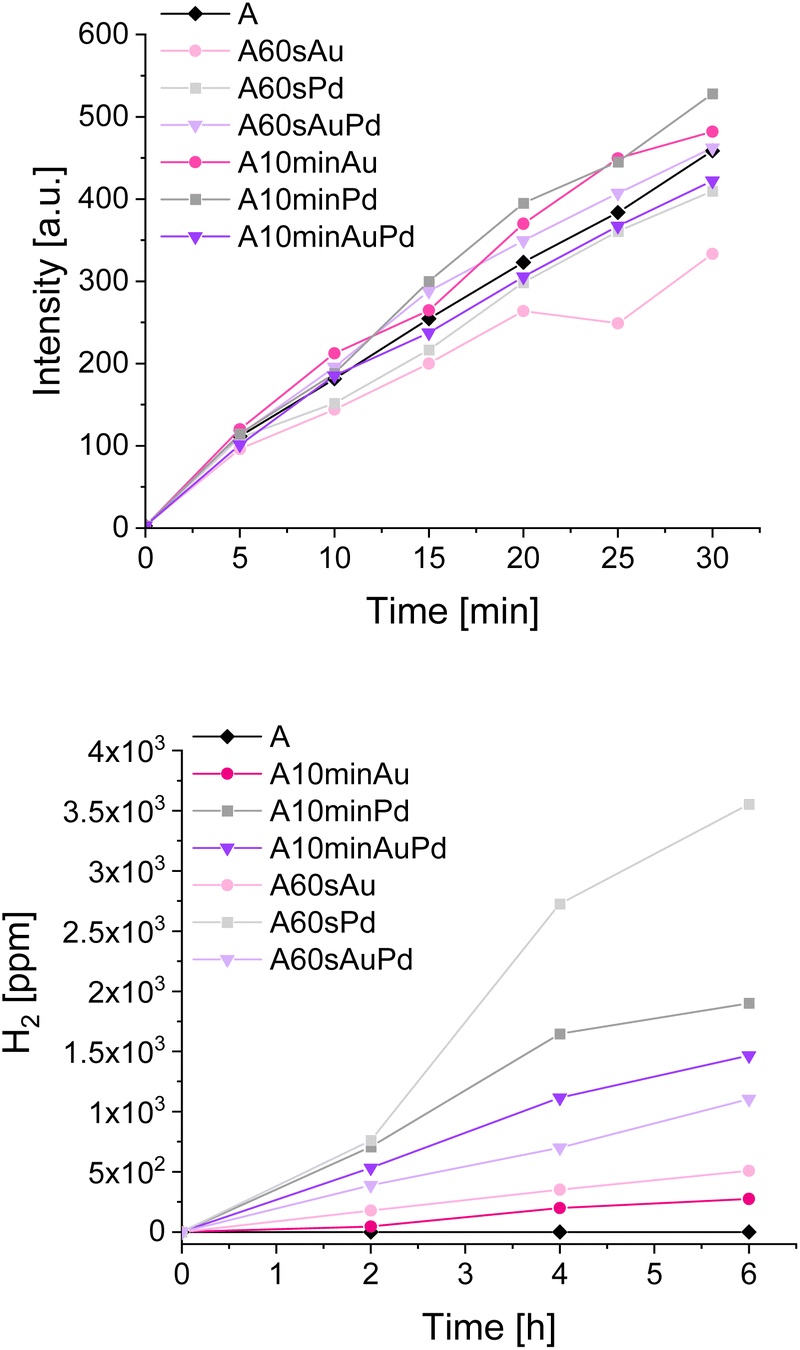 | ||
| Fig. 6 Tests with terephthalic acid oxidation (upper picture) and water splitting (lower picture). | ||
The tests of water oxidation to form hydroxyl radicals show no significant differences between bare and modified materials. This is in line with the observations made during photoelectrochemical and spectroelectrochemical tests as the oxidative properties of the materials should not differ significantly. The negligible increase in the activity for some materials may be ascribed to the better charge separation in modified materials which seems to be more pronounced for materials with larger nanostructures. The influence of deposited metals on oxidative properties can be thus considered almost insignificant. In contrast, a significant impact can be observed during water splitting tests. The amount of evolved hydrogen is higher for the materials decorated with smaller nanostructures compared to their counterparts with larger ones. It can be clearly seen that the materials after 60 s of photodeposition exhibit better reductive properties which corroborate with the photoelectrochemical measurements and also is indicated by the CB shift evidenced during spectroelectrochemical measurements.
The difference between gold and palladium nanostructures, which should be expected due to their plasmonic and non-plasmonic behaviour, emerges exclusively in the hydrogen evolution. The outstanding performance of palladium-modified titanium dioxide (compared to other samples) is the result of the catalytic properties of this metal encompassing the great hydrogen absorption and its unusual bonding in atomic form which is very advantageous for pure hydrogen formation.41 However, despite the nature of metal, the samples with smaller nanostructures are more active than those with larger ones. This trend is reversed only for the samples modified with both metals simultaneously and can be ascribed to the higher content of palladium in the sample after 10 minutes of photodeposition which results in a higher hydrogen evolution rate. Thus, it is evidenced that the catalytic properties of this metal prevail over the influence of nanostructures on the material's redox properties.
The photocatalytic tests of hydroxyterephthalic acid formation were performed also under visible light (λ > 420 nm), which revealed that the modified TiO2 exhibits lower activity in comparison to the bare material in oxidation processes (Fig. S4†). This phenomenon can be ascribed to the widening of the bandgap and the unavailability of the states that were responsible for the absorption in this range for the bare material. Additionally, the water splitting tests were also conducted, however, the amounts of produced hydrogen were near the noise level, which, taking into account the accuracy of the method, disabled to designate the trends and comparison of the samples. Therefore, the presence of gold seems not to be advantageous in terms of visible light activity.
To additionally confirm the redox properties of the system, the methanol dehydrogenation was performed under simulated solar light, and the amount of hydrogen evolved in this reaction was monitored (Fig. 7). The process consists of both oxidation and reduction parts,42 therefore, it was selected as the link that connects the previously examined reductive and oxidative paths and also involves the catalytic properties of palladium. It turned out that in this case, the catalytic effect prevails as well. However, in terms of this process, the amount of palladium seems to be of stronger importance than the redox properties and nanoparticle size. Therefore, the catalytic effect boosts the photocatalytic activity and is strictly dependent on the amount of palladium. In terms of TiO2 modified with gold, the trend remains the same as for water splitting, as in this case only redox properties are involved. On the basis of these outcomes, it can be noticed that the non-plasmonic nanoparticles can be even more beneficial for some photocatalytic processes than widely investigated plasmonic nanostructures.
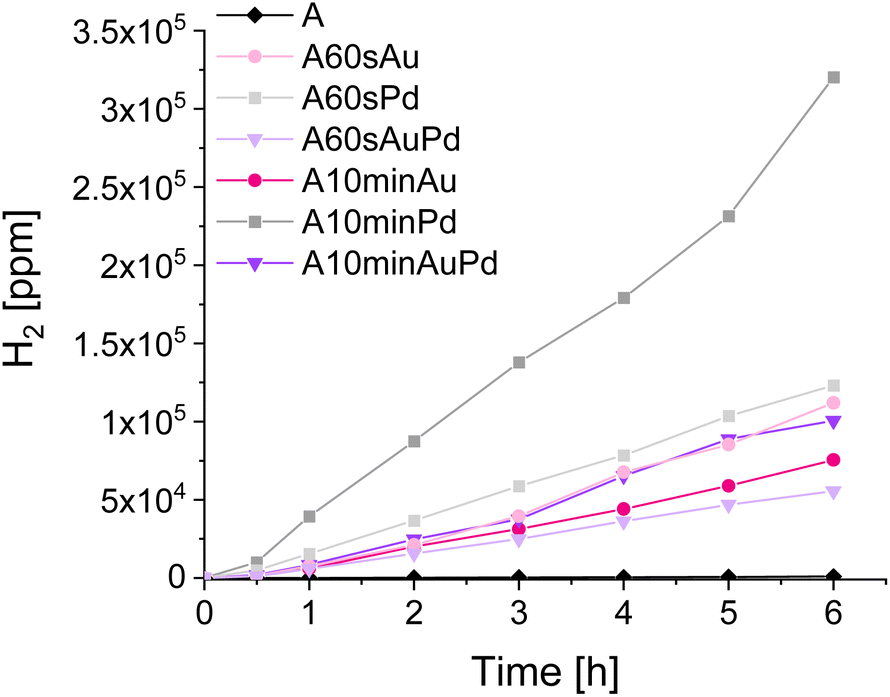 | ||
| Fig. 7 Methanol dehydrogenation tests under simulated solar light. | ||
Conclusions
In this work, the effect of plasmonic and non-plasmonic nanostructures deposited on titanium dioxide on the redox properties of this material was examined. It was found that the size and amounts of nanostructures or their catalytic properties have a greater influence on the photocatalytic activity of TiO2 than their interaction with light since no influence of plasmonic properties of gold was recognized in the examined system, despite the observed SPR signal. This shows, that conclusions on the role of plasmonic nanoparticles as photosensitizers must be very well evidenced, for instance with intensity-corrected photoaction spectra. It was established that the surface states of the TiO2 act as the centers of nucleation for metallic nanoparticles, therefore, they are occupied during the nanoparticle growth. When this process is extensive, it results in the shift of the conduction band edge and the change in the redox properties of the materials. This phenomenon can be thus considered the main factor influencing the photoactivity of metallic nanoparticle-modified titanium dioxide.Author contributions
Conceptualization: A. J. and K. S.; data curation: A. J.; formal analysis: A. J. and W. M.; funding acquisition: W. M.; investigation: A. J. and K. S.; methodology: A. J. and K. S.; supervision: W. M.; validation: A. J. and K. S.; visualization: A. J.; writing – original draft: A. J.; writing – review & editing: A. J., K. S. and W. M.Conflicts of interest
There are no conflicts to declare.Acknowledgements
The authors would like to acknowledge the National Science Centre in Poland for financial support under the grant Solar-Driven Chemistry (2019/01/Y/ST5/00027). Moreover, we are grateful to Nanores (Wrocław, Poland) for the SEM images and EDS analysis.References
- M. A. Ibrahem, B. G. Rasheed, R. I. Mahdi, T. M. Khazal, M. M. Omar and M. O'Neill, RSC Adv., 2020, 10, 22324, 10.1039/D0RA03858J.
- S. K. Cushing, J. Li, J. Bright, B. T. Yost, P. Zheng, A. D. Bristow and N. Wu, J. Phys. Chem. C, 2015, 119, 16239–16244, DOI:10.1021/acs.jpcc.5b03955.
- X.-C. Ma, Y. Dai, L. Yu and B.-B. Huang, Light: Sci. Appl., 2016, 5, e16017, DOI:10.1038/lsa.2016.17.
- T. Bora, D. Zoepfl and J. Dutta, Sci. Rep., 2016, 6, 26913, DOI:10.1038/srep26913.
- P. Li, Y. Ouyang, G. Xiao, Y. Zhao, S. Sarina, J. Baeyens, H. Su and H.-Y. Zhu, Green Chem., 2021, 23, 7780–7789, 10.1039/D1GC01953H.
- S. Mihai, D. L. Cursaru, D. Ghita and A. Dinescu, Mater. Lett., 2016, 162, 222–225, DOI:10.1016/j.matlet.2015.10.012.
- K. K. Paul, P. K. Giri, H. Sugimoto, M. Fujii and B. Choudhury, Sol. Energy Mater. Sol. Cells, 2019, 201, 110053, DOI:10.1016/j.solmat.2019.110053.
- V. Amendola, R. Pilot, M. Frasconi, O. M. Maragò and M. A. Iatì, J. Phys.: Condens. Matter, 2017, 29, 203002, DOI:10.1088/1361-648X/aa60f3.
- M. M. Abouelela, G. Kawamura and A. Matsuda, J. Clean. Prod., 2021, 294, 126200, DOI:10.1016/j.jclepro.2021.126200.
- Y. Shiraishi, N. Yasumoto, J. Imai, H. Sakamoto, S. Tanaka, S. Ichikawa, B. Ohtani and T. Hirai, Nanoscale, 2017, 9, 8349–8361, 10.1039/C7NR02310C.
- G. Žerjav, M. Roškarič, J. Zavašnik, J. Kovač and A. Pintar, Appl. Surf. Sci., 2022, 579, 152196, DOI:10.1016/j.apsusc.2021.152196.
- Z. Liu, W. Hou, P. Pavaskar, M. Aykol and S. B. Cronin, Nano Lett., 2011, 11, 1111–1116, DOI:10.1021/nl104005n.
- B. Foerster, M. Hartelt, S. S. E. Collins, M. Aeschlimann, S. Link and C. Sönnichsen, Nano Lett., 2020, 20, 3338–3343, DOI:10.1021/acs.nanolett.0c00223.
- M. J. Kale, T. Avanesian and P. Christopher, ACS Catal., 2014, 4, 116–128, DOI:10.1021/cs400993w.
- C. Boerigter, R. Campana, M. Morabito and S. Linic, Nat. Commun., 2016, 7, 10545, DOI:10.1038/ncomms10545.
- X. Guo, L. Kong, J. Xu, J. Chen and L. Li, Dalton Trans., 2021, 50, 9529–9539, 10.1039/D1DT00910A.
- S. Bai, X. Wang, C. Hu, M. Xie, J. Jiang and Y. Xiong, Chem. Commun., 2014, 50, 6094–6097, 10.1039/C4CC00745J.
- Z. H. N. Al-Azri, W.-T. Chen, A. Chan, V. Jovic, T. Ina, H. Idriss and G. I. N. Waterhouse, J. Catal., 2015, 329, 355–367, DOI:10.1016/j.jcat.2015.06.005.
- A. Zaleska-Medynska, M. Marchelek, M. Diak and E. Grabowska, Adv. Colloid Interface Sci., 2016, 229, 80–107, DOI:10.1016/j.cis.2015.12.008.
- K. Sytwu, M. Vadai and J. A. Dionne, Adv. Phys.: X, 2019, 4, 1619480, DOI:10.1080/23746149.2019.1619480.
- M. Vadai, D. K. Angell, F. Hayee, K. Sytwu and J. A. Dionne, Nat. Commun., 2018, 9, 4658, DOI:10.1038/s41467-018-07108-x.
- K. Li, N. J. Hogan, M. J. Kale, N. J. Halas, P. Nordlander and P. Christopher, Nano Lett., 2017, 17, 3710–3717, DOI:10.1021/acs.nanolett.7b00992.
- I. Piwoński, K. Spilarewicz-Stanek, A. Kisielewska, K. Kądzioła, M. Cichomski and J. Ginter, Appl. Surf. Sci., 2016, 373, 38–44, DOI:10.1016/j.apsusc.2016.01.131.
- P. A. P. Nascente, S. S. Maluf, C. R. M. Afonso, R. Landers, A. N. Pinheiro and E. R. Leite, Appl. Surf. Sci., 2014, 315, 490–498, DOI:10.1016/j.apsusc.2014.04.090.
- S. Link and M. A. El-Sayed, J. Phys. Chem. B, 1999, 103, 4212–4217, DOI:10.1021/jp984796o.
- P. K. Jain, K.-S. Lee, I. H. El-Sayed and M. A. El-Sayed, J. Phys. Chem. B, 2006, 110, 7238–7248, DOI:10.1021/jp057170o.
- S. Sarina, H.-Y. Zhu, Q. Xiao, E. Jaatinen, J. Jia, Y. Huang, Z. Zheng and H. Wu, Angew. Chem., Int. Ed., 2014, 53, 2935–2940, DOI:10.1002/anie.201308145.
- S. De Marchi, S. Nuñez-Sánchez, G. Bodelón, J. Pérez-Juste and I. Pastoriza-Santosa, Nanoscale, 2020, 12, 23424–23443, 10.1039/D0NR06270G.
- M. Shivakumar, S. Manjunatha, M. S. Dharmaprakash and B. M. Santhosh, Curr. Res. Green Sustainable Chem., 2021, 4, 100150, DOI:10.1016/j.crgsc.2021.100150.
- D. Ferrer, A. Torres-Castro, X. Gao, S. Sepúlveda-Guzmán, U. Ortiz-Méndez and M. José-Yacamán, Nano Lett., 2007, 7(6), 1701–1705, DOI:10.1021/nl070694a.
- S. Kanungo, V. Paunovic, J. C. Schouten and M. F. Neira D'Angelo, Nano Lett., 2017, 17, 6481–6486, DOI:10.1021/acs.nanolett.7b03589.
- G. Zhan, J. Huang, M. Du, I. Abdul-Rauf, Y. Ma and Q. Li, Mater. Lett., 2011, 65, 2989–2991, DOI:10.1016/j.matlet.2011.06.079.
- O. S. Ivanova and F. P. Zamborini, Anal. Chem., 2010, 82, 5844–5850, DOI:10.1021/ac101021q.
- M. D. Scanlon, P. Peljo, M. A. Mendez, E. Smirnov and H. H. Girault, Chem. Sci., 2015, 6, 2705, 10.1039/C5SC00461F.
- V. Subramanian, E. E. Wolf and P. V. Kamat, J. Am. Chem. Soc., 2004, 126(15), 4943–4950, DOI:10.1021/ja0315199.
- O. S. Ivanova and F. P. Zamborini, J. Am. Chem. Soc., 2010, 132, 70–72, DOI:10.1021/ja908780g.
- T. Kiyonaga, M. Fujii, T. Akita, H. Kobayashi and H. Tada, Phys. Chem. Chem. Phys., 2008, 10, 6553–6561, 10.1039/B809681C.
- T. Kiyonaga, Q. Jin, H. Kobayashi and H. Tada, ChemPhysChem, 2009, 10, 2935–2938, DOI:10.1002/cphc.200900596.
- A. Das, P. Dagar, S. Kumar and A. K. Ganguli, J. Solid State Chem., 2020, 281, 121051, DOI:10.1016/j.jssc.2019.121051.
- M. Kobielusz, K. Pilarczyk, E. Świętek, K. Szaciłowski and W. Macyk, Catal. Today, 2018, 309, 35–42, DOI:10.1016/j.cattod.2017.11.013.
- N. J. J. Johnson, B. Lam, B. P. MacLeod, R. S. Sherbo, M. Moreno-Gonzalez, D. K. Fork and C. P. Berlinguette, Nat. Mater., 2019, 18, 454–458, DOI:10.1038/s41563-019-0308-5.
- A. Jakimińska, K. Spilarewicz and W. Macyk, Nanoscale Adv., 2023, 5, 1926–1935, 10.1039/D2NA00910B.
Footnote |
| † Electronic supplementary information (ESI) available. See DOI: https://doi.org/10.1039/d3na00513e |
| This journal is © The Royal Society of Chemistry 2023 |