 Open Access Article
Enriched photocatalytic and photoelectrochemical activities of a 2D/0D g-C3N4/CeO2 nanostructure†
Ramaraghavulu
Rajavaram
 a,
S. V. Prabhakar
Vattikuti
*b,
Jaesool
Shim
*b,
Xinghui
Liu
 c,
Nguyen To
Hoai
*de and
Nam
Nguyen Dang
 de
de
aDepartment of Physics, School of Applied Sciences, REVA University, Bangalore 560064, India
bSchool of Mechanical Engineering, Yeungnam University, Gyeongsan 38541, Republic of Korea. E-mail: vsvprabu@gmail.com; jshim@ynu.ac.kr
cDepartment of Materials Science and Engineering, City University of Hong Kong, 83 Tat Chee Avenue, Hong Kong 999077, China
dFuture Materials & Devices Lab., Institute of Fundamental and Applied Sciences, Duy Tan University, Ho Chi Minh City 700000, Vietnam. E-mail: nguyentohoai@duytan.edu.vn
eThe Faculty of Environmental and Chemical Engineering, Duy Tan University, Danang 550000, Vietnam
First published on 9th October 2023
Abstract
Sunlight-powered photocatalysts made from CeO2 nanosized particles and g-C3N4 nanostructures were produced through a thermal decomposition process with urea and cerium nitrate hexahydrate. The preparation of g-C3N4, CeO2, and a binary nanostructured g-C3N4/CeO2 photocatalyst was done through a facile thermal decomposition method. The structural properties were analyzed using powder X-ray diffraction, scanning electron microscopy, high-resolution transmission electron microscopy, energy dispersive X-ray spectroscopy, and X-ray photoelectron spectroscopy (XPS). Photocatalyst properties were characterized by using crystal violet (CV), a UV-Vis spectrophotometer, photocurrent and electron impedance spectroscopy (EIS). The structural and morphological analyses revealed that the g-C3N4/CeO2 nanostructures significantly enhanced the photoactivity for CV dye degradation under simulated sunlight, with a degradation rate of 94.5% after 105 min, compared to 82.5% for pure g-C3N4 and 45% for pure CeO2. This improvement was attributed to the noticeable visible light absorption and remarkable charge separation abilities of the nanostructures. Additionally, the g-C3N4/CeO2 nanostructures showed notable PEC performance under simulated sunlight. This study presents an easy and efficient method for producing g-C3N4 photocatalysts decorated with semiconductor materials and provides insights for designing nanostructures for photocatalytic and energy applications.
1. Introduction
Fast industrialization and human deeds have significantly impacted the ecosystem, causing severe environmental problems.1 In response to the deteriorating water quality, researchers and environmentalists have focused on finding renewable and more environmentally friendly ways to remove toxic pollutants from water. Based on a WHO report, over 844 million people lack the right to access hygienic drinking water, and this number is expected to increase significantly in the near future.2 The water discharged from industrial drains often contains large amounts of organic pollutants and heavy metals, which pose a health risk.3 The discharge of toxic pollutants from the textile and leather industries contaminates drinking water supplies, leading to health problems. As a result, photocatalytic reduction has emerged as a simple and efficient way to remove these pollutants, using abundant sunlight as an energy source.4 Therefore, using solar light energy for photocatalytic water treatment is crucial for practical, large-scale applications. Currently, a wide range of photocatalysts, including metal oxide-based,5,6 metal sulfide-based,7,8 and carbon-based photocatalysts,9 are utilized for the removal of dyes in various applications.As an organic material, polymeric carbon nitride (g-C3N4), a nitrogen-rich, metal-free conjugated polymer, has been widely studied due to its unique layer properties and good electrical, optical, and thermal stability characteristics.10–16 Research has been conducted on the use of g-C3N4-based photocatalysts for environmental processing and energy generation. With an energy of ∼2.7 eV, g-C3N4 has excellent thermal-to-chemical stability due to its tri-s-triazine-type structure and can act as a visible light-powered catalyst.17–21 However, the activity of single-component semiconductor photocatalysts is limited by factors such as a limited spectral response, high carrier recombination rate, and low quantum yield. To overcome these limitations, researchers have combined different semiconductors to form nanostructures that offer maximum light absorption and optimal electronic alignment. The interface of the semiconductors in the nanostructure and the synergistic effect of the two semiconductors greatly enhance the photooxidation/reduction process of pollutants. Modifying the structural amino groups and forming nanostructures can also improve photocatalytic performance by incorporating and coupling other semiconductor materials. However, it remains interesting to develop semiconductor nanostructures with coherent interfacial contacts and suitable band edge positions to enhance the photoactivity of C3N4 through proper semiconductor coupling, as the heterojunction formed can increase the production of reactive O2 species and extend the charge carrier lifespan, leading to improved photoactivity through electron-accepting properties.22,23
In this context, CeO2 has been extensively employed in photocatalytic processes because of its low cost, ease of preparation, thermal stability, and strong oxidizing ability.24 CeO2 has an abundance of oxygen vacancies, allowing for the use and discharge of oxygen through the redox cycle of Ce3+/Ce4+.25 This makes CeO2 an attractive candidate for use in environmental catalysis and hydrogen production, particularly in photocatalysis. By combining the unique properties of CeO2 with other semiconductors, it may be possible to enhance photocatalytic activity and further address the challenges associated with single-component semiconductors.
The novelty of this manuscript lies in the synthesis of a binary g-C3N4/CeO2 nanostructured photocatalyst through a simple thermal decomposition process. This photocatalyst has demonstrated improved photocatalytic activity for CV dye degradation under simulated sunlight. The study provides insights into the potential of this photocatalyst as a promising candidate for solar-driven photocatalysis and highlights the importance of designing nanostructures for energy applications. The authors have also highlighted the unique properties of the g-C3N4/CeO2 nanostructure and discussed how the combination of these two semiconductors can lead to enhanced photocatalytic activity compared to single-component semiconductors. The authors have also discussed the importance of coherent interfacial contacts and suitable band edge positions in enhancing the photoactivity of the photocatalyst. The enhanced photocatalytic performance was credited to the good light absorption and fast charge separation ability of the nanostructures, which were confirmed by various analytical techniques. This work discloses the prospect of g-C3N4/CeO2 nanostructures as a promising candidate for solar-driven photocatalysis and provides insights for the design of nanostructures for energy applications.
2. Experimental method
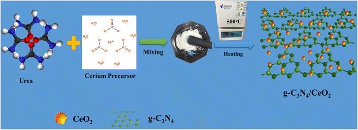
Cerium(III) nitrate hexahydrate (Sigma Aldrich), urea (CH4N2O), deionized water, and ethanol (C2H5OH) solution were purchased from DAEJUNG Co. Ltd, South Korea. All commercial chemicals were used without any further purification. The preparation of g-C3N4 and the binary nanostructured g-C3N4/CeO2 photocatalyst was done through a facile thermal decomposition method. 5 grams of urea were decomposed at 500 °C for 8 h. To synthesize CeO2, cerium(III) nitrate hexahydrate was ground, maintained at 500 °C for 8 h, washed and dried. The binary nanostructured g-C3N4/CeO2 photocatalyst was synthesized by grinding of urea and ceria precursors (1![[thin space (1/6-em)]](https://www.rsc.org/images/entities/char_2009.gif) :
:![[thin space (1/6-em)]](https://www.rsc.org/images/entities/char_2009.gif) 1), processed with the same procedure as CeO2 synthesis, washed, and dried at 100 °C overnight in a oven and denoted as CN/CeO nanostructure (Fig. 1). The materials, characterization and photo/electrochemical test details are discussed in the ESI file.†
1), processed with the same procedure as CeO2 synthesis, washed, and dried at 100 °C overnight in a oven and denoted as CN/CeO nanostructure (Fig. 1). The materials, characterization and photo/electrochemical test details are discussed in the ESI file.†
The structural properties of the synthesized materials were analyzed using powder X-ray diffraction (XRD) with CuKα X-rays (λ = 0.15406 nm) using a Shimadzu XRD-6100 diffractometer. The morphological features were examined using scanning electron microscopy (FESEM, Hitachi S-4800) and high-resolution transmission electron microscopy (HRTEM, Tecnai G2 F20 S-Twin) at an accelerating voltage of 200 kV. The elemental composition was determined using energy dispersive X-ray spectroscopy (EDS) attached to the SEM. The chemical states of the materials were analyzed using Thermo Scientific X-ray photoelectron spectroscopy (XPS) with Al Kα radiation (λ = 1486.6 eV).
The degradation of crystal violet (CV) was studied using the photocatalyst materials. A control experiment was performed in the absence of light to determine the CV equilibrium state on the photocatalyst surface over 30 minutes. For photodegradation experiments under simulated solar light, 50 mL of a 5 ppm CV solution containing 50 mg of the active photocatalyst was placed in a beaker and stirred continuously. The beaker was exposed to simulated solar light (300 W, with a light intensity of 90 mW cm−2) from a light source positioned about 10 cm away from the reactor. The absorption of CV was then measured using a UV-Vis spectrophotometer (Neo-D3117, Neogen).
Photocurrent measurement and electron impedance spectroscopy (EIS) were performed using a three-electrode cell setup. The reference electrode was Ag/AgCl, the counter electrode was a platinum wire, and the working electrode was a fluorine-doped tin oxide (FTO) glass substrate coated with a mixture of the sample, ethanol, and Nafion. The working electrode was prepared by drop-casting the mixture onto the FTO glass and heating it to 90 °C overnight. The photocurrent measurement was conducted under a 300 W Xenon lamp with a light intensity of 90 mW cm−2. EIS was performed over a frequency range of 100 mHz to 200 kHz. All the experiments were carried out in 0.5 M Na2SO4 at ambient temperature on an SP-200 BioLogic workstation.
DFT studies were carried out with Quantum ESPRESSO. The unit cell of g-C3N4 contains 3 carbon atoms and 4 nitrogen atoms and CeO2 contains 4 cerium atoms and 8 oxygen atoms. A (1 × 1 × 1) cell is used for band structure and density of states estimations. The generalized gradient approximation (GGA) with the Perdew–Burke–Ernzerhof (PBE) exchange correlation function was used. 4 × 4 × 4 and 4 × 4 × 1 k-points and a kinetic energy cutoff of 40 Ry and a charge density cutoff of 400 Ry were used for CeO2 and g-C3N4, respectively. For band structure calculation, 8 × 8 × 8 and 8 × 8 × 1 Monkhorst–Pack grids were used to sample the Brillouin zone.
3. Results and discussion
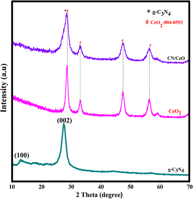
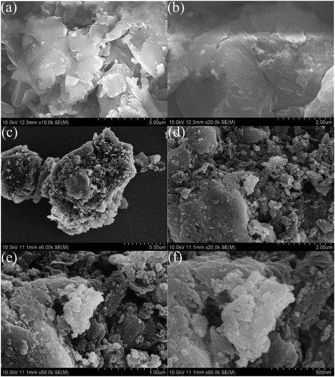
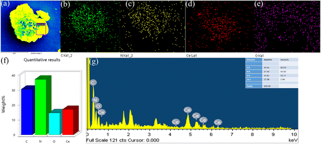
Fig. 2 displays the XRD profiles of g-C3N4, CeO2, and CN/CeO nanostructures. The typical peaks at 12.3 and 27.48°, conforming to (100) and (002), respectively, demonstrate the crystalline nature of the g-C3N4 layered material and confirm the formation of triazine-based C3N4 structures, which align with the ICDD numbers of g-C3N4 (JCPDS-87-1526).26 The XRD profile of bare g-C3N4, as reported by Suter et al.,27 reveals a planar–buckled layer configuration with AB stacking and an interlayer spacing of 0.324 nm, which is confirmed by the presence of a main peak at 27.5°. The XRD pattern of CeO2 shows broad peaks at 2θ, corresponding to (111), (200), (220), and (311), at 28.5°, 33.1°, 47.49°, and 56.4°, respectively, which align with JCPDS no.: 004-0593.28 The XRD pattern of CN/CeO nanostructures shows a major peak at 27.5° 2θ with a broader peak around 28.5° 2θ, attributed to the altered layered features during the pyrolytic impregnation of CeO2 nanosized particles. The presence of CeO2 peaks in the XRD patterns of CN/CeO nanostructures supports the realization of complexes between g-C3N4 and CeO2.Fig. 3 shows the FESEM images of g-C3N4 and CN/CeO nanostructures. The CN/CeO nanostructure has randomly deposited and nanosized particles of CeO2 on the C3N4 sheet surface, which serves as a template for the CeO2 particles during the pyrolysis process, resulting in interfacial contacts. However, CeO2 cannot be seen from the FESEM images due to the nanosized particles and limitations of the SEM instrumentation. This was confirmed by the EDX and mapping results of the CN/CeO nanostructure (Fig. 4). The EDX and mapping results indicate that CeO2 particles are embedded with the g-C3N4 sheets and form a nanostructure.
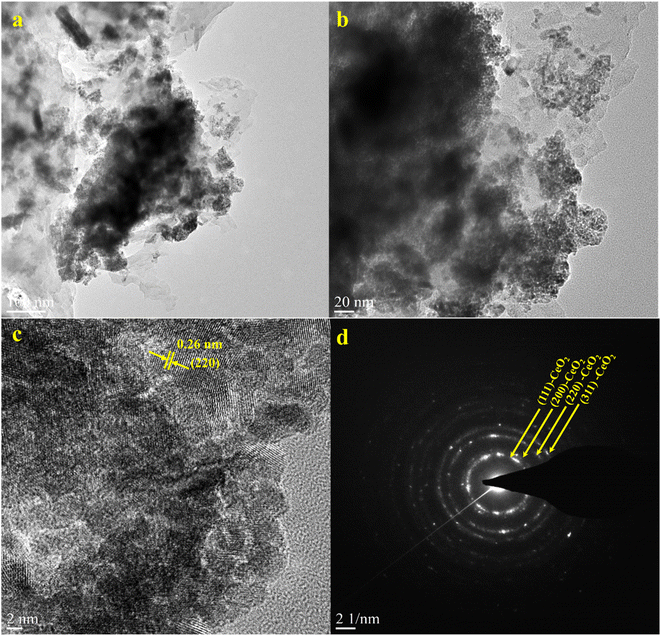
Furthermore, HRTEM analysis was performed on the CN/CeO nanostructure to gain an understanding of the morphological features and CeO2 impregnation on the g-C3N4 surface. The results (Fig. 5(a–c) under high magnification) show that the CeO2 nanosized particles are embedded in the g-C3N4 sheets, around 2–5 nm in size, revealing randomly distributed CeO2 on the g-C3N4 sheets. Fig. 5(c) reveals that the lattice fringe of CeO2 is 0.26 nm, corresponding to the (220) plane. The SAED pattern (Fig. 5(d)) shows a mixed pattern of rings and dots, indicating the coexistence of mixed phases of the materials. The element distribution was also investigated as shown in Fig. 6, which includes HRTEM mapping of HAADF and combined elemental mapping, as well as C, N, Ce, and O element distributions in the CN/CeO nanostructure. Therefore, these findings emphasize the coupling of CeO2 into the g-C3N4 sheets and the presence of both CeO2 and g-C3N4.
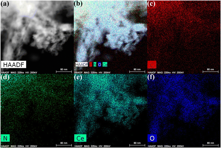 | ||
| Fig. 6 HRTEM-mapping images of (a) HAADF, (b) combined elemental mapping, (c) C, (d) N, (e) Ce, and (f) O elements of the CN/CeO nanostructure. | ||
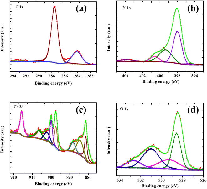
XPS analysis was employed to verify the CN/CeO nanostructure formation and to identify its chemical states. The XPS full survey and typical spectra of C 1s, N 1s, Ce 3d, and O1s are shown in Fig. S1,† with the binding energy values being consistent with previous studies.29 From Fig. 7(a), the binding energies at 284.4 eV and 287.1 eV in the C 1s spectrum are indicative of carbon contaminants or adventitious carbon and sp2 hybridized C atoms, respectively.30–32 The π-excitation indicates the existence of C![[double bond, length as m-dash]](https://www.rsc.org/images/entities/char_e001.gif) N at 292.4 eV. The XPS of the N 1s spectrum, shown in Fig. 7(b), exhibits a main peak at 398 eV (FWHM of 1.89 eV) that is attributed to sp2 mongrelized aromatic C
N at 292.4 eV. The XPS of the N 1s spectrum, shown in Fig. 7(b), exhibits a main peak at 398 eV (FWHM of 1.89 eV) that is attributed to sp2 mongrelized aromatic C![[double bond, length as m-dash]](https://www.rsc.org/images/entities/char_e001.gif) N–C. A band at 400.5 eV is assigned to ternary C–N (–C)–C units, and a weaker band at 404.2 eV is attributed to C–NH–C units.33Fig. 7(c) shows the Ce 3d core-level spectrum reveals the presence of seven coordination numbers of Ce4+ ions and reduced oxygen vacancies, particularly Ce4+-type fluorite structure. The coexistence of Ce3+/Ce4+ can be confirmed through deconvolution of the Ce 3d core-level spectrum. According to the literature, the 3d3/2 and 3d5/2 spin–orbit states are divided into two groups.34 The peaks at 882.2, 888.2, 898.03, 902.38, 907.0, and 916.38 eV are assigned to Ce4+ states, while the remaining peaks at 885 and 900.58 eV belong to Ce3+ states.35Fig. 7(d) shows the O 1s core-level spectrum, where the peaks around 533.01, 531.69, 530.68, and 528.98 eV are allotted to –OH groups, surface oxygen, and O2 in Ce3+ and Ce4+, respectively, which not only reveals the coupling of CeO2 nanosized particles on g-C3N4 sheets and the Ce-CN nanostructure formation, but also discloses the coexistence of metallic and oxidized Ce particles. Additionally, the characteristic triazine-based g-C3N4 sheet structure is confirmed via the C 1s and N 1s core-level bands, which agree well with previous studies.36
N–C. A band at 400.5 eV is assigned to ternary C–N (–C)–C units, and a weaker band at 404.2 eV is attributed to C–NH–C units.33Fig. 7(c) shows the Ce 3d core-level spectrum reveals the presence of seven coordination numbers of Ce4+ ions and reduced oxygen vacancies, particularly Ce4+-type fluorite structure. The coexistence of Ce3+/Ce4+ can be confirmed through deconvolution of the Ce 3d core-level spectrum. According to the literature, the 3d3/2 and 3d5/2 spin–orbit states are divided into two groups.34 The peaks at 882.2, 888.2, 898.03, 902.38, 907.0, and 916.38 eV are assigned to Ce4+ states, while the remaining peaks at 885 and 900.58 eV belong to Ce3+ states.35Fig. 7(d) shows the O 1s core-level spectrum, where the peaks around 533.01, 531.69, 530.68, and 528.98 eV are allotted to –OH groups, surface oxygen, and O2 in Ce3+ and Ce4+, respectively, which not only reveals the coupling of CeO2 nanosized particles on g-C3N4 sheets and the Ce-CN nanostructure formation, but also discloses the coexistence of metallic and oxidized Ce particles. Additionally, the characteristic triazine-based g-C3N4 sheet structure is confirmed via the C 1s and N 1s core-level bands, which agree well with previous studies.36
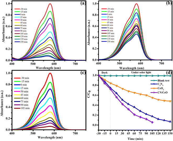
The optical properties of g-C3N4, CeO2, and CN/CeO nanostructures are depicted in Fig. 8. The bandgaps of the samples were estimated from Tauc plots, as illustrated in the inset of Fig. 8. The estimated bandgap of the g-C3N4, CeO2, and CN/CeO nanostructures is 2.64 eV, 3.02 eV and 2.8 eV, respectively. CV dye degradation in an aqueous solution was studied using g-C3N4, CeO2, and CN/CeO nanostructures under simulated solar light (Fig. 9). Fig. 9(a–c) display the UV-vis absorbance of the dye degradation at different time intervals. Fig. 9(d) illustrates the solar-light catalytic activities of the three materials, showing that g-C3N4 and CeO2 demonstrate a weak photoactivity of 82.5% and 45% respectively after 105 min of irradiation. Interestingly, the g-C3N4 photoactivity is significantly improved when combined with CeO2, achieving the highest photoactivity of 94.5% after 105 min. In Fig. 10(a), the kinetics of CV dye degradation over different catalysts are presented, highlighting the superior performance of the CN/CeO nanostructure. The CN/CeO nanostructure exhibits significantly faster kinetics in contrast to g-C3N4. This observation aligns with the findings of Huang et al.,37 who reported that the MB degradation rate constant of the g-C3N4/CeO2 nanocomposite was 12.2 and 3.1 times higher than that of CeO2 and g-C3N4 alone, respectively. This enhanced performance was credited to the synergistic effects at the g-C3N4 and CeO2 interfaces, resulting in improved adsorption capabilities and suitable band positions. Further support for the superior photoactivity of g-C3N4/CeO2 nanocomposites comes from studies by Kesarla et al.38 and She et al.,39 both studies confirmed that g-C3N4/CeO2 nanocomposites exhibited faster photoactivity compared to their individual components, which is consistent with the findings presented in this work. To confirm the stability of the CN/CeO nanostructure, a photocatalytic recycling test was conducted for CV dye, as shown in Fig. 10(b). The photoactivity of CN/CeO remained unchanged after three repeated cycles, indicating that it is remarkably stable during the catalytic process. Fig. S2† depicts the FESEM image of the CN/CeO nanostructure after the cycling test, signifying that the photocatalyst morphology remains consistent with that of the fresh sample.
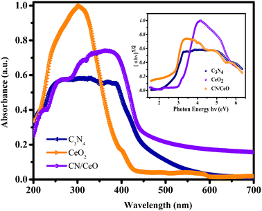 | ||
| Fig. 8 UV-vis absorbance spectra of g-C3N4, CeO2 and CN/CeO nanostructures [inset: their Tauc plots]. | ||
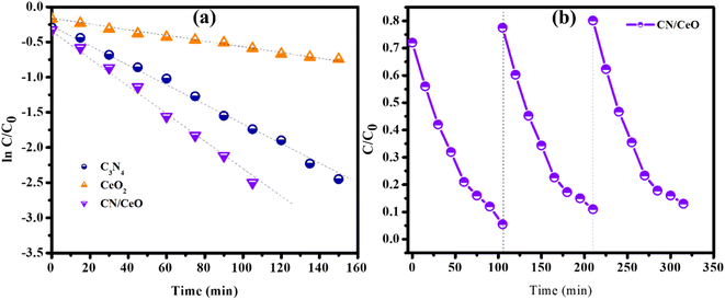 | ||
| Fig. 10 Photocatalytic activity: (a) kinetic plot of photocatalytic degradation of CV dye over different catalysts, and (b) cycling stability results of the CN/CeO nanostructure. | ||
The photoreactions are believed to occur with hydroxyl radicals generated by intricate reactions of photogenerated electrons and holes in aqueous media as follows:40
| h+ + water → OH˙ + H+ | (1) |
| h+ + OH˙ → OH˙ | (2) |
| e− + O2 → O2˙− | (3) |
 | (4) |
 | (5) |
| H2O2 + e− → OH˙ + OH˙ | (6) |
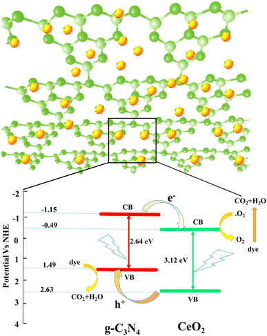
To understand the photoactivities of the CN/CeO nanostructure, the band edge potentials of g-C3N4 and CeO2 were assessed using optical results (Fig. 11).40 Note that this result is consistent with our DFT simulation, as shown in Fig. 12. The estimated band gap energies were used to estimate the following edge potentials: the conduction band potential (ECB) of g-C3N4 and CeO2 is −1.15 eV and −0.49 eV, respectively, and the valence band potential (EVB) is 1.49 eV and 2.63 eV, respectively.41 The standard redox potentials of some radicals can be established in the literature, but they were estimated for ideal conditions, including 25 °C and pH = 7. E(OH˙/H2O), E(O2/O2˙−), and E (OH−/OH˙) are 2.74 V, −0.33 V, and 1.99 V, respectively.42–44 The E(O2/O2˙−) redox potential is −0.16 V for an absorption of 1mol L−1 of O2.44Fig. 11 presents the plausible photoactivity mechanism for the CN/CeO nanostructure, consistent with the band structure from DFT simulation (Fig. 12). The estimated ECB and EVB positions were associated with these redox abilities in an energy level developed for g-C3N4 and CeO2. Based on previous literature, holes could have a significant effect on the performance of reactions eqn (1) and (2).44 Given that the ECB of g-C3N4 exceeds the levels of E0 (O2/O2˙−), it can be anticipated that superoxide radical formation, enabling the reaction in eqn (3), is likely to occur. Analysis of the calculated bandgap energies confirms that the photoreaction proceeds by generating charge carriers within g-C3N4, with electrons subsequently transferring from the ECB of g-C3N4 to CeO2 through the interface. The electrons were detached from the holes obtainable only in the VB of g-C3N4 and reacted according to reactions (3)–(6).44 A similar mechanism has been described in existing literature studies.44–46
 | ||
| Fig. 12 (a) Band structure of CeO2, (b) band structure of g-C3N4, and (c) conduction and valence bands of CeO2 and g-C3N4. | ||
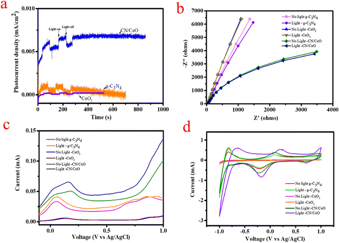
The text describes the results of a study comparing the photocurrent response of three different electrode materials: g-C3N4, CeO2, and CN/CeO. The I–t curves in Fig. 13(a) show that the CN/CeO nanostructure exhibits a higher photocurrent density compared to g-C3N4 and CeO2, with a sharp response and decrease in photocurrent density under light on/off conditions. This result indicates that the CN/CeO nanostructure has a better photoresponse compared to bare g-C3N4 and CeO2. The improvement in photocurrent density is supposed to be due to the synergistic effect between g-C3N4 and CeO2 in the CN/CeO nanostructure, which enhances charge migration and improves carrier separation efficiency.
The text describes the results of an EIS analysis conducted to evaluate the efficiency of charge transfer and blocking the recombination of e−/h+ pairs. The results, shown in Fig. 13(b), with and without light, indicate that the CN/CeO nanostructure has a smaller half circle diameter in the EIS plot compared to bare g-C3N4 and CeO2, indicating improved efficiency in charge transport and rapid interfacial charge transfer. These results are consistent with the enriched photoactivity of the CN/CeO nanostructure, which is believed to be due to the rapid electron transfer kinetics and active separation of photoinduced e−/h+ pairs. When subjected to light irradiation, the CN/CeO nanostructure showed a decreased curvature in the EIS spectra, suggesting that the photon passes through the electrode with minimal resistance. As a result, the CN/CeO nanostructure is considered a promising photoelectrode for water splitting applications.
LSV measurements were performed using an electrochemical workstation, both with light-chopping and in the absence of light. The graph of photocurrent versus bias voltage was plotted from 0 to 1 V with respect to Ag/AgCl, using 0.5 M Na2SO4 as the reference electrode. Fig. 13(c) displays the results of the LSV experiments, which reinforce the findings of this study. The results indicate that the photocurrent of the CN/CeO nanostructure was higher as compare to g-C3N4 and CeO2. This higher current density demonstrates improved ability for electron/hole separation and enhances photocatalytic performance. The j–t and LSV results support the charge transfer dynamics at the interface of g-C3N4 and CeO2 nanosized particles. The smaller bandgap and improved charge transfer dynamics result in a higher photocurrent response in the CN/CeO nanostructure. Additionally, the positive potential response suggests that the OER is favored during LSV measurement, attributed to the high photocurrent efficiency and the OER of the CN/CeO nanostructure. This is a significant advancement in PEC studies. Fig. 13(d) also shows CV curves recorded both under light and without light. These results demonstrate that the CN/CeO nanostructure has photoresponsive behavior, making it a promising candidate for water splitting applications. This suggests that the crystalline CeO2 nanosized particles have a more pronounced photoresponse compared to bare g-C3N4, thanks to the quantum size effect of CeO2.
Fig. 14 illustrates BET surface area isotherms and the corresponding pore size distribution curves for the synthesized g-C3N4, CeO2, and CN/CeO nanostructure samples. These analyses are understanding the textural properties and porosity of the materials, which are critical factors influencing their catalytic performance. The BET surface area measurements reveal distinct characteristics for each material: CeO2 demonstrates a notably surface area of 69 m2 g−1, and the CN/CeO nanostructure displays the highest BET surface area of 81 m2 g−1. Notably, the surface area of the CN/CeO nanostructure surpasses that of its individual constituents, suggesting the emergence of a unique textural structure. Furthermore, the pore size analysis indicates a significant difference between g-C3N4 and the CN/CeO nanostructure. g-C3N4 exhibits a larger pore size of 34 nm, whereas the CN/CeO nanostructure features a relatively smaller pore size of 23 nm. This disparity in pore size distribution is indicative of structural changes that occur during the formation of the composite. The substantial increase in the BET surface area in the CN/CeO nanostructure can be attributed to the creation of a 2D/0D architecture, likely composed of nanosized CeO2 interconnected with 2D stacked layers of g-C3N4. This intricate 2D/0D structural arrangement enhances the charge-transfer dynamics at the interface between the layered g-C3N4 and CeO2 components. Specifically, the 2D g-C3N4 layers serve as efficient platforms for light absorption and charge generation, while the 0D CeO2 nano-sized particles provide active sites for charge transfer and redox reactions. The intimate coupling of these two materials within the CN/CeO nanostructure leads to an enhanced catalytic activity. The increased surface area and modified pore size distribution contribute to a higher accessibility of reactants to active sites and a more favorable environment for catalytic reactions to occur. Therefore, the BET surface area analysis and pore size distribution data underscore the significant structural advantages shown by the CN/CeO nanostructure. The unique 2D/0D architecture promotes efficient charge-transfer dynamics in the interfacial region of g-C3N4 and CeO2, ultimately enhancing the catalytic activity of the composite material.
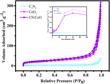 | ||
| Fig. 14 N2 adsorption–desorption isotherm of g-C3N4, CeO2, and CN/CeO nanostructures [inset: their pore size distribution curves]. | ||
4. Conclusion
A method was developed to create g-C3N4-based photocatalysts with randomly distributed CeO2 nanosized particles on g-C3N4 sheets. The CN/CeO nanostructure showed better photocatalytic activity, with 94.5% degradation of CV dye under simulated solar light in 105 min, linked to bare g-C3N4 (82.5%) and CeO2 (45%). The CN/CeO nanostructure also showed improved photoresponse compared to bare g-C3N4, due to the improved separation of photoinduced e−/h+ pairs at the interface between g-C3N4 and CeO2. Furthermore, the photoresponse of the CN/CeO nanostructure is remarkable, so it could a potential photoelectrode in energy conversion applications.Conflicts of interest
The authors declare no competing financial interest.Acknowledgements
Nguyen To Hoai and Nam Nguyen Dang express their gratitude to all the valuable support from Duy Tan University, which is going to celebrate its 30th anniversary of establishment (Nov. 11, 1994–Nov. 11, 2024) towards “Integral, Sustainable and Stable Development” and supported by the National Research Foundation (NRF) of Korea (RS-2023-00280665).References
- F. He, Z. Wang, Y. Li, S. Peng and B. Liu, The nonmetal modulation of composition and morphology of g-C3N4-based photocatalysts, Appl. Catal., B, 2020, 269, 118828 CrossRef CAS.
- World Health Organization, Potable Reuse: Guidance for Producing Safe Drinking-Water, World Health Organization, 2017 Search PubMed.
- T. O. Ajiboye, O. A. Oyewo and D. C. Onwudiwe, Simultaneous removal of organics and heavy metals from industrial wastewater: A review, Chemosphere, 2021, 262, 128379 CrossRef CAS PubMed.
- Y. Chen, D. Tang, Z. Wang, W. Li, M. Yin, Q. Yang, Y. Zhou, K. Zhang, T. Kan and L. Zhou, Z-scheme g-C3N4/Fe2O3 for efficient photo-oxidation of benzylamine under mild conditions, Semicond. Sci. Technol., 2021, 36, 075004 CrossRef CAS.
- X. Yao, X. Jiang, D. Zhang, S. Lu, M. Wang, S. Pan, X. Pu, J. Liu and P. Cai, Achieving improved full-spectrum responsive 0D/3D CuWO4/BiOBr:Yb3+, Er3+ photocatalyst with synergetic effects of up-conversion, photothermal effect and direct Z-scheme heterojunction, J. Colloid Interface Sci., 2023, 64, 95–106 CrossRef PubMed.
- D. Zhang, X. Liu, S. Wang, B. Fan, Z. Shao, C. Su and X. Pu, Enhanced charges separation to improve hydrogen production efficiency by organic piezoelectric film polarization, J. Alloys Compd., 2021, 869, 159390 CrossRef CAS.
- P. Su, D. Kong, H. Zhao, S. Li, D. Zhang, X. Pu, C. Su and P. Cai, SnFe2O4/ZnIn2S4/PVDF piezophotocatalyst with improved photocatalytic hydrogen production by synergetic effects of heterojunction and piezoelectricity, Appl. Catal., B, 2023, 12, 1685–1700 CAS.
- D. Zhang, R. Zhang, J. Liu, X. Pu and P. Cai, 3D/2D ZnIn2S4/BiFeO3 as S-scheme heterojunction photocatalyst for boosted visible-light hydrogen evolution, J. Am. Ceram. Soc., 2023, 106, 4785–4793 CrossRef CAS.
- M. M. Kandy, Carbon-based photocatalysts for enhanced photocatalytic reduction of CO2 to solar fuels, Sustainable Energy Fuels, 2020, 4, 469–484 RSC.
- Y. Fan, C. He and Y. Li, Iron oxide clusters on g-C3N4 promote the electron–hole separation in photo-Fenton reaction for efficient degradation of wastewater, Chem. Pap., 2022, 76, 7553–7563 CrossRef CAS.
- Y. Lui, Y. Gong, X. Cui, H. Yu, W. Qin, X. Cui and M. Huo, Synthesis of O-doped C3N4 decorated with C3N4 quantum dots: Construction of a homo junction photocatalyst for the enhanced photocatalytic degradation of tetracycline, J. Taiwan Inst. Chem. Eng., 2022, 138, 104457 CrossRef.
- Y. Zhong, W. Chen, S. Yu, Z. Xie, S. Wei and Y. Zhou, CdSe quantum dots/g-C3N4 heterostructure for efficient H2 production under visible light irradiation, ACS Omega, 2018, 3, 17762–17769 CrossRef CAS PubMed.
- Z. Lui, Z. Zhang, D. Xie, X. Guan, F. Wang and B. Xue, Preparation of graphitic carbon nitride g-C3N4-HMCM-22 composite catalysts and enhanced para-selectivity in m-xylene isomerization, Chem. Pap., 2022, 76, 1875–1884 CrossRef.
- M. Qui, W. Xu, S. Chen, Z. Jia, Y. Li, J. He, L. Wang, J. Lei, C. Lui and J. Liu, A novel adsorptive and photocatalytic system for dye degradation using ZIF-8 derived carbon (ZIF-C)-modified graphene oxide nanosheets, J. Taiwan Inst. Chem. Eng., 2023, 143, 104674 CrossRef.
- D. A. F. Gonçalves, M. V. B. Pinheiro, K. Krambrock, R. R. Resende, B. R. L. Galvão and E. Lorençon, Oxidative desulfurization of dibenzothiophene over highly dispersed Mo-doped graphitic carbon nitride, Chem. Pap., 2022, 76, 3401–3412 CrossRef.
- H. Venkatesvaran, S. Balu, B. S. Tsai and T. C. K. Yang, Construction of Z-scheme heterojunction based on BiOBr-nanoflakes embedded sulfonic-acid-functionalized g-C3N4 for enhanced photocatalytic removal of hazardous pollutants in aqueous media, J. Taiwan Inst. Chem. Eng., 2023, 142, 104637 CrossRef CAS.
- A. Kumar, A. Kumar, G. Sharma, M. Naushad, F. J. Stadler, A. A. Ghfar, P. Dhiman and R. V. Saini, Sustainable nano-hybrids of magnetic biochar supported g-C3N4/FeVO4 for solar powered degradation of noxious pollutants- Synergism of adsorption, photocatalysis & photo-ozonation, J. Cleaner Prod., 2017, 165, 431–451 CrossRef CAS.
- N. Zhang, L. Wen, J. Yan and Y. Liu, Dye-sensitized graphitic carbon nitride (g-C3N4) for photocatalysis: a brief review, Chem. Pap., 2020, 74, 389–406 CrossRef CAS.
- M. H. Foghani, O. Tavakoli, M. J. Parnian and R. Zarghami, Enhanced visible light photocatalytic CO2 reduction over direct Z-scheme heterojunction Cu/P co-doped g-C3N4@TiO2 photocatalyst, Chem. Pap., 2022, 76, 3459–3469 CrossRef CAS.
- J. T. Lee, S. W. Lee and M. Y. Wey, S-scheme g-C3N4/ZnO heterojunction photocatalyst with enhanced photodegradation of azo dye, J. Taiwan Inst. Chem. Eng., 2022, 134, 104357 CrossRef CAS.
- M. C. Maridevaru, A. H. Naceruddin, B. Aljafari and S. Anandan, Low-frequency acoustic irradiation coupled photocatalytic degradation of dye pollutant using LaNi0.5Co0.5O3/g-C3N4 nanocatalyst, J. Taiwan Inst. Chem. Eng., 2022, 140, 104570 CrossRef CAS.
- N. Iqbal, A. Afzal, I. Khan, M. S. Khan and A. Qurashi, Molybdenum impregnated g-C3N4 nanotubes as potentially active photocatalyst for renewable energy applications, Sci. Rep., 2021, 11, 16886 CrossRef CAS PubMed.
- J. Rashid, N. Parveen, A. Iqbal, S. U. Awan, N. Iqbal, S. H. Talib, N. Hussain, B. Akram, A. Ulhaq, B. Ahmed and M. Xu, Facile synthesis of g-C3N4(0.94)/CeO2(0.05)/Fe3O4(0.01) nanosheets for DFT supported visible photocatalysis of 2-chlorophenol, Sci. Rep., 2019, 9, 10202 CrossRef PubMed.
- M. Humayun, Z. Hu, A. Khan, W. Cheng, Y. Yuan, Z. Zheng, Q. Fu and W. Luo, Highly efficient degradation of 2,4-dichlorophenol over CeO2/g-C3N4 composites under visible-light irradiation: Detailed reaction pathway and mechanism, J. Hazard. Mater., 2019, 364, 635–644 CrossRef CAS PubMed.
- A. Kumar, S. K. Sharma, G. Sharma, M. Naushad and F. J. Stadler, CeO2/g-C3N4/V2O5 ternary nano hetero-structures decorated with CQDs for enhanced photo-reduction capabilities under different light sources: Dual Z-scheme mechanism, J. Alloys Compd., 2020, 838, 155692 CrossRef CAS.
- G. Murali, S. P. Vattikuti, Y. K. Kshetri, H. Lee, J. K. R. Modigunta, C. S. Reddy, S. Park, S. Lee, B. Poornaprakash, H. Lee and Y. H. Park, Near-infrared-activated Z-scheme NaYF4:Yb/Tm@Ag3PO4/Ag@g-C3N4 photocatalyst for enhanced H2 evolution under simulated solar light irradiation, Chem. Eng. J., 2021, 421, 129687 CrossRef CAS.
- T. Suter, V. Brázdová, K. McColl, T. S. Miller, H. Nagashima, E. Salvadori, A. Sella, C. A. Howard, C. W. Kay, F. Corà and P. F. McMillan, Synthesis, structure and electronic properties of graphitic carbon nitride films, J. Phys. Chem. C, 2018, 122, 25183–25194 CrossRef CAS.
- S. N. Matussin, F. Khan, M. H. Harunsani, Y. M. Kim and M. M. Khan, Effect of Pd-doping concentrations on the photocatalytic, photoelectrochemical, and photoantibacterial properties of CeO2, Catalysts, 2023, 13, 96 CrossRef CAS.
- W. Zhao, T. She, J. Zhang, G. Wang, S. Zhang, W. Wei, G. Yang, L. Zhang, D. Xia, Z. Cheng and H. Huang, A novel Z-scheme CeO2/g-C3N4 heterojunction photocatalyst for degradation of bisphenol A and hydrogen evolution and insight of the photocatalysis mechanism, J. Mater. Sci. Technol., 2021, 85, 18–29 CrossRef CAS.
- S. V. P. Vattikuti, A. K. R. Police, J. Shim and C. Byon, In situ fabrication of the Bi2O3–V2O5 hybrid embedded with graphitic carbon nitride nanosheets: Oxygen vacancies mediated enhanced visible-light–driven photocatalytic degradation of organic pollutants and hydrogen evolution, Appl. Surf. Sci., 2018, 447, 740–756 CrossRef CAS.
- X. She, H. Xu, H. Wang, J. Xia, Y. Song, J. Yan, Y. Xu, Q. Zhang, D. Du and H. Li, Controllable synthesis of CeO2/g-C3N4 composites and their applications in the environment, Dalton Trans., 2015, 44, 7021–7031 RSC.
- S. V. P. Vattikuti, P. A. K. Reddy, J. Shim and C. Byon, Visible-light-driven photocatalytic activity of SnO2–ZnO quantum dots anchored on g-C3N4 nanosheets for photocatalytic pollutant degradation and H2 production, ACS Omega, 2018, 3, 7587–7602 CrossRef CAS PubMed.
- H. Jiang, X. Li, S. Chen, H. Wang and P. Huo, g-C3N4 quantum dots-modified mesoporous CeO2 composite photocatalyst for enhanced CO2 photoreduction, J. Mater. Sci.: Mater. Electron., 2020, 31, 20495–20512 CrossRef.
- P. Burroughs, A. Hamnett, A. F. Orchard and G. Thornton, Satellitestructure in the X-ray photoelectron spectra of some binary and mixed oxides of lanthanum and cerium, J. Chem. Soc., Dalton Trans., 1976, 17, 1686–1698 RSC.
- M. K. Kesarlaa, M. O. Fuentez-Torresb, M. A. Alcudia-Ramosb, F. Ortiz-Chic, C. G. Espinosa-Gonzálezc, M. Alemand, J. G. Torres-Torresb and S. Godavarthic, Synthesis of g-C3N4/N-doped CeO2 composite for photocatalytic degradation of an herbicide, J. Mater. Res. Technol., 2019, 8, 1628–1635 CrossRef.
- R. Ma, S. Zhang, L. Li, P. Gu, T. Wen, A. Khan, S. Li, B. Li, S. Wang and X. Wang, Enhanced visible-light-induced photoactivity of type-II CeO2/g-C3N4 nanosheet toward organic pollutants degradation, ACS Sustainable Chem. Eng., 2019, 7, 9699–9708 CrossRef CAS.
- L. Huang, Y. Li, H. Xu, Y. Xu, J. Xia, K. Wang, H. Li and X. Cheng, Synthesis and characterization of CeO2/g-C3N4 composites with enhanced visible-light photocatalytic activity, RSC Adv., 2013, 3, 22269–22279 RSC.
- M. K. Kesarla, M. O. Fuentez-Torres, M. A. Alcudia-Ramos, F. Ortiz-Chic, C. G. Espinosa-González, M. Aleman, J. G. Torres-Torres and S. Godavarthi, Synthesis of g-C3N4/N-doped CeO2 composite for photocatalytic degradation of an herbicide, J. Mater. Res. Technol., 2019, 8, 1628–1635 CrossRef CAS.
- X. She, H. Xu, H. Wang, J. Xia, Y. Song, J. Yan, Y. Xu, Q. Zhang, D. Du and H. Li, Controllable synthesis of CeO2/g-C3N4 composites and their applications in the environment, Dalton Trans., 2015, 44, 7021–7031 RSC.
- Z. Huang, L. Li, Z. Li, H. Li and J. Wu, Synthesis of novel kaolin-supported g-C3N4/CeO2 composites with enhanced photocatalytic removal of ciprofloxacin, Materials, 2020, 13, 3811 CrossRef CAS PubMed.
- W. J. Ong, L. L. Tan, Y. H. Ng, S. T. Yong and S. P. Chai, Graphitic carbon nitride (g-C3N4)-based photocatalysts for artificial photosynthesis and environmental remediation: Are we a step closer to achieving sustainability?, Chem. Rev., 2016, 116, 7159–7329 CrossRef CAS PubMed.
- K. Li, X. Zeng, S. Gao, L. Ma, Q. Wang, H. Xu, Z. Wang, B. Huang, Y. Dai and J. Lu, Ultrasonic-assisted pyrolyzation fabrication of reduced SnO2-x/g-C3N4 heterojunctions: enhance photoelectrochemical and photocatalytic activity under visible LED light irradiation, Nano Res., 2016, 9, 1969–1982 CrossRef CAS.
- P. M. Wood, The potential diagram for oxygen at pH 7, Biochem. J., 1988, 253, 287–289 CrossRef CAS PubMed.
- P. Prausa, L. Svoboda, R. Dvorskýc and M. Reli, Nanocomposites of SnO2 and g-C3N4: Preparation, characterization and photocatalysis under visible LED irradiation, Ceram. Int., 2018, 44, 3837–3846 CrossRef.
- B. Tao and Z. Yan, In-situ synthesis of highly efficient visible light driven stannic oxide/graphitic carbon nitride heterostructured photocatalysts, J. Colloid Interface Sci., 2016, 480, 118–125 CrossRef CAS PubMed.
- Y. Zang, L. Li, X. Li, R. Lin and G. Li, Synergistic collaboration of g-C3N4/SnO2 composites for enhanced visible-light photocatalytic activity, Chem. Eng. J., 2014, 246, 277–286 CrossRef CAS.
Footnote |
| † Electronic supplementary information (ESI) available. See DOI: https://doi.org/10.1039/d3na00774j |
| This journal is © The Royal Society of Chemistry 2023 |

