
Indirect bandgap MoSe2 resonators for light-emitting nanophotonics†
Bogdan R.
Borodin
 *a,
Fedor A.
Benimetskiy
b,
Valery Yu.
Davydov
a,
Ilya A.
Eliseyev
a,
Alexander N.
Smirnov
a,
Dmitry A.
Pidgayko
b,
Sergey I.
Lepeshov
b,
Andrey A.
Bogdanov
b and
Prokhor A.
Alekseev
a
*a,
Fedor A.
Benimetskiy
b,
Valery Yu.
Davydov
a,
Ilya A.
Eliseyev
a,
Alexander N.
Smirnov
a,
Dmitry A.
Pidgayko
b,
Sergey I.
Lepeshov
b,
Andrey A.
Bogdanov
b and
Prokhor A.
Alekseev
a
aIoffe Institute, Saint Petersburg, 194021, Russia. E-mail: brborodin@gmail.com
bITMO University, Saint Petersburg, 197101, Russia
First published on 16th January 2023
Abstract
Transition metal dichalcogenides (TMDs) are promising for new generation nanophotonics due to their unique optical properties. However, in contrast to direct bandgap TMD monolayers, bulk samples have an indirect bandgap that restricts their application as light emitters. On the other hand, the high refractive index of these materials allows for effective light trapping and the creation of high-Q resonators. In this work, a method for the nanofabrication of microcavities from indirect TMD multilayer flakes, which makes it possible to achieve pronounced resonant photoluminescence enhancement due to the cavity modes, is proposed. Whispering gallery mode (WGM) resonators are fabricated from bulk indirect MoSe2 using resistless scanning probe lithography. A micro-photoluminescence (μ-PL) investigation revealed the WGM spectra of the resonators with an enhancement factor up to 100. The characteristic features of WGMs are clearly seen from the scattering experiments which are in agreement with the results of numerical simulations. It is shown that the PL spectra in the fabricated microcavities are contributed by two mechanisms demonstrating different temperature dependences. The indirect PL, which is quenched with the temperature decrease, and the direct PL which almost does not depend on the temperature. The results of the work show that the suggested approach has great prospects in nanophotonics.
New conceptsBulk transition metal dichalcogenides (TMDs) have an extremely high refractive index (∼5) in the visible and IR spectral ranges. It makes them an ideal medium for nanophotonic structures. However, due to an indirect bandgap, the main attention for the application of TMDs in the field of nanophotonics is paid to the creation of dielectric nanophotonic structures for light absorption or low-loss nanophotonics. To date, there are practically no studies devoted to light-emitting TMD nanophotonic structures. Here we introduce a novel type of stand-alone TMD nanocavity as a source of excitonic photoluminescence. Disk whispering-gallery-mode optical nanoresonators were made of bulk indirect bandgap MoSe2. Brand new frictional probe lithography was used to fabricate nanoresonators so as not to disturb the pristine properties of the TMD, which are highly sensitive to any contamination or chemical treatment. The obtained nanoresonators demonstrate strongly enhanced (by two orders of magnitude) photoluminescence in the range of 850 to 1050 nm. Peak positions can be tuned by varying the nanocavity diameter. This work demonstrates a new approach to the fabrication of light-emitting nanophotonic devices from indirect bandgap TMDs and opens up many opportunities for further research. |
1 Introduction
Since the discovery of graphene in 2004,1 layered materials have become one of the most booming topics in many fields, such as materials science,2 condensed matter physics,3 optoelectronics,4 and photonics,5etc. The most prospective semiconductive materials seem to be transition metal dichalcogenides (TMDCs). This is due to the unique properties of their monolayers such as extraordinary light absorption,6 large exciton binding energies,7,8 strong and tailoring photoluminescence,9–11 the possibility of creating van der Waals heterostructures,12,13 twisting engineering,14–16etc. Such an active investigation of TMDC monolayers has revived interest in studying the properties of their bulk samples. These materials in their bulk form were actively studied back in the 1970s.17–20 However, today, researchers can take a fresh look at their bulk properties using the progress that has been made in understanding physical phenomena and the best modern equipment that allows researchers to look deeper at known properties and to find new ones. Most recent studies have revealed many new outstanding properties of multilayered TMDCs, such as their giant optical anisotropy,21 polarizing effects,22 anapole–exciton polaritons,23 exciton–plasmon–polaritons,24 exciton–polariton transport,25 second harmonic generation,26etc. All the above-mentioned properties make these materials a perfect candidate for a variety of nanophotonic applications including lasers,27,28 waveguides,25,29,30 high harmonic generation,30–32 bound states in the continuum,33,34etc.However, there is a significant obstacle in the way of the implementation of light-emitting nanophotonic devices. Multilayered TMDCs have an indirect bandgap that results in negligible photoluminescence (PL).35 To use some of the unique properties of TMDCs, many researchers integrate direct bandgap TMDC monolayers into external photonic circuits/resonators as a source of excitonic photoluminescence.27,36–38 Because of their thickness, stand-alone monolayers cannot be used to fabricate waveguides or resonators for the visible and near-IR ranges. That requires forming photonic circuits and exciton/PL sources using various technological processes and different materials. All this considerably complicates the on-chip integration of TMDC materials. Another way to solve this problem is to use the Purcell effect to enhance the PL intensity of multilayered TMDCs.39–41 This approach was successfully used to enhance the light emission of Si in optical cavities.42–45 Although due to the strong absorption of free charge carriers in Si, the effect was not game-changing.46–49 Owing to an extremely high refractive index in the visible and near-IR ranges (n ≈ 4–5),50,51 high-Q nanocavities with a strong Purcell effect and enhanced emissivity might be made from bulk TMDCs (the principle is illustrated in Fig. 1).52
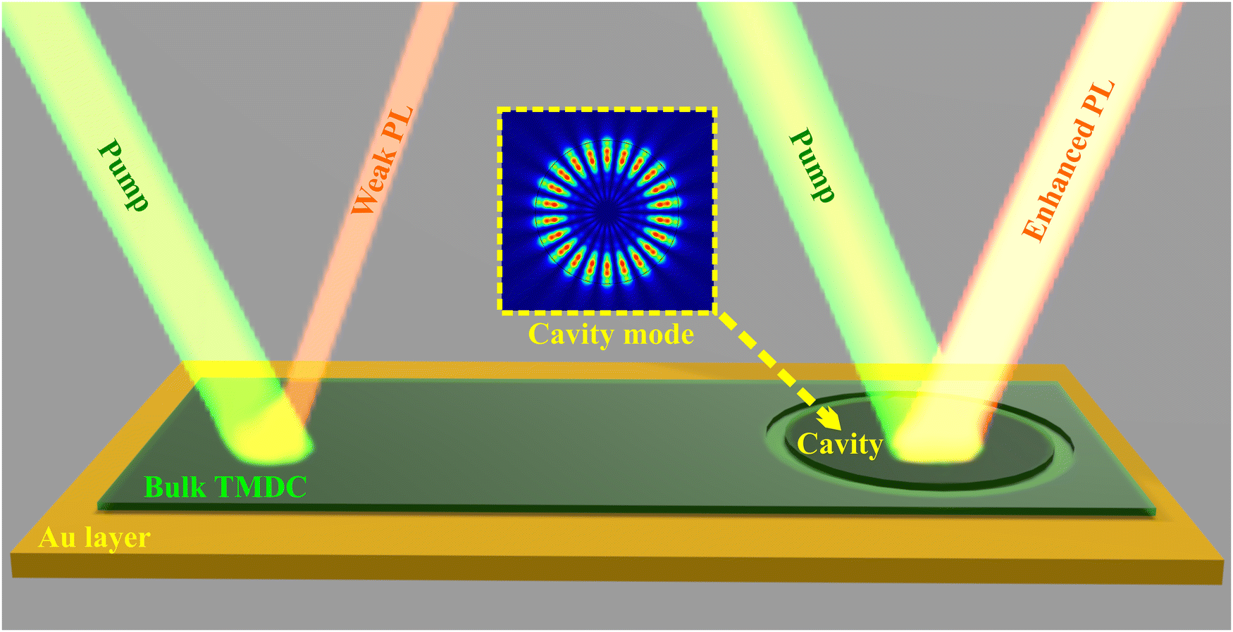 | ||
| Fig. 1 Principal scheme of PL enhancement in cavities made of indirect bandgap TMDCs. Owing to the indirect bandgap, the PL signal from the bulk flakes is weak. However, it can be enhanced by a cavity. | ||
In this work, we create disk whispering-gallery mode (WGM) optical nanoresonators from multilayered MoSe2. Resistless mechanical probe lithography was used to fabricate the nanoresonators so as not to disturb the pristine properties of the TMDCs, which are highly sensitive to any contamination or chemical treatment.53–55 The obtained nanocavities demonstrate strongly enhanced (by two orders of magnitude) photoluminescence in the range of 850 to 1050 nm. The spectral features correspond to WGM resonances, which were confirmed by numerical simulations and scattering experiments. The results of the work allow the introduction of novel types of standalone TMDC nano- and microcavities as sources of excitonic photoluminescence for on-chip integrated nanophotonic circuits.
2 Experimental
2.1 Sample preparation
Thin-film MoSe2 samples were fabricated by mechanical exfoliation with adhesive tape (blue tape, Nitto) from a commercial bulk crystal (obtained from HQ Graphene, Netherlands) on top of the Au/Si substrate.2.2 Cavities creation
The cavities were created by resistless frictional mechanical probe lithography. To perform the procedure, we used a Ntegra Aura (NT-MDT) atomic force microscope using DCP (NT-MDT) probes with a curvature radius of 100 nm and a spring constant of 30–85 N m−1. The multi-pass frictional approach was used to prevent defect formation. The force was about 10 μN, and the number of passes amounted to 200 for each resonator. Detailed information on this approach and the cavity creation process is available in our previous work.56,572.3 Micro-photoluminescence (μ-PL) investigation
The optical properties of the structures were investigated by measuring the PL spectra. For these experiments, a multi-functional optical complex Horiba LabRAM HREvo UV-VIS-NIR-Open equipped with a confocal microscope was used. The spectra were obtained with a spectral resolution of 3 cm−1 using a 600 g mm−1 grating. We used an Olympus MPLN100× objective lens (NA = 0.9) to obtain information from an area with a diameter of 1 μm. Apart from local measurements, PL mapping with a spatial resolution of 0.5 μm was performed at the same setup using a motorized table. The measurements were performed with continuous-wave (cw) excitation using the 532 nm laser line of a Nd:YAG laser (Laser Quantum Torus). To prevent damage to the structures, the incident laser power was limited to 1 mW.2.4 Scattering experiments
The microdisks were illuminated with white polarised light (Ocean Optics HL-2000-HP in combination with linear polariser) at an incidence angle of 65 degrees with a low-aperture lens Mitutoyo Plan Apo NIR 10 × 0.26 NA. The radiation scattered by the disks is collected using the Mitutoyo Plan Apo NIR 50 × 0.65 NA which was analysed on a Horiba LabRAM HR 800 UV-VIS-NIR spectrometer. The numerical apertures of the lenses and the angle of incidence are chosen so that the pump does not pass through the collection channel.3 Results and discussion
3.1 Fabrication of nanocavities
An experimental structure consisting of thin MoSe2 flakes was transferred onto a Si substrate covered with 50 nm of gold. MoSe2 flakes were obtained by micro-mechanical exfoliation and were transferred using a standard approach (i.e., scotch-tape method) without using PDMS to prevent contamination with the polymer.54Fig. 2a shows the cross-section of the structure used.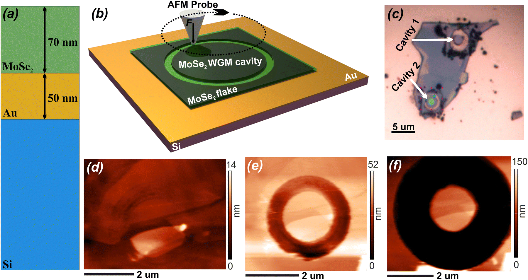 | ||
| Fig. 2 (a) Cross-section of the sample. (b) Scheme of frictional probe lithography of a cavity. (c) Optical image of the MoSe2 flake with two cavities. (d–f) AFM images of the cavity creation process. | ||
To create a cavity, we firstly found a flake of a thickness of about 70–100 nm that is sufficient to accommodate the WGMs. Then we used frictional scanning probe lithography (f-SPL) to fabricate the cavities.57 The scheme of the f-SPL is shown in Fig. 2b. f-SPL is a resistless method of lithography based on the mechanical influence of an atomic force microscopy (AFM) probe on the sample surface to remove the material (mechanical-SPL). However, while m-SPL conventionally uses high pressure to deepen the lithographic patterns (“cutting” regime), f-SPL consists of consequent repetitions of the lithographic patterns with a small amount of pressure on the sample. Thus, during f-SPL, the material is gradually rubbed out from the surface. This approach allows the avoidance of cantilever twisting that prevents the formation of artifacts and makes it possible to maintain high resolution even in the case of thick samples. Fig. 2c shows an optical image of the processed flake. It can be seen that two circular cavities are formed from the flake, and the removed material is nearby. Fig. 2d–f demonstrates the AFM images of the cavity creation process. The first is a relatively flat surface of the flake. The second is the surface with a half-thickness trench. The third is the fully separated cavity and the full-thickness trench. The optical properties of such cavities were studied by μ-PL and dark-field spectroscopy.
3.2 Optical properties of nanocavities
As discussed in the introduction, TMDs have many peculiar properties that can appear in the optical response of such structures. However, a combination of photoluminescence and scattering investigations is a reliable method to determine the nature of the observed features. The shape of the spectra and the peak-to-peak distance are strong evidence of resonant phenomena, whether they are WGM or Mie resonances. Thus, the optical properties of the cavities were studied using micro-PL and dark-field spectroscopy. Fig. 3 demonstrates the results of the PL and experimental dark-field (DF) spectroscopy measurements supported by DF numerical calculations. In the μ-PL spectrum, we observe a series of peaks (see Fig. 3a), which may potentially originate from the whispering gallery mode resonance. Further, we carry out the DF spectroscopy of the cavity previously exposed by the PL measurements. Since the DF spectroscopy deals only with the optical resonances of a cavity, it allows us to unambiguously identify whether the PL peaks have a resonant nature or not. The results are shown in Fig. 3(b, red curve). One can see that we observe the resonant features in the spectral regions similar to those that we get through PL measurements (Fig. 3a).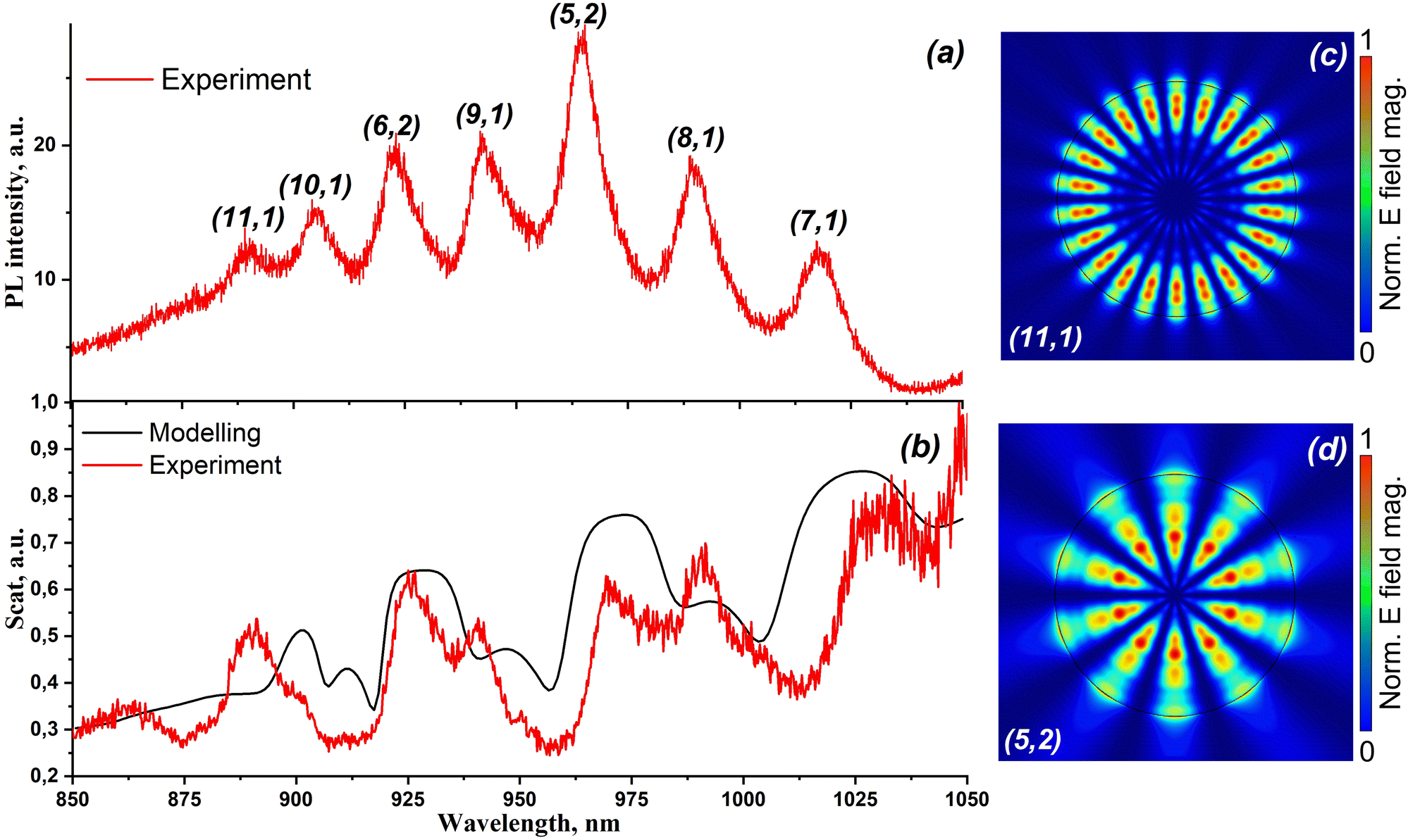 | ||
| Fig. 3 (a) Photoluminescence and (b) dark-field spectra of the cavity for s-polarised incidence. The red curves correspond to the experimental measurements, the black curve represents the numerical calculations. The numbers in brackets represent the azimuthal and radial numbers (M, n) for modes corresponding to the associated peaks. (c and d) Electrical field distribution in the cavity for (11, 1) and (5, 2) modes modeled in COMSOL Multiphysics. | ||
To prove the optical resonance nature of the PL peaks, we prepare comprehensive numerical simulations of optical scattering in COMSOL Multiphysics. We assume a MoSe2 disk on the top of a Si substrate covered by a layer of Au. The permittivities of MoSe2, Si and Au are taken from ref. 18, 58 and 59. The disk diameter is 2.2 μm, the height is 70 nm, and the thickness of the Au layer is 50 nm. To calculate the scattering spectrum, we illuminate the structure by the s-polarised plane wave with the incident angle of 65° and collect the scattered wave in the numerical aperture of 0.65. The results of the numerical calculation of the DF spectrum are presented in Fig. 3(b, black curve). The experimentally obtained DF spectrum is in a good agreement with the numerical one. Based on the resonant behaviour of the DF spectra and the peak-to-peak comparison, we conclude that the PL peaks have an optical resonance nature. Fig. 3c and d demonstrate the electrical field distribution in the cavity for the (11, 1) and (5, 2) modes modeled in COMSOL Multiphysics.
Conventionally, when TMD monolayers are used as light emitters, the external resonator is tuned to the direct exciton transition60–62 (i.e., 780 nm/1.57 eV in the MoSe2 case).9 In our case, we use a bulk TMD layer simultaneously as a resonator and an emitter. Therefore, the absorption of the emitted light is of great importance in our case. Even bulk TMDs have a strong absorbance near the excitonic resonance, while the luminescence is weak.19,63 Thus, to avoid maximum absorption, we should tune our resonators to the long wavelength tail of the photoluminescence.
Fig. 4 shows the μ-PL data for cavities of various diameters. The spectra consist of a series of peaks that are specific for whispering gallery modes. The size variety of the cavities provides different positions of the maxima and enhancement factors. The 2.2 μm diameter cavity exhibits significantly enhanced PL with an enhancement factor of up to 100. Additionally, one can notice that the PL maxima of the cavities are shifted to the long-wavelength region compared to the PL peak of the flake. Such a red-shift of the PL maxima can be explained by the dominant contribution of the cavity modes to the PL in the long-wavelength region (900–1050 nm) and suppression of the cavity radiation due to the significant MoSe2 material losses in the short-wavelength region (800–900 nm). The PL maximum of the bare MoSe2 appears in the highly absorptive wavelength range below 900 nm. Therefore, the cavity modes produce a small PL signal in the short-wavelength region where the absorptive losses are simultaneously resonantly enhanced. For this reason, the disks with smaller diameters of 1.4 and 1.6 μm that have a high-Q resonance at the shorter wavelengths did not show such a strong enhancement.56 Moreover, we created structures of larger diameters (3, 5, and 10 μm). The PL data of these structures are presented in the ESI† in Fig. S1. The 3 μm cavity demonstrates some features related to WGMs.
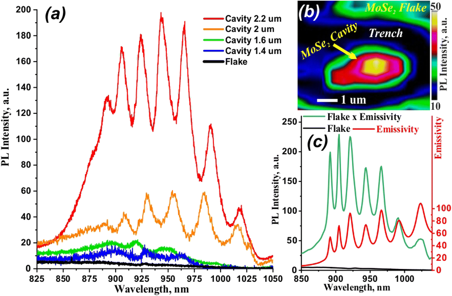 | ||
| Fig. 4 (a) PL spectra of cavities of various diameters. (b) PL mapping of one of the structures. (c) Calculated emissivity of the 2.2 μm cavity (red curve), the flake spectrum (black curve), and the flake spectrum multiplied by the emissivity (green curve). | ||
However, these peaks are significantly weaker than in the 2.2 μm cavity case, and the flake-like PL peak dominates (see Fig. S1, red curve, ESI†). With increasing cavity diameter, all WGM features disappear, and only the unmodified flake photoluminescence remains in the spectra (see Fig. S1, ESI†, purple and blue curves). Such dependence of the PL on the cavity diameter can be explained by competition between the gain and material losses. On one hand, a larger cavity should provide higher enhancement due to the high-quality factor of modes with a higher azimuthal number. On the other hand, a longer light path in larger cavities relates to more intensive absorption by indirect bandgap materials. Consequently, small cavities have low a Q factor but low losses (1.4 and 1.6 μm), large cavities have a high Q factor but high losses (3, 5, and 10 μm), and there is most likely some compromise with satisfying gain and losses (2, and 2.2 μm). Thus, we believe that the 2.2 μm diameter cavity is a compromise between miniature size and enhancement factor (≈100).
The enhanced PL originates from the Purcell effect caused by the whispering gallery modes of the microdisk. The direct evidence of the Purcell effect is the shortening of the lifetime of the excited states. We measured the time-resolved PL for the cavity with the largest enhancement factor (see Fig. 3S in ESI†). Fig. 3S (ESI†) shows the instrument response function (IRF) of the experimental setup and the PL decay curves for the bulk flake and the microcavity with a 2.2 μm diameter, which were measured at 966 nm (see Fig. 4a). The long lifetime part of the IRF curve is associated with the effect of the diffusion tail, which is typical for such types of detectors.64 The full width at half maximum (FWHM) values for the IRF and PL decay curves were extracted from experimental data and are approximately 80 ps. To analyze the measured spectra more precisely, we approximate them with a two-phase exponential decay function. The time constants for the short lifetime region of the curves are tBulk1 = 37 ± 2 ps, tCavity1 = 37 ± 2 ps, tIRF1 = 36 ± 2 ps which are in good agreement with the FWHM values, and the main difference of the measured spectra is observed for the time constants associated with a long lifetime region: tBulk2 = 345 ± 10 ps, tCavity2 = 318 ± 2 ps, tIRF2 = 311 ± 10 ps. Such behavior may indicate a decrease of the PL lifetime due to increasing the local density of the optical states for the cavity, but the time resolution limitation and the effect of the diffusion tail make it difficult to interpret the results.
Furthermore, to estimate the impact of the Purcell effect and to validate our experimental results, we perform numerical calculations of the emissivity of the microdisk in COMSOL Multiphysics.65 In order to calculate the intensity of the emitted field, we utilize the reciprocity theorem. The reciprocity theorem dictates that the electric field intensity emitted by the current distribution is equal to the intensity necessary for excitation of the current distribution. As a consequence, the ability of the cavity to absorb the incident energy matches with its ability to emit. Thus, to estimate the emissivity, it is enough to find the energy absorbed in the microdisk. Fig. 4 (c, red curve) shows the emissivity spectrum of the microdisk with the diameter equal to 2.2 μm. The emissivity is calculated as an integral of the field intensity inside the microdisk. Multiplication of the emissivity and the flake PL spectrum gives the PL of the MoSe2 microdisk. The positions of the peaks obtained in the calculations perfectly match with those that are experimentally measured.
One can notice that conventionally WGM resonators do not emit vertically. However, the presence of defects might serve as a scatterer or antenna, and a finite aperture of the collecting objective provides simultaneous collection in some angle ranges. We can see such defects in our structures (e.g., non-uniform thickness in Fig. 2d). In addition, we have noticed that the PL signals strongly depend on a collection spot. Fig. 4b demonstrates the PL mapping of one of the structures. It can be seen that the PL intensity is not uniformly distributed, and that there are hot spots. So, in our experiments, we chose the spots that demonstrate the maximum PL intensity to record the PL spectra.
3.3 Temperature dependence of photoluminescence
The nature of the PL of such multilayer TMDCs structures is still ambiguous. However, many works point out the optical activity of both direct and indirect transitions in multilayered TMDs.66–69 The common conclusion is that temperature plays a key role in the activation of an indirect transition. In our case, at room temperature, we have a broad PL spectrum modified by a WGM resonator; therefore, its analysis is nontrivial. For this reason, we investigated the temperature dependence of PL for our structures. The results of the investigation are shown in Fig. 5.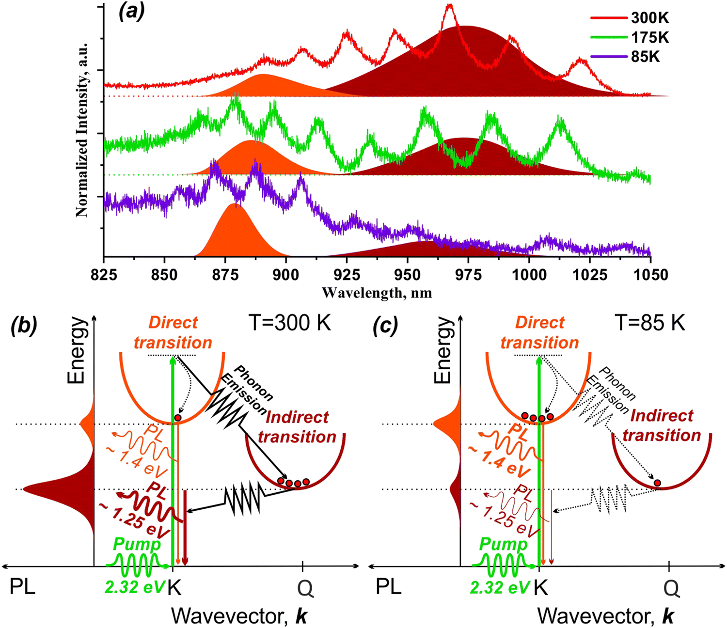 | ||
| Fig. 5 (a) Temperature dependence of photoluminescence. (b and c) Scheme of optical transitions at 300 K and 85 K, respectively. Orange and red contours are simple guides to the eye for direct and indirect transitions, respectively. Conventional fitting by Gaussian or Lorentzian curves is hampered due to the fact that the PL spectra modified by WGM resonance, and the PL of the thick flake are very weak. | ||
As you can see from Fig. 5a, with the decreasing temperature, the broad spectrum at 300 K (see red line) splits into two components at 175 K (see green line), and finally, at 85 K (see violet line), the long-wavelength peak quenches, and the short-wavelength one becomes dominant in the spectrum. Based on such behavior of the PL, we can assume that the observed PL consists of two near peaks. The direct transition is about 1.4 eV, and the indirect transition is about 1.25 eV. The energy of excitation is much higher than both of these (i.e., excitation is non-resonant). Therefore, at room temperature, most of the excited electrons experience phonon-assisted relaxation to the lowest energy state. There, the electrons commit radiative phonon-assisted recombination that provides the peak at 1.25 eV. Although, some electrons relax directly to a higher energy state that has a shorter lifetime (i.e., higher oscillator strength) and recombine directly without a phonon that provides the peak at 1.4 eV. This case is illustrated in Fig. 5b that corresponds to the spectrum at 300 K (see Fig. 5a). With decreasing temperature, the PL peaks become narrow, and the phonons start to freeze out which reduces the effectiveness of the phonon-assisted recombination channel. As a consequence, we can see the separation of direct and indirect peaks and the formation of a “trough” at 930 nm between them (see Fig. 5a, 175 K). At 85 K, the phonons are almost frozen out, and the phonon-assisted channel is ineffective. Therefore, the indirect peak can barely be seen, and the direct channel becomes dominant. This case is illustrated in Fig. 5c that corresponds to the spectrum at 85 K (see Fig. 5a). Although, as discussed earlier, the cavities mainly enhance the tails of the PL peaks. So, the actual energies of transitions are probably slightly higher than those we observe here.
4 Conclusions
To conclude, we investigated the optical properties of nanophotonic WGM disk resonators. The resonators were fabricated from bulk indirect bandgap MoSe2via resistless mechanical scanning probe lithography. The diameter of the cavities varied from 1.4 to 10 μm, and the thickness was 70 nm. A micro-photoluminescence investigation revealed WGM-like PL spectra with various enhancement factors depending on the cavity diameter. It was shown that the optimal cavity diameter is 2.2 μm, which provides an enhancement factor of ≈100 compared to the pristine flake. Scattering experiments and modeling also revealed WGM spectra and confirmed the data obtained by micro-PL. Moreover, we investigated the temperature dependence of a cavity PL. The results showed that the PL has two components – short-wavelength (≈885 nm) and long-wavelength (≈990 nm) components. With decreasing temperature, the long-wavelength component quenches, while the short-wavelength one becomes dominant. Based on these results, we assume that two transitions are simultaneously active in the PL of our structures – direct (≈1.4 eV) and indirect (≈1.25 eV).Thus, in this work, we demonstrated a novel approach to the fabrication of light-emitting nanophotonic devices based on bulk indirect bandgap TMDs and investigated the optical properties of several of them. We believe that this approach might be promising to create other light-emitting nanophotonic devices from bulk TMDs and reveal their fascinating properties.
Author contributions
B. R. B. performed the probe lithography, analyzed the data obtained, and prepared the initial manuscript. F. A. B. fabricated the samples. V. Yu. D., I. A. E., and A. N. S. carried out the micro-photoluminescence investigations. D. A. P. performed a scattering study. S. I. L. and A. A. B. provided theoretical support and calculations. P. A. A. and A. A. B. supervised the research and provided essential contributions to interpreting the results. All coauthors assisted in writing the manuscript.Conflicts of interest
There are no conflicts to declare.Acknowledgements
There is no funding to report. We thank Mikhail M. Glazov and Ivan V. Iorsh for fruitful discussions.References
- K. S. Novoselov, A. K. Geim, S. V. Morozov, D.-e Jiang, Y. Zhang, S. V. Dubonos, I. V. Grigorieva and A. A. Firsov, Science, 2004, 306, 666–669 CrossRef CAS PubMed.
- S. Manzeli, D. Ovchinnikov, D. Pasquier, O. V. Yazyev and A. Kis, Nat. Rev. Mater., 2017, 2, 1–15 Search PubMed.
- D. M. Kennes, M. Claassen, L. Xian, A. Georges, A. J. Millis, J. Hone, C. R. Dean, D. Basov, A. N. Pasupathy and A. Rubio, Nat. Phys., 2021, 17, 155–163 Search PubMed.
- Y. Jing, B. Liu, X. Zhu, F. Ouyang, J. Sun and Y. Zhou, Nanophotonics, 2020, 9, 1675–1694 Search PubMed.
- K. F. Mak and J. Shan, Nat. Photonics, 2016, 10, 216–226 CrossRef CAS.
- M. Bernardi, M. Palummo and J. C. Grossman, Nano Lett., 2013, 13, 3664–3670 CrossRef CAS PubMed.
- M. M. Ugeda, A. J. Bradley, S.-F. Shi, H. Felipe, Y. Zhang, D. Y. Qiu, W. Ruan, S.-K. Mo, Z. Hussain and Z.-X. Shen, et al. , Nat. Mater., 2014, 13, 1091–1095 CrossRef CAS PubMed.
- A. Hanbicki, M. Currie, G. Kioseoglou, A. Friedman and B. Jonker, Solid State Commun., 2015, 203, 16–20 CrossRef CAS.
- P. Tonndorf, R. Schmidt, P. Böttger, X. Zhang, J. Börner, A. Liebig, M. Albrecht, C. Kloc, O. Gordan and D. R. Zahn, et al. , Opt. Express, 2013, 21, 4908–4916 CrossRef CAS PubMed.
- S. Tongay, J. Zhou, C. Ataca, J. Liu, J. S. Kang, T. S. Matthews, L. You, J. Li, J. C. Grossman and J. Wu, Nano Lett., 2013, 13, 2831–2836 CrossRef CAS PubMed.
- F. Benimetskiy, V. Sharov, P. Alekseev, V. Kravtsov, K. Agapev, I. Sinev, I. Mukhin, A. Catanzaro, R. Polozkov and E. Alexeev, et al. , APL Mater., 2019, 7, 101126 CrossRef.
- A. K. Geim and I. V. Grigorieva, Nature, 2013, 499, 419–425 CrossRef CAS PubMed.
- S. Fan, Q. A. Vu, M. D. Tran, S. Adhikari and Y. H. Lee, 2D Mater., 2020, 7, 022005 CrossRef CAS.
- J. Michl, S. Tarasenko, F. Lohof, G. Gies, M. von Helversen, R. Sailus, S. Tongay, T. Taniguchi, K. Watanabe and T. Heindel, et al. , Phys. Rev. B, 2022, 105, L241406 CrossRef CAS.
- K. Tran, J. Choi and A. Singh, 2D Mater., 2020, 8, 022002 CrossRef.
- S. Shabani, D. Halbertal, W. Wu, M. Chen, S. Liu, J. Hone, W. Yao, D. N. Basov, X. Zhu and A. N. Pasupathy, Nat. Phys., 2021, 17, 720–725 Search PubMed.
- A. Goldberg, A. Beal, F. Levy and E. Davis, Philos. Mag., 1975, 32, 367–378 CrossRef CAS.
- A. Beal and H. Hughes, J. Phys. C-Solid State Phys., 1979, 12, 881 CrossRef CAS.
- J. A. Wilson and A. Yoffe, Adv. Phys., 1969, 18, 193–335 CrossRef CAS.
- A. Anedda and E. Fortin, J. Phys. Chem. Solids, 1980, 41, 865–869 CrossRef CAS.
- G. Ermolaev, D. Grudinin, Y. Stebunov, K. V. Voronin, V. Kravets, J. Duan, A. Mazitov, G. Tselikov, A. Bylinkin and D. Yakubovsky, et al. , Nat. Commun., 2021, 12, 1–8 CrossRef PubMed.
- N. Berahim, I. S. Amiri, T. Anwar, S. R. Azzuhri, M. M. Nasir, R. Zakaria, W. Y. Chong, C. K. Lai, S. H. Lee and H. Ahmad, et al. , Results Phys., 2019, 12, 7–11 CrossRef.
- R. Verre, D. G. Baranov, B. Munkhbat, J. Cuadra, M. Käll and T. Shegai, Nat. Nanotechnol., 2019, 14, 679–683 CrossRef CAS PubMed.
- H. Zhang, B. Abhiraman, Q. Zhang, J. Miao, K. Jo, S. Roccasecca, M. W. Knight, A. R. Davoyan and D. Jariwala, Nat. Commun., 2020, 11, 1–9 CrossRef PubMed.
- F. Hu, Y. Luan, M. Scott, J. Yan, D. Mandrus, X. Xu and Z. Fei, Nat. Photonics, 2017, 11, 356–360 CrossRef CAS.
- S. Busschaert, R. Reimann, M. Cavigelli, R. Khelifa, A. Jain and L. Novotny, ACS Photonics, 2020, 7, 2482–2488 CrossRef CAS.
- Y. Ye, Z. J. Wong, X. Lu, X. Ni, H. Zhu, X. Chen, Y. Wang and X. Zhang, Nat. Photonics, 2015, 9, 733–737 CrossRef CAS.
- Y. Li, J. Zhang, D. Huang, H. Sun, F. Fan, J. Feng, Z. Wang and C.-Z. Ning, Nat. Nanotechnol., 2017, 12, 987–992 CrossRef CAS PubMed.
- Z. Fei, M. Scott, D. Gosztola, J. Foley IV, J. Yan, D. Mandrus, H. Wen, P. Zhou, D. Zhang and Y. Sun, et al. , Phys. Rev. B, 2016, 94, 081402 CrossRef.
- B. Munkhbat, B. Küçüköz, D. G. Baranov, T. J. Antosiewicz and T. O. Shegai, Laser Photonics Rev., 2022, 17, 2200057 CrossRef.
- A. R. Khan, L. Zhang, K. Ishfaq, A. Ikram, T. Yildrim, B. Liu, S. Rahman and Y. Lu, Adv. Funct. Mater., 2022, 32, 2105259 CrossRef CAS.
- A. Autere, H. Jussila, Y. Dai, Y. Wang, H. Lipsanen and Z. Sun, Adv. Mater., 2018, 30, 1705963 CrossRef PubMed.
- N. Muhammad, Y. Chen, C.-W. Qiu and G. P. Wang, Nano Lett., 2021, 21, 967–972 CrossRef CAS PubMed.
- N. Bernhardt, K. Koshelev, S. J. White, K. W. C. Meng, J. E. Froch, S. Kim, T. T. Tran, D.-Y. Choi, Y. Kivshar and A. S. Solntsev, Nano Lett., 2020, 20, 5309–5314 CrossRef CAS PubMed.
- S. Tongay, J. Zhou, C. Ataca, K. Lo, T. S. Matthews, J. Li, J. C. Grossman and J. Wu, Nano Lett., 2012, 12, 5576–5580 CrossRef CAS PubMed.
- L. Wang, X. Zhou, S. Yang, G. Huang and Y. Mei, Photon. Res., 2019, 7, 905–916 CrossRef CAS.
- A. Krasnok, S. Lepeshov and A. Alú, Opt. Express, 2018, 26, 15972–15994 CrossRef CAS PubMed.
- T. Ren, P. Song, J. Chen and K. P. Loh, ACS Photonics, 2018, 5, 353–358 CrossRef CAS.
- E. M. Purcell, Confined Electrons and Photons, Springer, 1995, pp. 839–839 Search PubMed.
- L. Eswaramoorthy, S. Mokkapati and A. Kumar, J. Phys. D: Appl. Phys., 2022, 55, 225103 CrossRef.
- H. Ling, R. Li and A. R. Davoyan, ACS Photonics, 2021, 8, 721–730 CrossRef CAS.
- C.-H. Cho, C. O. Aspetti, J. Park and R. Agarwal, Nat. Photonics, 2013, 7, 285–289 CrossRef CAS PubMed.
- M. Fujita, Nat. Photonics, 2013, 7, 264–265 CrossRef CAS.
- J. Valenta, M. Greben, S. Dyakov, N. Gippius, D. Hiller, S. Gutsch and M. Zacharias, Sci. Rep., 2019, 9, 1–9 CrossRef CAS PubMed.
- Y. Gong, S. Ishikawa, S.-L. Cheng, M. Gunji, Y. Nishi and J. Vǔković, Phys. Rev. B: Condens. Matter Mater. Phys., 2010, 81, 235317 CrossRef.
- R. D. Kekatpure and M. L. Brongersma, Nano Lett., 2008, 8, 3787–3793 CrossRef CAS PubMed.
- P. M. Fauchet, J. Lumin., 1998, 80, 53–64 CrossRef CAS.
- R. Elliman, M. Forcales, A. Wilkinson and N. Smith, Nucl. Instrum. Methods Phys. Res., Sect. B, 2007, 257, 11–14 CrossRef CAS.
- B. K. Ridley, Quantum processes in semiconductors, Oxford university press, 2013 Search PubMed.
- C. Hsu, R. Frisenda, R. Schmidt, A. Arora, S. M. de Vasconcellos, R. Bratschitsch, H. S. van der Zant and A. Castellanos-Gomez, Adv. Opt. Mater., 2019, 7, 1900239 CrossRef.
- G.-H. Jung, S. Yoo and Q.-H. Park, Nanophotonics, 2019, 8, 263–270 Search PubMed.
- J. Sung, D. Shin, H. Cho, S. W. Lee, S. Park, Y. D. Kim, J. S. Moon, J.-H. Kim and S.-H. Gong, Nat. Photonics, 2022, 16, 792–797 CrossRef CAS.
- X. Du, I. Skachko, A. Barker and E. Y. Andrei, Nat. Nanotechnol., 2008, 3, 491–495 CrossRef CAS PubMed.
- J. J. Schwartz, H.-J. Chuang, M. R. Rosenberger, S. V. Sivaram, K. M. McCreary, B. T. Jonker and A. Centrone, ACS Appl. Mater. Interfaces, 2019, 11, 25578–25585 CrossRef CAS PubMed.
- R. Garcia, A. W. Knoll and E. Riedo, Nat. Nanotechnol., 2014, 9, 577–587 CrossRef CAS PubMed.
- B. Borodin, F. Benimetskiy, V. Y. Davydov, I. Eliseyev, S. Lepeshov, A. Bogdanov and P. Alekseev, J. Phys.: Conf. Ser., 2021, 012020 CrossRef CAS.
- B. Borodin, F. Benimetskiy and P. Alekseev, J. Phys.: Conf. Ser., 2021, 012090 CrossRef.
- C. Schinke, P. Christian Peest, J. Schmidt, R. Brendel, K. Bothe, M. R. Vogt, I. Kröger, S. Winter, A. Schirmacher and S. Lim, et al. , AIP Adv., 2015, 5, 067168 CrossRef.
- P. B. Johnson and R.-W. Christy, Phys. Rev. B: Solid State, 1972, 6, 4370 CrossRef CAS.
- V. Ardizzone, L. De Marco, M. De Giorgi, L. Dominici, D. Ballarini and D. Sanvitto, Nanophotonics, 2019, 8, 1547–1558 CAS.
- M. Li, I. Sinev, F. Benimetskiy, T. Ivanova, E. Khestanova, S. Kiriushechkina, A. Vakulenko, S. Guddala, M. Skolnick and V. M. Menon, et al. , Nat. Commun., 2021, 12, 1–10 CrossRef PubMed.
- I. Sinev, M. Li, F. Benimetskiy, T. Ivanova, S. Kiriushechkina, A. Vakulenko, S. Guddala, D. Krizhanovskii, A. Samusev and A. Khanikaev, J. Phys.: Conf. Ser., 2021, 012142 CrossRef CAS.
- N. Dong, Y. Li, Y. Feng, S. Zhang, X. Zhang, C. Chang, J. Fan, L. Zhang and J. Wang, Sci. Rep., 2015, 5, 1–10 Search PubMed.
- F. Ceccarelli, G. Acconcia, A. Gulinatti, M. Ghioni, I. Rech and R. Osellame, Adv. Quantum Technol., 2021, 4, 2000102 CrossRef CAS.
- S. A. Dyakov, M. V. Stepikhova, A. A. Bogdanov, A. V. Novikov, D. V. Yurasov, M. V. Shaleev, Z. F. Krasilnik, S. G. Tikhodeev and N. A. Gippius, Laser Photonics Rev., 2021, 15, 2000242 CrossRef CAS.
- T. V. Shubina, M. Remškar, V. Y. Davydov, K. G. Belyaev, A. A. Toropov and B. Gil, Ann. Phys., 2019, 531, 1800415 CrossRef.
- E. Malic, M. Selig, M. Feierabend, S. Brem, D. Christiansen, F. Wendler, A. Knorr and G. Berghäuser, Phys. Rev. Mater., 2018, 2, 014002 CrossRef CAS.
- O. Smirnova, I. Eliseyev, A. Rodina and T. Shubina, J. Phys.: Conf. Ser., 2020, 012038 CrossRef CAS.
- S. Brem, A. Ekman, D. Christiansen, F. Katsch, M. Selig, C. Robert, X. Marie, B. Urbaszek, A. Knorr and E. Malic, Nano Lett., 2020, 20, 2849–2856 CrossRef CAS PubMed.
Footnote |
| † Electronic supplementary information (ESI) available. See DOI: https://doi.org/10.1039/d2nh00465h |
| This journal is © The Royal Society of Chemistry 2023 |