
Abnormal behavior of preferred formation of the cationic vacancies from the interior in a γ-GeSe monolayer with the stereo-chemical antibonding lone-pair state†
Changmeng
Huan
 ab,
Yongqing
Cai
*c,
Devesh R.
Kripalani
d,
Kun
Zhou
d and
Qingqing
Ke
*ab
ab,
Yongqing
Cai
*c,
Devesh R.
Kripalani
d,
Kun
Zhou
d and
Qingqing
Ke
*ab
aSchool of Microelectronics Science and Technology, Sun Yat-sen university, Zhuhai 519082, China. E-mail: keqingq@mail.sysu.edu.cn
bGuangdong Provincial Key Laboratory of Optoelectronic Information Processing Chips and Systems, Sun Yat-sen University, Zhuhai 519082, China
cJoint Key Laboratory of the Ministry of Education, Institute of Applied Physics and Materials Engineering, University of Macau, Taipa, Macau, China. E-mail: yongqingcai@um.edu.mo
dSchool of Mechanical and Aerospace Engineering, Nanyang Technological University, 50 Nanyang Avenue, Singapore 639798, Singapore
First published on 24th January 2023
Abstract
Two-dimensional (2D) materials tend to have the preferable formation of vacancies at the outer surface. Here, contrary to the normal notion, we reveal a type of vacancy that thermodynamically initiates from the interior part of the 2D backbone of germanium selenide (γ-GeSe). Interestingly, the Ge-vacancy (VGe) in the interior part of γ-GeSe possesses the lowest formation energy amongst the various types of defects considered. We also find a low diffusion barrier (1.04 eV) of VGe, which is half of those of sulfur vacancies in MoS2. The facile formation of mobile VGe is rooted in the antibonding coupling of the lone-pair Ge 4s and Se 4p states near the valence band maximum, which also exists in other gamma-phase MX (M = Sn, Ge; X = S, Te). The VGe is accompanied by a shallow acceptor level in the band gap and induces strong infrared light absorption and p-type conductivity. The VGe located in the middle cationic Ge sublattice is well protected by the surface Se layers – a feature that is absent in other atomically thin materials. Our work suggests that the unique well-buried inner VGe, with the potential of forming structurally protected ultrathin conducting filaments, may render the GeSe layer an ideal platform for quantum emitting, memristive, and neuromorphic applications.
New conceptsSeeking stable and benign atomic vacancies in materials is critical for constructing the latest state-of-the-art neuromorphic devices and forming ionic conducting channels in solid ionic conductors. For instance, vacancy defects at grain boundaries account for the resistive switching in MoS2 vacancies. While the vacancy in phosphorene is highly mobile, its strong reaction with oxygen and poor conductivity limit its applications. Identifying materials with highly mobile and controllable vacancies is critical for artificial synapse and neuromorphic electronics. However, no 2D materials have been found to have a naturally inner-born vacancy with mobile activity. Contrary to the normal notion, here we reveal an abnormal behavior that the vacancy preferably initiates from the interior part of the 2D backbone in γ-GeSe, a novel hexagonal phase of GeSe synthesized recently. This is in stark contrast to vacancies in transition metal dichalcogenides, which have predominantly anionic vacancies formed at the outer surface. The facile formation of Ge vacancies in γ-GeSe is rooted in the antibonding coupling of the lone-pair Ge 4s and Se 4p states. Importantly, the diffusion barrier of the Ge vacancy is only half that of the S vacancy in the famous MoS2, making γ-GeSe highly appealing for neuromorphic switching. |
Introduction
Group IV monochalcogenides MX (M = Ge, Sn, Pb; X = S, Se, Te) are a family of emerging 2D layered materials which are gaining extensive interest in thermoelectric,1,2 photocatalysis,3,4 and ferroelectric5,6 fields. Among the various MXs, GeSe deserves particular attention, owing to recent papers reporting on its outstanding photovoltaic efficiency,7 excellent optoelectronic properties,8 and electric-field induced room temperature antiferroelectric–ferroelectric phase transition,9 as well as its inherent chemical stability and environmental sustainability.Thus far, most of the studies on MX are all based on the well-studied orthorhombic phase (α-phase) with a black-phosphorus-like structure. Recently, a hexagonal phase of GeSe (γ-phase) with two merged blue-phosphorus-like layers has been synthesized on a h-BN substrate by chemical vapor deposition (CVD), showing an intriguing electronic conductivity that is even higher than that of graphite.10 Unlike theoretical predictions, the deposited γ-GeSe shows an A–B′ stacked non-centrosymmetric atomic structure.11 This new structure has aroused great interest with respect to the strain-tunable electronic structure and spontaneous polarization,12,13 van der Waals heterostructures,14 and fast Li-ion intercalation properties15 through first-principles calculations.
Point defects are inevitably introduced during the preparation process and have significant effects on the electronic, optical, and magnetic properties of 2D materials.16–19 For instance, oxygen vacancies in ultrathin WO3 layers can introduce an intermediate band and induce strong infrared light absorption, enabling IR-driven CO2 splitting into CO and O2.18 Cr or I atom vacancies can induce a ferromagnetic to antiferromagnetic transition in CrI3.19 Therefore, it is of crucial importance to understand the nature of intrinsic defects and their impact on the properties of γ-GeSe.
In this work, using first-principles calculations, we discovered an abnormal type of defect that is likely to exist in this new phase of GeSe. Through investigating the intrinsic point defects in the hexagonal phase γ-GeSe monolayer, including vacancies, anti-site defects, and interstitials, an energetically favorable formation of the Ge vacancy located at the interior region is predicted, which is distinctive from the overwhelming dominance of anionic vacancies at the surface in existing 2D compounds. The advantage of the spontaneous formation of such inner vacancy voids is apparent as it allows the manipulation of robust and structurally intact ordering of the vacancy for quantum emission or resistive switching. Thus far, achieving similar functionality in other 2D materials has to resort to generating surface defects such as halogen vacancies in transition metal dichalcogenides, which tend to be subjected to structural poisoning and environmental disturbance.20 Through further analysis of its orbital hybridization diagram, we attribute the formation of this facile defect to the significant population of lone-pair Ge 4s and Se 4p states near the valence band maximum, which also exists in other gamma-phase MX (M = Sn, Ge; X = S, Te).
Results and discussion
Structures and stability of perfect γ-GeSe
Monolayer γ-GeSe is a four-atom-thick (Se–Ge–Ge–Se sequence, Fig. 1a) monolayer with a buckled honeycomb lattice structure that can be exfoliated from its bulk phase (space group P63mc, Fig. 1b).10 The lattice dynamic stability of monolayer γ-GeSe is confirmed by the lack of imaginary phonon modes in the phonon dispersion spectra, as shown in Fig. 1c. Furthermore, its thermodynamic stability is also validated through AIMD calculation (Fig. 1d), where the total energy undergoes a small fluctuation, and the structural snapshot at 10 ps shows that the atoms are only slightly displaced near their equilibrium positions with no structural corruption, thus confirming the excellent thermostability of this phase.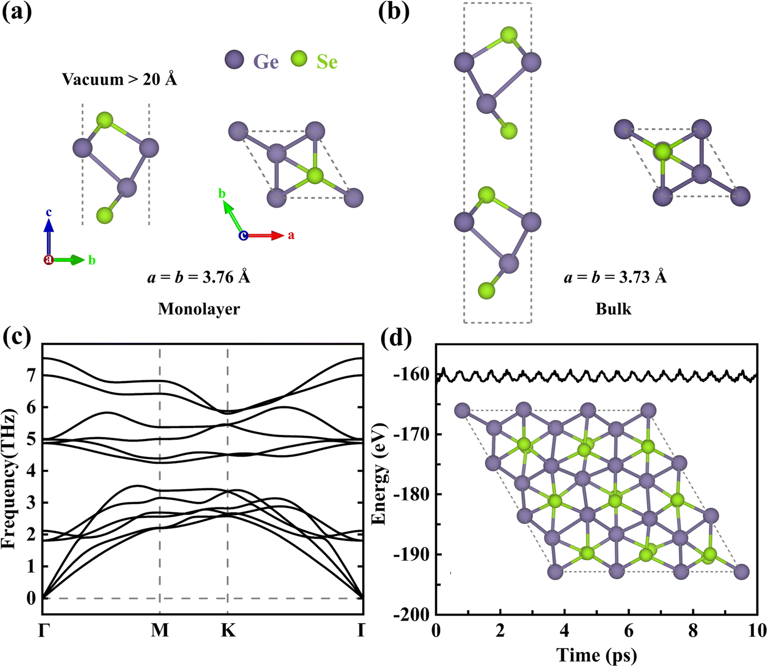 | ||
| Fig. 1 Front and top views of the unit cell of (a) monolayer and (b) bulk γ-GeSe, (c) phonon spectra of monolayer γ-GeSe, and (d) evolution of the total energy from AIMD calculation at 300 K and a snapshot of the monolayer supercell at 10 ps. | ||
Formation of defects in monolayer γ-GeSe
The point defects in monolayer γ-GeSe were cataloged into three types: (I) vacancies: a single Ge atom vacancy (VGe), a single Se atom vacancy (VSe), a double Ge atom vacancy (V2Ge), a double Se atom vacancy (V2Se), and a Ge–Se vacancy (VGe–Se); (II) anti-site defects: where a Ge atom substitutes an Se atom (GeSe) or an Se atom substitutes a Ge atom (SeGe); (III) interstitials: an interstitial Ge atom (IGe) and an interstitial Se atom (ISe). The double vacancies (V2Se, VGe–Se, V2Ge) are generated by removing the nearest-neighboring atoms without considering any asymmetry in this work. The optimized geometries of defective γ-GeSe monolayers in the neutral charge state are presented in Fig. S1 (ESI†). It is found that all defective supercells show slight structural changes relative to the perfect one, while single-point defects exhibit relatively localized distortions relative to double-point defects.The structural stability and thermodynamics of the different point defects can be evaluated from their formation energy (Ef), which can be defined as21
| Ef = Ed − Ep − ∑niμi | (1) |
| μGeSe − μOSe < μGe < μOGe | (2) |
The Ef values of all the investigated defects in monolayer γ-GeSe as a function of μGe are plotted in Fig. 2, and the Ef of such defects in monolayer α-GeSe (Fig. S2, ESI†) are also calculated for comparison. Surprisingly, the VGe defect shows the lowest Ef over the whole range of Ge chemical potential values despite its formation requiring the breaking of six covalent bonds and the removal of cationic Ge from the inner layers of γ-GeSe. This preferred formation of cationic vacancies is quite different from the case of MoX2 (X = S, Se, Te), where X vacancies in the outer layer are easier to form.23–25 Furthermore, the formation energy of VGe (0.92/0.46 eV) in γ-GeSe is even lower than that in the common α-GeSe phase (1.16/0.84 eV), where Ge atoms are located in the outer layer and lie exposed on the surface. The effect of concentration on the energetics of the vacancy is considered by comparing the Ef of the single vacancy in 2 × 2, 3 × 3 and 4 × 4 supercells, and the Ef of the single vacancy and double vacancies in a 3 × 3 supercell, respectively. The results in Fig. S3 (ESI†) indicate that this abnormal behavior of preferred formation of cationic vacancies from the interior exists in all conditions considered, and the lower the vacancy concentration, the lower the Ef of VGe. In addition, as shown in Fig. S4 (ESI†), the interaction energies (Eint)26 of di-vacancies is smaller than that of two separated mono-vacancies, indicating that the separated mono-vacancies in monolayer γ-GeSe tend to combine into vacancy pairs. This is consistent with the scenario in graphene but in contrast to that in MoS2, where separated mono-vacancies are more energetically favored.25,27 On the other hand, AIMD simulation has validated the thermodynamic stability of the γ-GeSe supercell containing different defects (Fig. S5, ESI†). Therefore, Ge vacancies and their clusters are the most likely defect in monolayer γ-GeSe. Certainly, other defects can also be achieved by irradiation and ion implantation, which are widely accepted approaches for the introduction and control of defects.
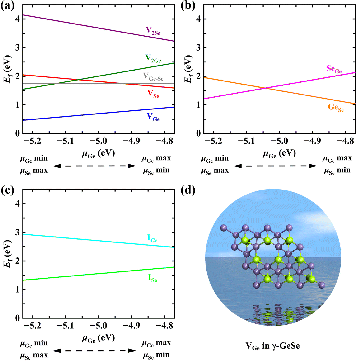 | ||
| Fig. 2 Formation energies of monolayer γ-GeSe containing (a) vacancy, (b) anti-site, and (c) interstitial defects as functions of μGe in the range from −5.23 eV (Ge-poor) to −4.77 eV (Ge-rich). (d) Top view of the most stable defect (VGe) in the γ-GeSe monolayer, where γ-GeSe can remain stable with respect to the formation of bulk Ge (μGe = −4.77 eV) or the Se6 molecular crystal (μGe = −5.23 eV). | ||
Mechanism of thermodynamically preferred Ge vacancy formation in the inner layer
According to the revised lone pair model,28 the asymmetrically layered crystal structure is attributed to the stereo-chemically active lone pairs, where the filled s2 electrons in the lower oxidation state of the cation show stereochemical activity that arises from the cation s–anion p coupling (anti-bonding states). The distorted crystal structure is dependent on the strength of the interaction between the cation s states and the anion p states, that is, on their relative energies. Therefore, the relatively low-symmetry crystal structures of γ-GeSe (P63mc) arise from the Ge 4s–Se 4p coupling, which is in contrast to the high-symmetry rocksalt structure (Fm![[3 with combining macron]](https://www.rsc.org/images/entities/char_0033_0304.gif) m) of PbSe and PbS, where the energy of the Pb 6s electrons is so far away from the energies of Se 4p and S 3p electrons that the 6s2 electrons are certainly stereo-chemically inert.
m) of PbSe and PbS, where the energy of the Pb 6s electrons is so far away from the energies of Se 4p and S 3p electrons that the 6s2 electrons are certainly stereo-chemically inert.
The lone-pair state of Ge in γ-GeSe can be visualized from the isosurface plots of the electron localization function (ELF), as shown in Fig. 3a and b. The projected density of states (PDOS) in Fig. 3c confirms the orbital hybridization of Ge 4s, Ge 4p, and Se 4p states in the blue-shaded regions, where the little Ge 4p shows a net stabilizing effect and is essential for Ge on-site hybridization while the Ge 4s lone-pairs contribute significantly at the anti-bonding level. In addition, there is also a strong Ge 4s state component in the bottom-most conduction band of γ-GeSe, which may be responsible for the localized electrons around Se atoms, as observed in the ELF plot (Fig. 3a). The strong Ge 4s–Se 4p antibonding coupling near the VBM of γ-GeSe is also reflected from the analysis of k-dependent crystal orbital Hamilton populations (COHPs) based on the LOBSTER code in the PBE method.29–32 In Fig. 3d, the positive/negative values in COHPs represent the antibonding/bonding state and the magnitude indicates the strength of orbital coupling.
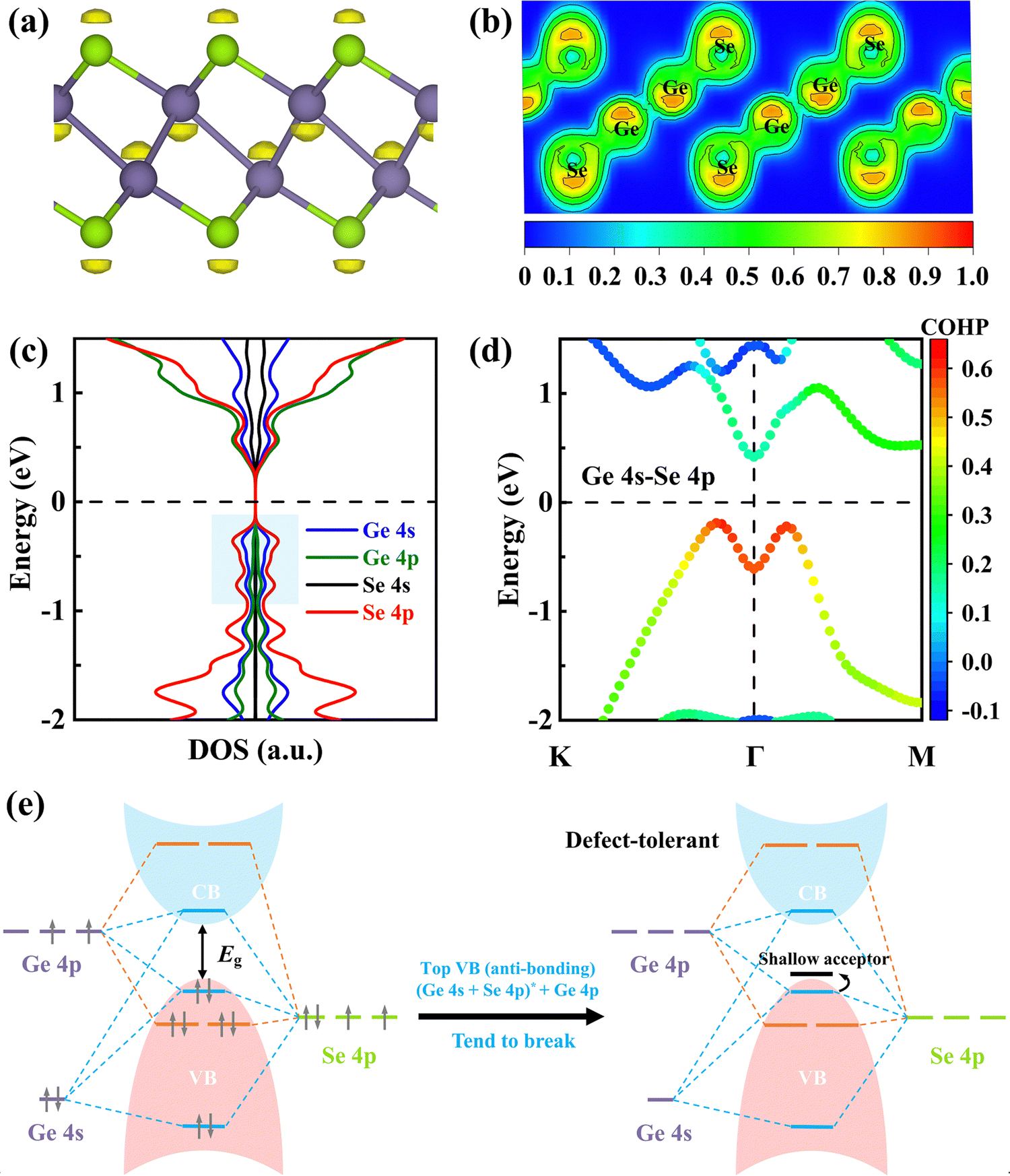 | ||
| Fig. 3 (a) ELF of the γ-GeSe monolayer supercell (isosurface level: 0.813), showing the lone pairs in yellow. (b) 2D ELF contour map of the (110) plane in γ-GeSe. (c) PDOS of γ-GeSe using the PBE functional. (d) The k-dependent COHPs of Ge 4s–Se 4p orbitals of the γ-GeSe monolayer. (e) Schematic energy level diagram of the interactions in γ-GeSe and the tendency of forming a Ge vacancy and its associated shallow acceptor level. The Fermi level is set to 0. | ||
Based on the above results, we summarized the schematic energy level diagram of the interactions in γ-GeSe in Fig. 3e. The occupied anti-bonding state consisting of Ge 4s and Se 4p coupling does not gain electronic energy, thus tending to break the Ge–Se bond and form a Ge vacancy. This mechanism is akin to the s–p antibonding coupling in CH3NH3PbI3 and p–d antibonding coupling in CuInSe2.33,34 The electronic structure of γ-GeSe resembles a defect-tolerant electronic structure known to lead to shallow defects.35
Using first-principles calculations, Luo et al.11 demonstrated that the gamma-phase of group-IV monochalcogenides (γ-MX, M = Ge, Sn; X = S, Te) can be stabilized in the monolayer limit. Therefore, we conducted a calculation to explore whether the abnormal behavior of cationic vacancies also exists in these γ-MXs with the same symmetric structure. The Ef of the vacancies is calculated using the same method as for γ-GeSe and the results are plotted in Fig. 4. It is found that the preferred formation of inner cationic vacancies is not unique to γ-GeSe, but also applicable to these γ-MXs. The k-dependent COHPs show that there is M 4s–X 4p antibonding coupling near the VBM of all these γ-MXs. In addition, this abnormal behavior in these γ-MXs is positively related to the strength of anti-bonding states. The Ef of the cationic vacancy in GeS and SnS with strong anti-bonding states is significantly lower than that of GeTe and SnTe with weak anti-bonding states. And the energy difference (Ef_mim) between the minimum Ef of cationic and anionic vacancies decreases with the weakening of the anti-bonding state. The above results indicate that the presence of the antibonding lone-pair state indeed accounts for the abnormal behavior of preferred formation of cationic vacancies from the interior, especially in γ-MX (M = Sn, Ge; X = S, Se, Te).
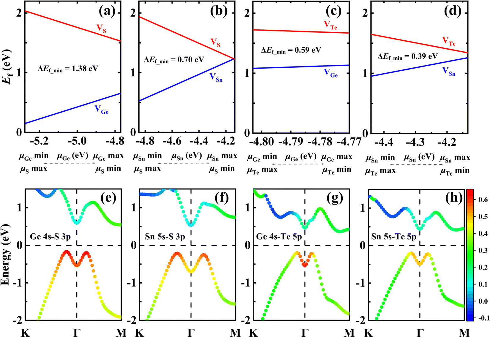 | ||
| Fig. 4 Formation energies of monolayer γ-GeS (a), γ-SnS (b), γ-GeTe (c), and γ-SnTe (d) containing vacancies as functions of μcation. The k-dependent COHPs of cation 4s–anion 4p orbitals of monolayer γ-GeS (e), γ-SnS (f), γ-GeTe (g), and γ-SnTe (h) using the PBE functional. | ||
Effects of VGe on the electronic properties and light absorption
The diffusion energy barrier (Eb) and pathway to the neighboring site of VGe are plotted in Fig. 5a. The Eb of VGe (1.04 eV) is much larger than that of the phosphorus vacancy in phosphorene (0.30 eV) but lower than that of the sulfur vacancy (2.27 eV) in MoS2, indicating that it has moderate activity that can facilitate experimental observation.36 To figure out the effect of VGe on the electronic properties, we analyzed the ELF results, unfolded band structures, and local density of states (LDOS) for VGe-GeSe as well as for the perfect γ-GeSe. The ELF results in Fig. 5b show that the Ge and Se atoms around the VGe give rise to distinct localized electrons relative to the perfect supercell (Fig. S6a–c, ESI†), which may alter their interaction with gas molecules for gas sensing. As shown in Fig. S6d (ESI†), the perfect γ-GeSe monolayer is a semiconductor with an indirect bandgap of 0.99 eV in the HSE06 hybrid functional. However, the presence of VGe in γ-GeSe (Fig. 5c) pushes upwardly the topmost valence band with its energy exceeding the Fermi level (EF) and forming a shallow acceptor level, resulting in an insulator-to-metal transition and p-type nature. The LDOS of VGe-GeSe indicates that the defect state is composed of the contributions from both the Ge and Se atoms. The above results prove that the nature of the shallow acceptor level of VGe is attributed to the special antibonding character (s–p coupling) at the top valence bands, which pushes the topmost valence band upwards to form a shallow acceptor level.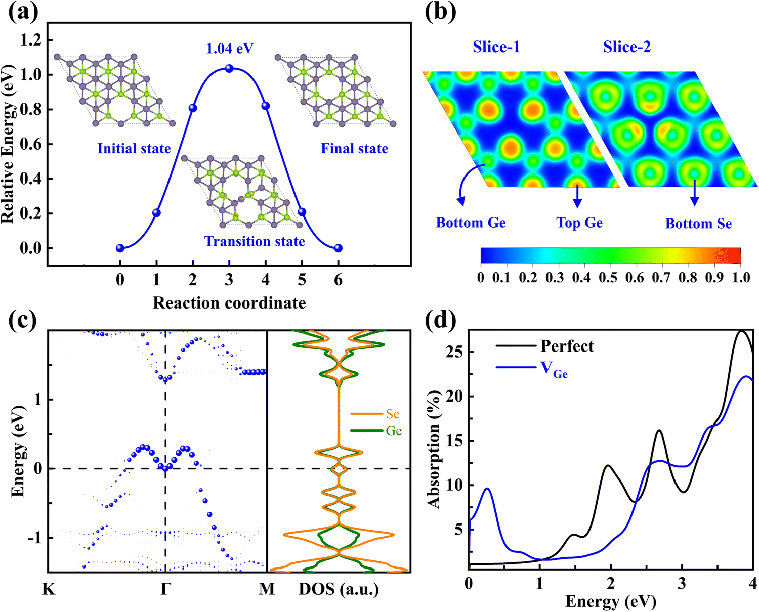 | ||
| Fig. 5 (a) Configurations and diffusion barrier of VGe, (b) 2D ELF contour maps of the (001) plane, (c) unfolded band structure and LDOS of monolayer VGe-GeSe, and (d) absorption spectra of monolayer γ-GeSe with and without VGe. The Fermi level is set to 0. | ||
Since changes in the electronic structures can have a significant impact on the optical properties, the light absorption of γ-GeSe monolayers with and without VGe are calculated, and the results are plotted in Fig. 5d. The perfect γ-GeSe monolayer exhibits strong absorption in the range from ultraviolet to visible light, while the presence of VGe results in a significant change in the absorption spectrum, where it shows a strong peak in the infrared range due to the shallow intermediate gap state extending to the edge of the topmost valence band. In addition, due to the weak Coulomb screening effect in layered materials37,38 and considering the superb light utilization at the near-infrared region of its cousin phases,39 it is highly appealing to explore the excitonic behavior of this new hexagonal polymorph of GeSe in the future.
Conclusions
In summary, we reveal the abnormal behavior of atomic defects in the recently synthesized new hexagonal phase of GeSe, as well as theoretically predicted hexagonal phase MX (M = Sn, Ge; X = S, Te). Different from the common fact that atomic defects, especially vacancies, are predominantly found at the surface due to the lower atomic coordination number, here, we demonstrate that γ-GeSe is a unique system showing the abnormal preference of forming Ge vacancies in the central region. This is in stark contrast to the formation of surface defects in common 2D compounds such as transition metal dichalcogenides, which are predominantly anionic vacancies. Our analysis of the orbital hybridization diagram suggests that the strong Ge 4s–Se 4p antibonding coupling near the VBM of γ-GeSe largely accounts for the tendency of breaking the Ge–Se bond, and accordingly, the relatively facile removal of Ge. The subsurface Ge vacancy located in the middle cationic Ge sublattice, accompanied by a shallow acceptor defect level, is well protected by the surface Se layers – a feature that is absent in other atomically thin materials. This renders the formation of sealed voids inside the layer which may be harnessed for quantum emitters and sensors, as well as for conducting filaments in neuromorphic applications with the agglomeration of Ge vacancy clusters.Methods
First-principles calculations were carried out by the Vienna ab initio simulation package (VASP) with the projector augmented wave (PAW) method.40,41 The generalized gradient approximation (GGA) with the Perdew–Burke–Ernzerhof (PBE) functional was employed to describe the exchange–correlation energy.42 The defective γ-GeSe monolayers were constructed based on a 3 × 3 × 1 supercell with a vacuum layer thickness larger than 20 Å. The energy cutoff and gamma centered k-meshes were set to be 400 eV and 5 × 5 × 1 for structural optimization, respectively. The convergence threshold for the residual force and total energy were 0.005 eV Å−1 and 10−6 eV, respectively. The DFT-D3 method was employed to describe the weak van der Waals interaction.43,44 The Heyd–Scuseria–Ernzerhof (HSE06) hybrid functional45 and VASPKIT code46 were used to evaluate the unfolded electronic structures of the supercell. Thermal and dynamic stability were verified by ab initio molecular dynamics (AIMD)47 simulations at 300 K with a time step of 2 fs and phonon dispersion calculations based on the PHONOPY code,48 respectively. To evaluate the diffusion energy barriers of defects, the climbing-image nudged elastic band (CI-NEB) method was performed.49Author contributions
Huan CM performed the calculations and wrote the original draft. Kripalani DR and Zhou K assisted in the analysis and drafted the manuscript. Cai YQ and Ke QQ guided the idea and finalized the manuscript. All authors participated in general discussion and the manuscript revision.Conflicts of interest
The authors declare that they have no conflict of interest.Acknowledgements
This work was supported by the 100 Talents Program of Sun Yat-sen University (Grant 76220-18841201), the National Natural Science Foundation of China (Grant 22022309), the GuangDong Basic and Applied Basic Research Foundation (2021B1515120025) and the Natural Science Foundation of Guangdong Province, China (2021A1515010024), the University of Macau (SRG2019-00179-IAPME, MYRG2020-00075-IAPME) and the Science and Technology Development Fund from Macau SAR (FDCT-0163/2019/A3).References
- Y. Yu, X. Xu, Y. Wang, B. H. Jia, S. Huang, X. B. Qiang, B. Zhu, P. J. Lin, B. B. Jiang, S. X. Liu, X. Qi, K. F. Pan, D. Wu, H. Z. Lu, M. Bosman, S. J. Pennycook, L. Xie and J. Q. He, Nat. Commun., 2022, 13, 5612 CrossRef CAS PubMed.
- H. Jang, J. H. Park, H. S. Lee, B. Ryu, S. D. Park, H. A. Ju, S. H. Yang, Y. M. Kim, W. H. Nam, H. Wang, J. Male, G. J. Snyder, M. Kim, Y. S. Jung and M. W. Oh, Adv. Sci., 2021, 8, 2100895 CrossRef CAS PubMed.
- Z. Shu and Y. Q. Cai, J. Mater. Chem. A, 2021, 9, 16056–16064 RSC.
- S. Li, Z. C. Zhao, J. B. Li, H. Liu, M. S. Liu, Y. Q. Zhang, L. Z. Su, A. I. Perez-Jimenez, Y. C. Guo, F. Yang, Y. Liu, J. Z. Zhao, J. M. Zhang, L. D. Zhao and Y. H. Lin, Small, 2022, 18, 2202507 CrossRef CAS PubMed.
- O. J. Clark, I. Wadgaonkar, F. Freyse, G. Springholz, M. Battiato and J. Sanchez-Barriga, Adv. Mater., 2022, 34, 2200323 CrossRef CAS PubMed.
- K. Jeong, H. Lee, C. Lee, L. H. Wook, H. Kim, E. Lee and M. H. Cho, Appl. Mater. Today, 2021, 24, 101122 CrossRef.
- S. C. Liu, C. M. Dai, Y. Min, Y. Hou, A. H. Proppe, Y. Zhou, C. Chen, S. Chen, J. Tang, D. J. Xue, E. H. Sargent and J. S. Hu, Nat. Commun., 2021, 12, 670 CrossRef CAS PubMed.
- B. Yan, B. Ning, G. X. Zhang, D. H. Zhou, X. Shi, C. X. Wang and H. Q. Zhao, Adv. Opt. Mater., 2022, 10, 2102413 CrossRef CAS.
- Z. Guan, Y. Zhao, X. Wang, N. Zhong, X. Deng, Y. Zheng, J. Wang, D. Xu, R. Ma, F. Yue, Y. Cheng, R. Huang, P. Xiang, Z. Wei, J. Chu and C. Duan, ACS Nano, 2022, 16, 1308–1317 CrossRef CAS PubMed.
- S. Lee, J. E. Jung, H. G. Kim, Y. Lee, J. M. Park, J. Jang, S. Yoon, A. Ghosh, M. Kim, J. Kim, W. Na, J. Kim, H. J. Choi, H. Cheong and K. Kim, Nano Lett., 2021, 21, 4305–4313 CrossRef CAS PubMed.
- N. Luo, W. Duan, B. I. Yakobson and X. Zou, Adv. Funct. Mater., 2020, 30, 2000533 CrossRef CAS.
- C. M. Huan, P. Wang, B. H. He, Y. Q. Cai and Q. Q. Ke, 2D Mater., 2022, 9, 045014 CrossRef.
- H.-g Kim and H. J. Choi, J. Mater. Chem. C, 2021, 9, 9683–9691 RSC.
- C. M. Huan, P. Wang, B. T. Liu, B. H. He, Y. Q. Cai and Q. Q. Ke, J. Mater. Chem. C, 2022, 10, 10995–11004 RSC.
- Z. Shu, X. Y. Cui, B. W. Wang, H. J. Yan and Y. Q. Cai, ChemSusChem, 2022, 15, 202200564 CrossRef PubMed.
- C. M. Huan, P. Wang, B. H. He, Y. Q. Cai and Q. Q. Ke, J. Mater. Chem. C, 2022, 10, 1839–1849 RSC.
- W. Xu, L. Gan, R. Wang, X. Wu and H. Xu, ACS Appl. Mater. Interfaces, 2020, 12, 19110–19115 CrossRef CAS PubMed.
- L. Liang, X. Li, Y. Sun, Y. Tan, X. Jiao, H. Ju, Z. Qi, J. Zhu and Y. Xie, Joule, 2018, 2, 1004–1016 CrossRef CAS.
- R. Wang, Y. Su, G. Yang, J. Zhang and S. Zhang, Chem. Mater., 2020, 32, 1545–1552 CrossRef CAS.
- V. K. Sangwan, D. Jariwala, I. S. Kim, K. S. Chen, T. J. Marks, L. J. Lauhon and M. C. Hersam, Nat. Nanotechnol., 2015, 10, 403–406 CrossRef CAS PubMed.
- H. F. Chen, H. J. Yan and Y. Q. Cai, Chem. Mater., 2022, 34, 1020–1029 CrossRef CAS.
- A. F. Kohan, G. Ceder, D. Morgan and C. G. V. d Walle, Phys. Rev. B: Condens. Matter Mater. Phys., 2000, 61, 15019 CrossRef CAS.
- D. Edelberg, D. Rhodes, A. Kerelsky, B. Kim, J. Wang, A. Zangiabadi, C. Kim, A. Abhinandan, J. Ardelean, M. Scully, D. Scullion, L. Embon, R. Zu, E. J. G. Santos, L. Balicas, C. Marianetti, K. Barmak, X. Zhu, J. Hone and A. N. Pasupathy, Nano Lett., 2019, 19, 4371–4379 CrossRef CAS PubMed.
- M. B. Kanoun, Surf. Interfaces, 2021, 27, 101442 CrossRef CAS.
- W. Zhou, X. Zou, S. Najmaei, Z. Liu, Y. Shi, J. Kong, J. Lou, P. M. Ajayan, B. I. Yakobson and J. C. Idrobo, Nano Lett., 2013, 13, 2615–2622 CrossRef CAS PubMed.
- D. D. Cuong, B. Lee, K. M. Choi, H. S. Ahn, S. Han and J. Lee, Phys. Rev. Lett., 2007, 98, 129903 CrossRef.
- G. D. Lee, C. Z. Wang, E. Yoon, N. M. Hwang, D. Y. Kim and K. M. Ho, Phys. Rev. Lett., 2005, 95, 205501 CrossRef PubMed.
- A. Walsh, D. J. Payne, R. G. Egdell and G. W. Watson, Chem. Soc. Rev., 2011, 40, 4455–4463 RSC.
- V. L. Deringer, A. L. Tchougreeff and R. Dronskowski, J. Phys. Chem. A, 2011, 115, 5461–5466 CrossRef CAS PubMed.
- R. Dronskowski and P. E. Bloechl, J. Phys. Chem. C, 1993, 97, 8617–8624 CrossRef CAS.
- S. Maintz, V. L. Deringer, A. L. Tchougreeff and R. Dronskowski, J. Comput. Chem., 2016, 37, 1030–1035 CrossRef CAS PubMed.
- X. Sun, X. Li, J. Yang, J. Xi, R. Nelson, C. Ertural, R. Dronskowski, W. Liu, G. J. Snyder, D. J. Singh and W. Zhang, J. Comput. Chem., 2019, 40, 1693–1700 CrossRef CAS PubMed.
- W. J. Yin, T. T. Shi and Y. F. Yan, Appl. Phys. Lett., 2014, 104, 063903 CrossRef.
- C. Rincon and R. Marquez, J. Phys. Chem. Solids, 1999, 60, 1865–1873 CrossRef CAS.
- R. E. Brandt, J. R. Poindexter, P. Gorai, R. C. Kurchin, R. L. Z. Hoye, L. Nienhaus, M. W. B. Wilson, J. A. Polizzotti, R. Sereika, R. Zaltauskas, L. C. Lee, J. L. MacManus-Driscoll, M. Bawendi, V. Stevanovic and T. Buonassisi, Chem. Mater., 2017, 29, 4667–4674 CrossRef CAS.
- Y. Cai, Q. Ke, G. Zhang, B. I. Yakobson and Y. W. Zhang, J. Am. Chem. Soc., 2016, 138, 10199–10206 CrossRef CAS PubMed.
- S. Refaely-Abramson, D. Y. Qiu, S. G. Louie and J. B. Neaton, Phys. Rev. Lett., 2018, 121, 167402 CrossRef CAS PubMed.
- C. Long, Y. Dai and H. Jin, Phys. Rev. B, 2021, 104, 125306 CrossRef CAS.
- B. Mukherjee, Y. Cai, H. R. Tan, Y. P. Feng, E. S. Tok and C. H. Sow, ACS Appl. Mater. Interfaces, 2013, 5, 9594–9604 CrossRef CAS PubMed.
- G. Kresse and J. Furthmuller, Phys. Rev. B: Condens. Matter Mater. Phys., 1996, 54, 11169–11186 CrossRef CAS PubMed.
- G. Kresse and J. Furthmuller, Comput. Mater. Sci., 1996, 6, 15–50 CrossRef CAS.
- J. P. Perdew, K. Burke and M. Ernzerhof, Phys. Rev. Lett., 1996, 77, 3865–3868 CrossRef CAS PubMed.
- S. Grimme, S. Ehrlich and L. Goerigk, J. Comput. Chem., 2011, 32, 1456–1465 CrossRef CAS PubMed.
- S. Grimme, J. Antony, S. Ehrlich and H. Krieg, J. Chem. Phys., 2010, 132, 154104 CrossRef PubMed.
- J. Heyd, G. E. Scuseria and M. Ernzerhof, J. Chem. Phys., 2003, 118, 8207–8215 CrossRef CAS.
- V. Wang, N. Xu, J.-C. Liu, G. Tang and W.-T. Geng, Comput. Phys. Commun., 2021, 267, 108033 CrossRef CAS.
- G. J. Martyna, M. L. Klein and M. Tuckerman, J. Chem. Phys., 1992, 97, 2635–2643 CrossRef.
- A. Togo and I. Tanaka, Scr. Mater., 2015, 108, 1–5 CrossRef CAS.
- G. Henkelman, B. P. Uberuaga and H. Jonsson, J. Chem. Phys., 2000, 113, 9901–9904 CrossRef CAS.
Footnote |
| † Electronic supplementary information (ESI) available. See DOI: https://doi.org/10.1039/d2nh00573e |
| This journal is © The Royal Society of Chemistry 2023 |