Dual-gate manipulation of a HfZrOx-based MoS2 field-effect transistor towards enhanced neural network applications†
Yilun
Liu
,
Qingxuan
Li
,
Hao
Zhu
 *,
Li
Ji
,
Qingqing
Sun
,
David Wei
Zhang
and
Lin
Chen
 *
*
State Key Laboratory of ASIC and System, School of Microelectronics, Fudan University, Shanghai 200433, P. R. China. E-mail: hao_zhu@fudan.edu.cn; linchen@fudan.edu.cn
First published on 21st November 2022
Abstract
Artificial neural networks (ANNs) have strong learning and computing capabilities, and alleviate the problem of high power consumption of traditional von Neumann architectures, providing a solid basis for advanced image recognition, information processing, and low-power detection. Recently, a two-dimensional (2D) MoS2 field-effect transistor (FET) integrating a Zr-doped HfO2 (HZO) ferroelectric layer has shown potential for both logic and memory applications with low power consumption, which is promising for parallel processing of massive data. However, the long-term potentiation (LTP) characteristics of such devices are usually non-linear, which will affect the replacement of ANN weight values and degrade the ANN recognition rate. Here, we propose a dual-gate-controlled 2D MoS2 FET employing HZO gate stack with a crested symmetric structure to reduce power consumption. Improved nonlinearity of the LTP properties has been achieved through the electrical control of the dual gates. A recognition rate reaching 100% is obtained after 60 training epochs, and is 7.89% higher than that obtained from single-gate devices. Our proposed device structure and experimental results provide an attractive pathway towards high-efficiency data processing and image classification in the advanced artificial intelligence field.
Introduction
Traditional computing systems based on the von Neumann architecture suffer from huge energy consumption and low efficiency especially when processing increasingly complex computing tasks. Inspired by the human brain, the artificial neural network (ANN) based on biological synaptic plasticity has attracted great attention in recent years and it can complete complex tasks such as learning, memory, computing, and parallel processing with much lower power consumption.1–3 In order to achieve brain-like learning, simulating synaptic plasticity is a critical property which requires synaptic devices to have a continuous modulation behavior with conductance.4,5 In recent years, various memory devices have been employed for realizing ANNs, such as resistive change memory,6 phase change memory,7 charge trapping memory,7 ferroelectric tunnel junctions,9,10 floating gate transistors9 and so forth.7 Specifically, transistors based on two-dimensional (2D) transition metal dichalcogenide (TMD) semiconductors are promising in further device down scaling with well suppression of short-channel effects.11–13 For example, Xu et al. reported a bilayer MoS2 memristor which exhibits the synapse-like learning behavior in spike-timing dependent plasticity (STDP).14 An MoS2-based charge-trapping device is also used to simulate the characteristics of synapses, and to realize the excitatory postsynaptic current (EPSC) and face recognition function of ANNs.8 However, such devices usually have problems in gate leakage current and static power consumption. The newly discovered Zr-doped HfO2 (HZO) ferroelectric material can be implemented in field-effect transistor (FET) devices which reduce subthreshold swing (SS) and static power consumption.15–17 This has provided great possibility for the simulation of neural synapses for low-power parallel data processing.On the other hand, in order to apply a single neuronal synaptic device to an actual ANN, it is also critical to align the various LTP conductances of the device with the different weight values of the neural network.18–20 The accuracy of the ANN requires high linearity in the LTP characteristics of the synaptic device, which corresponds to a relatively uniform distribution of the device conductance states within the adjustable conductance range.21 The LTP characteristics of many ion gated devices show good linearity,22,23 but these devices usually need to introduce metal ions into the channel area, which usually have strong mobility in the whole integrated circuit. It very easy to cause device failure and poor compatibility for these metal ions with modern COMS processes. The MoS2 transistors based on HZO have low processing temperature, can be grown in a large area through ALD technology and do not introduce impurity ions. At the same time, HZO belongs to a high k dielectric material, which can effectively reduce the gate leakage current and the static power consumption of the device, making it meet the requirements of modern CMOS technology. The benchmark of emerging synaptic devices is compared in Fig. S1 (ESI†).23–28 However, the currently reported MoS2-HZO devices typically show non-linear behavior in LTP characteristics, especially with fast speed in the early stage of the continuous learning process.29–31 This leads to a fast variation in the amplitude of the LTP conductance states, and partial missing of the conductance states can easily occur which decreases the recognition rate of the ANNs, thus affecting the application of the network in the field of image recognition and target detection.32,33
In this work, we propose and fabricate a MoS2 FET integrating HZO-involved crested symmetric gate dielectric stack and a dual-gate geometry to improve the performance and non-linearity properties of neural networks with an enhanced recognition rate. The HZO ferroelectric layer is sandwiched between Al2O3 and ZrO2, which function as the capping layer and seed layer, respectively. More and stable conductance states are achieved through the joint control of the dual gates, which can be achieved at the beginning of the continuous learning process, and improves the LTP curve linearity in turn. Under the electrical control of the dual gates, a more linear LTP curve can better correspond to the network weight value. As a result, the recognition rate of the network after replacing the ANN weight with the device conductance value is the same as that before the replacement, and can reach 100% and only requires 60 learning epochs.
Results and discussion
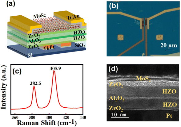
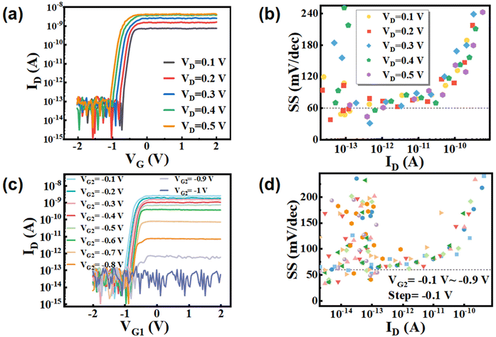
Fig. 1a schematically shows the structure of the MoS2 dual-gate FET device with HZO-involved gate dielectric stack. 12 nm HZO is sandwiched between the 2 nm ZrO2 capping layer and the 2 nm ZrO2 seed layer, and an additional 2 nm Al2O3 layer is inserted in the HZO layer. Such a crested symmetric structure can improve the remanent polarization (Fig. S2 and S3, ESI†) and tunneling electrical resistance ratio, and at the same time, it exhibits outstanding fatigue and retention characteristics.9,33,34 The dual gates are formed with Ti/Pt layers which are embedded in the SiO2 substrate. Ti/Au (10 nm/70 nm) metal layers are formed as the source/drain electrodes. Fig. 1b shows an optical microscopy image of a completed device. The Raman spectra of the MoS2 channel are shown in Fig. 1c. Fig. 1d illustrates a cross-sectional transmission electron microscopy (TEM) image of the device along the direction marked in Fig. 1b. A clear layered MoS2 channel and dielectric stack have been observed with sharp interfaces. The thickness of the MoS2 thin film is 2.9 nm corresponding to the thickness of 4 layers.As shown in Fig. 2a, the transfer characteristics with clear n-type behavior are achieved with the device. By increasing the gate 1 (G1) voltage VG1 from −2 V to 2 V, the drain-source voltage VDS increased from 100 mV to 500 mV, and the on/off ratio of the device is about 105 showing good switching behaviors. The device SS versus ID and VD voltage are shown in Fig. 2b, where the dashed line represents the Boltzmann constraint of 60 mV dec−1. Less than 60 mV dec−1 SS is clearly observed when the device is turned on, indicating that the device can effectively reduce the leakage current and power consumption, providing a solid basis for massive data processing. The counterclockwise switching is an intrinsic characteristic of the ferroelectric transistor.35–38 The hysteresis curves of the transfer characteristics are shown in Fig. S5 (ESI†).
Then, voltage is applied on gate 2 (G2) to study the dual-gate modulation. Fig. 2c shows the ID–VG1 curves when applying various VG2 pulses ranging from −0.1 to −1 V with a 0.1 V step. The on-state current decreases with VG2 up to −0.9 V, and remains off-state when VG2 drops beyond −1 V. This is because the barrier height of the channel region under the G2 coverage area increases with decreasing VG2, and the current thus continues to decrease. The relationship between SS and ID is shown in Fig. 2d, which confirms that the device under dual gate control can still maintain the low leakage current and power consumption. It is also noted that under the same VG1, different VG2 can regulate IDS in a wide range achieving dual-gate control. Fig. S6 (ESI†) illustrates the band diagram of the dual-gate MoS2 device under 2 gate control.
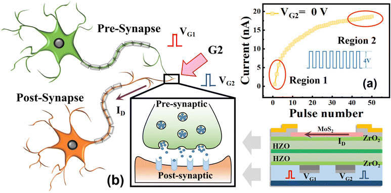
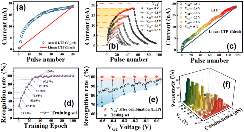
Fig. 3a shows the LTP characteristics of a single-gate-controlled device under continuous pulse. A total of 50 identical positive pulse sequences are applied on G1 (VG2 = 0). In region-1 under the initial stimulation of the pulse set, ID of the device exhibits a large change, and there are a few states. In the stimulation of the last few pulses (like in region-2), ID of the device can increase linearly and intensively with the increase in the number of pulses, and more importantly, the amount of conduction states in this stage is larger within the same current interval as compared to that in the initial stage. The same phenomenon is also evident in single gate devices. The optical microscope image, transfer characteristic curves and synaptic characteristics of the typical single-gate transistor are shown in Fig. S7 (ESI†). The ANN defined here uses the back propagation algorithm to continuously update the weights in the network training cycle. In the subsequent tests, the network weights will be replaced with the most recently connected conductance states after the mapping. In the replacement process, if the weight value falls in the more linear conductance state region, corresponding to the linear current brought by the rear pulse sequence namely region-2, the conductance state of this region increases linearly and densely, and the weight can be replaced more accurately with the conductance values. However, if the weight value corresponds to the conductance state caused by the initial pulse sequence, the linearity of the state will be degraded with a less number of conduction states. As a result, it is more difficult to define an accurate substitute conductance state, which will jeopardize the accuracy of the testing process below that of the network training leading to a lower recognition rate of the ANN. The LTD behavior of the device (VG2 = 0 V) under successive pulses is demonstrated in Fig. S8 (ESI†). Fig. 3b shows a schematic diagram of the biological synapses and the corresponding artificial synapse device. Corresponding to the device structure, the G1 electrode acts as a pre-synapse, which generates and transports electrical signals. The source and drain electrodes play the role of a post-synapse. The G2 electrode can be taken as a regulatory terminal which manipulates the channel current of the device together with G1.
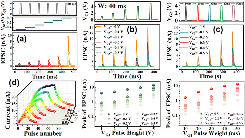
As shown in Fig. 4a, when a fixed voltage (4 V, 40 ms) is applied on G1 with various voltage biases on G2, ID also changes with VG2. As the voltage on G2 increases from −0.5 V to 0 V, ID also increases suggesting the regulating effect of G2 on G1. In order to further understand the regulating effect of G2 on G1 in this dual-gate device, we have separately studied the effects of VG1 pulses with different widths and amplitudes on ID under different VG2 pulses. Fig. 4b shows a schematic diagram of the excitatory post-synaptic current (EPSC) caused by a G1 spike and G2 control. VG1 with a pulse width of 40 ms and different amplitudes from 1 V to 5 V is applied to G1, and VDS remains at 600 mV. It can be seen that as the amplitude of VG1 increases under the same VG2, the corresponding max amplitude of ID gradually increases. Different VG2 pulses change the peak value of the EPSC under the same VG1 conditions, which indicates the regulating effect of G2. Similarly, as shown in Fig. 4c, the pulse width also has an impact on ID with increasing ID observed by increasing the pulse width from 10 ms to 50 ms (pulse amplitude = 4 V; VDS = 600 mV). It can also be seen that G2 regulates G1. The artificial neural network based on the double gate device is mainly used to simulate the recognition and classification of image data by the human brain. Mary Potter found that the human brain can recognize and understand a picture in 13–80 ms, and for the first time confirmed the fast processing ability of the human brain in the experiment.39 Meanwhile, the study also shows that although the brain only takes 13 ms to process image data, other parts of the brain continue to spend more time processing the image information. Therefore, as long as the response time of the device is less than 13 ms, the simulation of human brain image recognition can be realized. It can be seen that our double gate device can show a significant response to the pulse width of 10 ms, and the change of VG2 with the device response current is still very obvious. It provides a basis for our device to simulate the human brain for image recognition.
We then measured the LTP and LTD characteristics of the dual-gate device under different VG2. As demonstrated in Fig. 4d, continuous pulse (4 V) stimulation is applied on G1, and a constant small voltage (0 V to −0.5 V) is applied on G2 for regulation. In this way, six different sets of LTP/LTD curves are obtained. It can be seen that with the increase of VG2, the maximum ID increases significantly. However, for a fixed VG2 pulse, the device still exhibits non-linear LTP characteristics during the initial pulse sequence. However, it is worth mentioning that with the decrease of VG2, the sharp change in ID in the initial pulse stage is suppressed, which provides approaches for solving the non-linear issue. The paired pulse facilitation (PPF) characteristics of the dual-gate device are also studied, and are found to be consistent with the PPF phenomenon of neural synapses in biological systems (Fig. S9, ESI†).
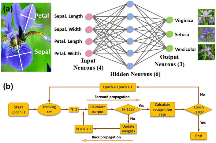
After confirming that the double gate device can simulate the neural synaptic behavior, an artificial neural network based on the double gate device is built. Fig. 5a illustrates the schematic diagram of a 3-layer network with 4 neurons in the input layer, 6 neurons in the hidden layer and 3 neurons in the output layer. We use the iris database to train the ANN. This database contains three types of irises: iris-setosa, iris-versicolour and iris-virginica (each kind with 50 sets of data, and 150 in total). Each data record contains four data items of the iris flower, namely the length of the sepal, the width of the sepal, the length of the petal, and the width of the petal, respectively, which correspond to the 4 input neurons of the neural network. The three types of irises correspond to 3 output neurons. In the ANN network training, 112 pieces of data in the database are used for training, the back propagation algorithm is used to update the weights after each training epoch, and the remaining 38 pieces of data are used to test the recognition rate of the network. Fig. 5b shows the flowchart of the training process. The calculation process of the neural network in detail is shown in Fig. S10 (ESI†) and the following discussion.
We use the correlation coefficient r to measure the fit degree between the two actual LTP curves and the ideal linear LTP curve:
Cov (actual LTP, ideal LTP) is the covariance of actual LTP and ideal LTP, Var [actual LTP] is the variance of actual LTP, and Var [ideal LTP] is the variance of ideal LTP. Among them, the closer r is to 1, the better the fitting degree is, which indicates that the linearity of LTP curve is better. By fitting the LTP curves in Fig. 6a, we found that under the condition of VG2 = 0, the correlation coefficient is 0.887.
In order to improve the correlation between the actual LTP curve and the current ideal curve, we adopted the method of combining LTP curves under different VG2 conditions. It is observed from Fig. 6b that in the LTP curve, with the decrease of the G2 voltage, the sudden change in ID in the initial pulse stage will be dampened, which is beneficial for improving the nonlinear issue. The method we adopt is to continuously increase the voltage on G2 as the number of pulses increases. This can not only alleviate the current sudden change in the initial stage of the pulse sequence, but also increase the adjustable range of the drain–source voltage, which enables more conductance values for the replacement of weights in the network. The specific G2 voltage change is shown by the red dotted line in the figure. Initially, G2 is applied with a constant voltage of −0.5 V, while G1 is continuously applied with the same pulse until ID reaches 4.93 nA. The voltage on G2 is increased to −0.4 V, and the G1 voltage is continuously applied with the same pulse until ID reaches 6.87 nA, followed by increasing the voltage on G2 to −0.3 V. Similarly, under continuous G1 pulses, when the current reaches 9.18 nA, 11.3 nA, and 14.8 nA, respectively, the voltage on G2 is increased to −0.2 V, −0.1 V and 0 V. The VG2 switching table is shown in Fig. S11 (ESI†). In this way, a combined LTP is obtained, and VG2 is also varied correspondingly which is named by V′G2. It can be clearly seen in Fig. 6c that the combined LTP curve LTP′ obtained through VG2 dynamic regulation is closer to the ideal curve. The correlation coefficient of LTP′ obtained through VG2 dynamic regulation reaches 0.996, which proves that the VG2 regulation can greatly improve the linearity of the LTP characteristics of the devices.
Fig. 6d shows that with the deep learning of the ANN, the recognition rate of the three irises continues to increases. The accuracy rate of the first training epoch is only 28.95%. As the number of training increases to 60 epochs, the recognition rate stabilizes at 100%. This shows that the ANN network we constructed has strong learning ability and a better recognition rate, which provides a solid basis for image classification and recognition. The weight value distribution changes with the number of training learning epochs (Fig. S12, ESI†).
For the LTP curve under a specific VG2, different conductance states are used to replace the weight value. The rule is that the conductance value and the ANN weight value are normalized in the same interval, and each weight value is replaced with the closest conductance value. In this way, for 7 sets of different VG2 pulses, 7 test recognition rates will be obtained as illustrated in Fig. 6e. Among them, the test recognition rate of the LTP curve obtained through different VG2 combinations can reach 100%, which is the same as the recognition rate of network training and learning. With the increase of gate voltage for the other six groups, the recognition rates were 68.42%, 73.68%, 81.58%, 84.21%, 86.84%, 92.11%, which are far lower than the recognition rates corresponding to V′G2. Therefore, the implementation of G2 in our dual-gate device structure can improve the recognition rate of iris flowers. Fig. S13 (ESI†) shows the comparison of the conductance continuous modulation process between the double gate device and the single gate device (VG2 = 0 V). The conductance state distribution corresponding to the weight value is shown in Fig. 6f.
Experimental
The device preparation process is shown in Fig. S14 (ESI†). The devices are prepared on a 300 nm SiO2/Si substrate. The dual-gate structure buried in SiO2 is patterned by ultraviolet lithography. The exposed SiO2 is removed with CHF3 reactive ion beam etching (RIE) followed by sputtering Ti/Pt films and a lift-off process. The gate stack is deposited in sequence on the buried gate structure using atomic layer deposition (ALD) at 300 °C. After that, 30 nm TiN film is grown by sputtering on the surface of the substrate which is further annealed at 550 °C for 35 s to form the ferroelectric phase in the HZO layer. The TiN metal layer is then removed by wet etching in a NH4OH![[thin space (1/6-em)]](https://www.rsc.org/images/entities/char_2009.gif) :
:![[thin space (1/6-em)]](https://www.rsc.org/images/entities/char_2009.gif) H2O2
H2O2![[thin space (1/6-em)]](https://www.rsc.org/images/entities/char_2009.gif) :
:![[thin space (1/6-em)]](https://www.rsc.org/images/entities/char_2009.gif) H2O solution (1
H2O solution (1![[thin space (1/6-em)]](https://www.rsc.org/images/entities/char_2009.gif) :
:![[thin space (1/6-em)]](https://www.rsc.org/images/entities/char_2009.gif) 1
1![[thin space (1/6-em)]](https://www.rsc.org/images/entities/char_2009.gif) :
:![[thin space (1/6-em)]](https://www.rsc.org/images/entities/char_2009.gif) 5). Channel material MoS2 thin film is then prepared by mechanical exfoliation from bulk crystals and is transferred and aligned with the dual gate region on the surface of the substrate. Subsequently, the source and drain are patterned by electron beam lithography (EBL). The contact electrodes Ti/Au (10 nm/70 nm) are formed by sputtering and the lift-off process similar to that of the dual-gate structure.
5). Channel material MoS2 thin film is then prepared by mechanical exfoliation from bulk crystals and is transferred and aligned with the dual gate region on the surface of the substrate. Subsequently, the source and drain are patterned by electron beam lithography (EBL). The contact electrodes Ti/Au (10 nm/70 nm) are formed by sputtering and the lift-off process similar to that of the dual-gate structure.
Conclusions
In conclusion, we propose a MoS2 dual-gate transistor based on the HZO crested symmetric structure. Among them, the HZO crested symmetric structure involves ZrO2 as the capping layer and seed layer, and Al2O3 as the interlayer to enhance the remanent polarization. On the one hand, the device reduces the sub-threshold swing of the device, and on the other hand, it improves the LTP non-linearity of the device by the regulation of two gates at the same time. We use the conductance state of the dual-gate device to replace all the weight values in the neural network, and the neural synapse based on this device used in the ANN shows a greatly enhanced recognition rate of iris flower reaching 100%, which is exactly the same as the accuracy of the network training. This has shown great potential in future device engineering for advanced artificial intelligence system applications.Conflicts of interest
There are no conflicts to declare.References
- C. Angermueller and T. Pärnamaa, Mol. Syst. Biol., 2016, 12, 878 CrossRef PubMed.
- G. Hinton, L. Deng, D. Yu, G. E. Dahl, A. Mohamed, N. Jaitly, A. Senior, V. Vanhoucke, P. Nguyen, T. N. Sainath and B. Kingsbury, IEEE Signal Process Mag., 2012, 29, 6 Search PubMed.
- K. Popper, Nature, 1968, 219, 5155 CrossRef.
- T. Wang, J. Meng and Z.-Y. He, Adv. Sci., 2020, 7, 8 Search PubMed.
- H. Zhang, T. J. Park and I. A. Zaluzhnyy, Nat. Commun., 2020, 11, 2245 CrossRef CAS PubMed.
- X. Yan, Z. Xiao and C. Lu, Appl. Phys. Lett., 2020, 116, 1 Search PubMed.
- G. Lee, J. H. Baek and F. Ren, Small, 2021, 17, 20 Search PubMed.
- M. Zhang, Z. Fan, X. Jiang, H. Zhu, L. Chen, Y. Xia, J. Yin, X. Liu, Q. Sun and D. W. Zhang, Nanophotonics, 2020, 9, 8 Search PubMed.
- Y. Liu, Y. Cao, H. Zhu, L. Ji, L. Chen, Q. Sun and D. W. Zhang, IEEE Electron Device Lett., 2021, 42, 9 Search PubMed.
- S. G. Yi, M. U. Park and S. H. Kim, ACS Appl. Mater. Interfaces, 2018, 10, 37 CrossRef PubMed.
- Y. Taur, IBM J. Res. Dev., 2002, 46, 23 Search PubMed.
- G. Fiori and F. Bonaccorso, Nat. Nanotechnol., 2014, 9(10), 768–779 Search PubMed.
- M. Chhowalla, D. Jena and H. Zhang, Nat. Rev. Mater., 2016, 1, 11 Search PubMed.
- R. Xu, H. Jang and M. H. Lee, Nano Lett., 2019, 19, 4 Search PubMed.
- S. J. Kim, J. Mohan, S. R. Summerfelt and J. Kim, JOM, 2018, 71, 1 Search PubMed.
- F. A. McGuire, Y. Lin, K. Price, G. B. Rayner, S. Khandelwal, S. Salahuddin and A. D. Franklin, Nano Lett., 2017, 17, 8 Search PubMed.
- J. Xu, S. Jiang, M. Zhang, H. Zhu, L. Chen, Q. Q. Sun and D. W. Zhang, Appl. Phys. Lett., 2018, 112, 103104 CrossRef.
- S. M. Dudek and M. F. Bear, Proc. Natl. Acad. Sci. U. S. A., 1992, 89, 10 Search PubMed.
- L. F. Abbott and S. B. Nelson, Nat. Neurosci., 2000, 3, 11 CrossRef PubMed.
- G. Rachmuth and H. Z. Shouval, Proc. Natl. Acad. Sci. U. S. A., 2011, 108, 49 CrossRef PubMed.
- G. Lee and J. H. Baek, Small, 2021, 17, 20 Search PubMed.
- B. Wang, X. Wang and E. Wang, Nano Lett., 2022, 21, 10400–10408 Search PubMed.
- L. Bao, J. Zhu and Z. Y. Jia, Appl. Mater. Interfaces, 2019, 11, 41482–41489 Search PubMed.
- Y. Wang, Y. Yang and Z. He, IEEE Electron Device Lett., 2020, 41, 9 Search PubMed.
- L. Wang, W. Liao and S. L. Wong, Adv. Funct. Mater., 2019, 29, 1901106 Search PubMed.
- H. Ryu, H. Wu and F. R., Sci. Rep., 2019, 9, 20383 CrossRef CAS PubMed.
- S. Wang, L. Liu, L. Gan, H. Chen, X. Hou, Y. Ding, S. Ma, D. W. Zhang and P. Zhou, Nat. Commun., 2021, 12, 1 CrossRef PubMed.
- T. Wang, J. Meng and Z. He, Nanoscale Horiz., 2019, 4, 1293 RSC.
- X. Zhu, D. Li, X. Liang and W. D. Lu, Nat. Mater., 2019, 18, 141 CrossRef CAS PubMed.
- Y. Chen, Y. Zhou, F. Zhuge, B. Tian, M. Yan, Y. Li, Y. He and X. S. Miao, npj 2D Mater. Appl., 2019, 5, 3 CrossRef CAS.
- V. K. Sangwan, H. S. Lee, H. Bergeron, I. Balla, M. E. Beck, K. S. Chen and M. C. Hersam, Nature, 2018, 554, 500 CrossRef CAS PubMed.
- T. Wang, J. Meng, M. Rao, Z. Y. He, L. Chen, H. Zhu, Q. Sun, S. J. Ding, W. Z. Bao, P. Zhou and D. W. Zhang, Nano Lett., 2020, 20, 6 Search PubMed.
- J. Wang, IEEE Electron Device Lett., 2019, 40, 12 CAS.
- T. Onaya, Appl. Phys. Express, 2017, 10, 8 Search PubMed.
- T. Ali, P. Polakowski and S. Riedel, IEEE Trans. Electron Devices, 2018, 65, 3769–3774 CAS.
- T. Ali, P. Polakowski and S. Riedel, Appl. Phys. Lett., 2018, 112, 222903 Search PubMed.
- W. Xiao, C. Liu and Y. Peng, Nanoscale Res. Lett., 2019, 14, 245 CrossRef PubMed.
- B. J. Zeng, M. Liao and Q. X. Peng, IEEE J. Electron Devices Soc., 2019, 7, 551–556 CAS.
- M. C. Potter, B. Wyble and C. E. Hagmann, Atten. Percept. Psychophys., 2013, 76, 270–279 Search PubMed.
Footnote |
| † Electronic supplementary information (ESI) available. See DOI: https://doi.org/10.1039/d2nr05720d |
| This journal is © The Royal Society of Chemistry 2023 |

