Highly anisotropic and ultra-diffusive vacancies in α-antimonene†
Ning
Lu
 *a,
Xin
Hu
a,
Jiaxin
Jiang
a,
Hongyan
Guo
a,
Gui Zhong
Zuo
b,
Zhiwen
Zhuo
 *a,
Xiaojun
Wu
 c and
Xiao Cheng
Zeng
 *d
*d
aAnhui Province Key Laboratory of Optoelectric Materials Science and Technology, Key Laboratory of Functional Molecular Solids Ministry of Education, Anhui Laboratory of Molecule-Based Materials, and Department of Physics, Anhui Normal University, Wuhu, Anhui 241000, China. E-mail: luning@ahnu.edu.cn; zhuozw@ustc.edu.cn
bInstitute of Plasma Physics, HIPS, Chinese Academy of Sciences, Hefei, 230031, China
cHefei National Laboratory for Physical Sciences at the Microscale, CAS Key Laboratory of Materials for Energy Conversion, and School of Chemistry and Materials Sciences, University of Science and Technology of China, Hefei, Anhui 230026, China
dDepartment of Materials Science & Engineering, City University of Hong Kong, Kowloon, 999077, Hong Kong. E-mail: xzeng26@cityu.edu.hk
First published on 16th February 2023
Abstract
α-Antimonene has recently been successfully fabricated in experiment; hence, it is timely to examine how various types of point defects in α-antimonene can affect its novel electronic properties. Herein, we present a comprehensive investigation of a total of nine possible types of point defects in α-antimonene via first-principles calculations. Particular attention is placed on the structural stability of the point defects and the effects of point defects on the electronic properties of α-antimonene. Compared with its structural analogs, such as phosphorene, graphene, and silicene, we find that most defects in α-antimonene can be more easily generated, and that among the nine types of point defects, the single vacancy SV-(5|9) is likely the most stable one while its presence can be orders of magnitude higher in concentration than that in phosphorene. Moreover, we find that the vacancy exhibits anisotropic and low diffusion barriers, of merely 0.10/0.30 eV in the zigzag/armchair direction. Notably, at room temperature, the migration of SV-(5|9) in the zigzag direction of α-antimonene is estimated to be three orders faster than that along the armchair direction, and also three orders faster than that of phosphorene in the same direction. Overall, the point defects in α-antimonene can significantly affect the electronic properties of the host two-dimensional (2D) semiconductor and thus the light absorption capability. The anisotropic, ultra-diffusive, and charge tunable single vacancies, along with the high oxidation resistance, render the α-antimonene sheet a unique 2D semiconductor (beyond the phosphorene) for developing vacancy-enabled nanoelectronics.
Introduction
Owing to their anisotropic structures and novel functional properties, group-V elemental nanomaterials have attracted intense interests.1–6 In particular, phosphorene, a single-layer black phosphorous, possesses an intrinsically tunable direct bandgap (∼1.56 eV),7 high carrier mobility (1.0–2.6 × 104 cm2 V−1 s−1),8 flexible mechanical properties, and anisotropic electrical, optical, and thermal transport properties, thereby having potential for various applications, e.g., flexible nano-devices in nanoelectronics, optoelectronics, thermoelectrics, and photocatalysts, etc.9–12 However, due to the poor chemical stability, phosphorene can be easily oxidized and degraded in open air.13,14 Thus, coating protection of phosphorene should be required for its application in various devices. A structural analog of phosphorene with higher chemical stability would be highly desired. Recently, stable BP-like α-antimonene was successfully synthesized on different substrates, such as Td-WTe2, Td-MoTe2, SnSe, etc.15–18Compared with phosphorene, the α-antimonene not only possesses similar anisotropic mechanical, electrical and transport properties, along with a strain-tunable band gap (0.2 eV) and high ZT values, but also exhibits a two orders higher carrier mobility (1.4 × 106 cm2 V−1 s−1) and a higher electrical conductivity, as well as excellent chemical stability in air.19–23Like bulk materials, intrinsic point defects can be also present in 2D materials. Hence, the defect-dependent structural, physical, and chemical properties can be exploited for various applications, e.g., electrocatalytic hydrogen evolution, gas sensors, spintronics, multiferroics, memristive devices, etc.24–36 For 2D elemental materials (e.g., phosphorene, graphene, and silicene) with honeycomb-like structures, known point defects include the Stone–Wales (SW), single vacancy (SV), and double vacancy (DV) defects, which have been extensively investigated.24,25,37–40 Among them, the SW defect has been viewed as the most popular defect in 2D elemental sheets because it generally entails the lowest formation energy (Ef).41 In graphene and silicene, the DV can be much more easily generated than SV, whereas in phosphorene, the opposite trend prevails. Moreover, the concentration of all three types of point defects is much higher in phosphorene than in silicene and graphene, again due to the significantly lower vacancy formation energy (Ef) in the former. For example, Ef of SV is 1.63 eV (phosphorene)41 <3.77 eV (graphene)24 <7.80 eV (silicene).25
Note that the diffusion of SV in phosphorene is 16 orders of magnitude faster than that in graphene at room temperature due to the much lower diffusion barrier of Eb = 0.4 eV for phosphorene (vs. 1.39 eV for graphene). In addition, the diffusion barriers are strikingly adjustable (by ∼0.2 eV) through in-plane strain, allowing strain engineering of defect motion.29 Indeed, owing to its highly mobile SV, phosphorene has been considered as a promising candidate for vacancy-enabled nanodevices, e.g., memristive devices, via strain engineering and defect manipulation.29 For α-antimonene, its point defects have been indirectly measured in experiment once the defects can be clasped by adsorbates.15 However, the structural properties of various point defects in α-antimonene, their likelihood of occurrence, and their diffusivity at room temperature are still largely unexplored.42
In this work, the structural properties and thermal stability of typical point defects in α-antimonene, as well as the influence of defects on the electronic structure and on the light absorption are systematically studied by using first-principles computation and ab initio molecular dynamics simulations. Compared with phosphorene, graphene, and silicene, we find that the same type of point defects can be more easily generated in α-antimonene. The point defects can be mostly distinguished through simulated scanning tunneling microscopy (STM) imaging. Notably, we find that the defects can have a marked influence on the electronic and optical properties of α-antimonene. Among the point defects, the SV-(5|9) defect is predicted to be the most stable and it has the lowest formation energy, hence the highest concentration. Furthermore, the diffusion of the SV-(5|9) defect appears to be anisotropic and ultra-mobile as the diffusion barrier of SV-(5|9) is merely 0.10–0.30 eV. The charge injection is an alternative means to enhance the controllability of the vacancies via an electric field and to develop vacancy-enabled electronics applications.
Results and discussion
Geometric structure of α-antimonene and stability of point defects
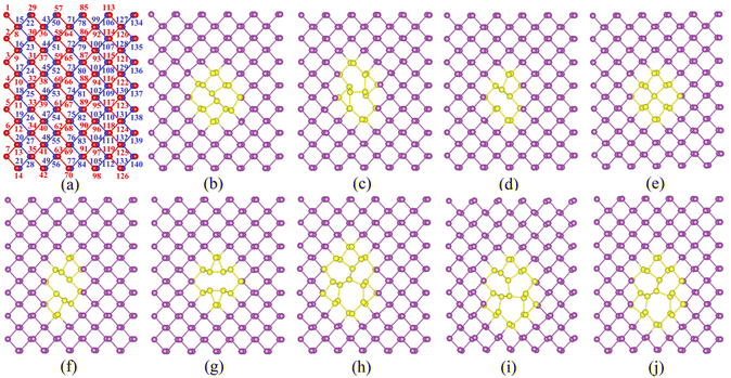
The structure of α-antimonene (5 × 7 × 1 supercell) is shown in Fig. 1a and Fig. S1 (ESI).† The lattice constants are a = 4.36 Å and b = 4.74 Å, in agreement with those reported in a previous study (a = 4.36 Å, b = 4.73 Å).43 In Fig. 1a, all Sb atoms are marked with numbers, where the red and blue balls represent the Sb atoms in the upper and lower layers, respectively. Structures of nine types of defects in α-antimonene are illustrated in Fig. 1b–j, including two types of SW (denoted as SW-1 and SW-2), two types of SV (denoted as SV-(5|9) and SV-(55|66)), and five types of double-vacancy DV-(555|777) (denoted as DV-(5|8|5), DV-(4|10|4), DV-(555|777)-1, DV-(555|777)-2, and DV-(555|777)-3) defects after structure optimization. Compared with graphene and silicene, the low symmetry α-antimonene entails more varieties of point defects like phosphorene (as similar defective structures have been created in the previous study41). In Fig. 1b and c, SW-1 and SW-2 defects are generated via rotating Sb(67)–Sb(74) and Sb(60)–Sb(67) pairs by 90°, respectively. In Fig. 1c and d, both SV defects are generated by removing Sb(67) atoms but within different reconstructions; namely, inclined Sb(74) to generate the SV-(5|9) defect and central Sb(74) to generate the SV-(55|66) defect. Among the five DV defects in α-antimonene, as shown in Fig. 1f and g, the DV-(5|8|5) defect is generated by removing the Sb(61)–Sb(67) pair, and the DV-(4|10|4) defect is produced by removing the Sb(67)–Sb(74) pair. The three other DV structures all belong to DV-(555|777), which are more complicated. As shown in Fig. 1h–j, different from DV-(5|8|5) and DV-(4|10|4), DV-(555|777)-1, DV-(555|777)-2 and DV-(555|777)-3 defects are generated by removing two non-bonding Sb atoms, Sb(54) and Sb(60), or Sb(67) and Sb(68), or Sb(61) and Sb(75), respectively.To evaluate the stability of various defects in α-antimonene, the formation energy of defects is calculated according to the formula:
| Ef = Etot − NSb × ESb |
| E f | E g | |
|---|---|---|
| Perfect | 0.00 | 0.20 |
| SW-1 | 1.12 | 0.12 |
| SW-2 | 1.61 | 0.16 (Indirect) |
| SV-(5|9) | 0.97 | Metal |
| SV-(55|66) | 0.99 | Metal |
| DV-(5|8|5) | 1.16 | 0.11 |
| DV-(4|10|4) | 1.07 | 0.11 |
| DV-(555|777)-1 | 2.33 | 0.11 |
| DV-(555|777)-2 | 2.65 | 0.11 |
| DV-(555|777)-3 | 2.34 | 0.07 |
The thermal stability of defective α-antimonene is investigated by using ab initio molecular dynamics (AIMD) simulations with the temperature being controlled at 300 K, 400 K, and 800 K, respectively. As shown in Fig. S2–S4 (ESI),† at 300 K and 400 K, the SW-1 and SW-2 defects can spontaneously transform into the perfect α-antimonene structure. SV-(55|66) can transform into SV-(5|9) after 5 ps MD simulation, while the SV-(5|9) can be stable after 5 ps AIMD simulation. For DV defects, all defective structures except the DV-(555|777)-3 defect appear to be thermally stable after 5 ps simulation. At a much higher temperature of 800 K, the SW-1 defect still spontaneously transforms into the perfect α-antimonene. SV-(5|9) and DV-(5|8|5) can survive after 5 ps AIMD simulation at 800 K, while other defective structures undergo considerable reconstruction after 5 ps simulation. Thus, the SV-(5|9) defect is likely a stable configuration at room temperature, which may be detectable in experiment.
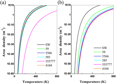
For the perfect α-antimonene and phosphorene, the areal densities of the number of the atoms are Nperfect(antimonene) = 1.94 × 10¹⁹ atom per m2 and Nperfect(phosphorene) = 2.62 × 10¹⁹ atom per m2, respectively.41 At a finite temperature, the areal density of the number of atoms of defects (Ndefect) in a 2D material can be estimated via the Arrhenius equation:
| Ndefect = Nperfectexp(−Ef/kBT) |
Diffusion barrier of SV in α-antimonene
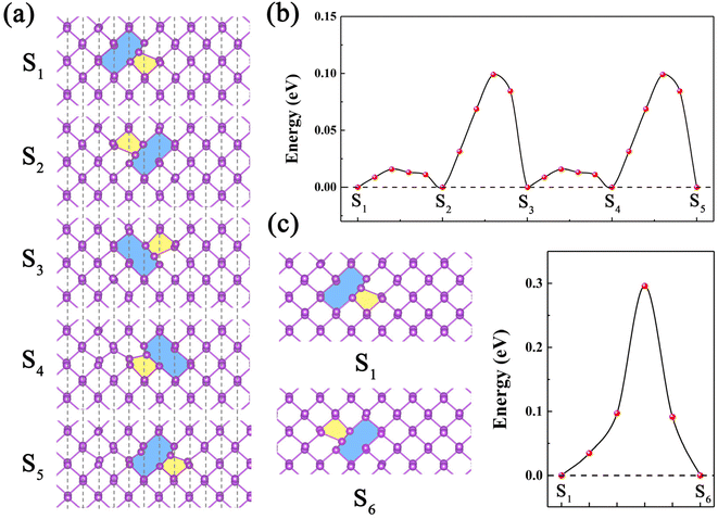
The defects can migrate or transform among one another at finite temperatures. Thus, it is important to investigate temperature-dependent diffusion behavior of the defects. Here, the diffusion behavior of the most stable SV-(5|9) defect is investigated. Due to the anisotropic structure of α-antimonene, two possible diffusion paths of SV-(5|9) are considered, including the intrachain diffusion path (along the zigzag direction) and the interchain diffusion path (along the armchair direction). The combination of the two paths allows an analysis of the diffusion behavior of SV in any direction within the sheet. For the intrachain diffusion of SV-(5|9) along the zigzag direction, the sequential steps (S1 → S2 → … → S5) and the corresponding energy landscapes are plotted in Fig. 3a and b. For the diffusion steps of S1 → S2 and S3 → S4, the energy barrier is 0.02 eV. For S2 → S3 and S4 → S5, the energy barrier of the rate-limiting step is only 0.10 eV. For the interchain diffusion of SV-(5|9), the energy barrier of the rate-limiting step (S1 → S6) is 0.30 eV, as shown in Fig. 3c. Thus, the diffusion of SV-(5|9) in α-antimonene is anisotropic, with a 0.10 eV energy barrier in the zigzag direction vs. a 0.30 eV energy barrier in the armchair direction (referred to as the 0.10/0.30 eV energy barrier in the zigzag/armchair direction).The diffusion energy barrier of SV-(5|9) for α-antimonene (0.10/0.30 eV energy barrier in the zigzag/armchair direction) is lower than that for phosphorene (0.3/0.4 eV energy barrier in the zigzag/armchair direction),29 and much lower than that for graphene (1.39 eV), MoS2 (VS, 2.27 eV), and BN (VB, 2.60 eV). The hopping rate can be calculated from the Arrhenius formula v = vs exp(−Eb/kBT), where vs is the characteristic frequency, normally around 1013 Hz, kB is the Boltzmann constant, and T is the temperature.29 At room temperature, the migration of SV-(5|9) in α-antimonene and in the zigzag direction is estimated to be three orders faster than that in the armchair direction, and exhibits high anisotropy. In addition, the migration of SV-(5|9) in α-antimonene and in the zigzag direction is estimated to be three orders of magnitude faster than that of phosphorene in the same direction at room temperature (RT). Moreover, the migration of SV-(5|9) in α-antimonene and in the armchair direction is estimated to be one order of magnitude faster than that in phosphorene, and 18 orders of magnitude faster than that in graphene and in the same direction at RT. These results indicate that SV-(5|9) in α-antimonene is more feasible for vacancy migration, compared with phosphorene. Further AIMD simulation of SV-(5|9) at 300 K confirms that a number of hopping events occurred in the zigzag direction within 5 ps (see Movie S1 and Fig. S6, ESI†), consistent with the low diffusion energy barrier in the zigzag direction. Therefore, SV-(5|9) in α-antimonene exhibits highly anisotropic diffusivity and mobile motion.
In addition to strain engineering mentioned in the previous study,29 finding more ways to manipulate the motion of point defects is very important for practical applications. The mobile defects with dipoles or with local charge are directionally migratable under an external electric field. For example, in memristive materials,33,36 an electric field can be exploited as an effective manipulation method to control point defect behavior. According to our calculation under charge-neutral conditions, the total charge of Sb atoms around the SV-(5|9) defect is 0.07e per vacancy (involving 14 Sb atoms), where the highest charge of a neighboring Sb atom is 0.06e, as shown in Fig. S7 (ESI).† The vacancies with few charges may be detectable and drivable in an electric field for vacancy-enabled nanoelectronics applications. Moreover, the defect possesses an intrinsic electric dipole due to its specific shape so that the defect can be manipulated by an external electric field. Furthermore, charge injection can be used as a way to enhance the capability of electric field manipulation of the defects. For instance, under the condition of negative charge injection with a concentration of 1e per SV-(5|9), the extra charge tends to locate around the SV-(5|9) defect. As a result, the local charge can rise to 0.19e per vacancy, and the highest charge associated with a neighboring Sb atom can amount to 0.09e. On the other hand, for positive charge injection, the total charge around the defect is reduced to −0.01e per vacancy. Thus, the negative charge injection can be useful to strengthen the controllability of defect motion.
Influence of point defects on electronic and optical properties of α-antimonene
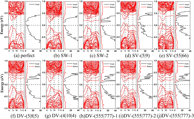
The computed electronic structures of α-antimonene with or without point defects are shown in Fig. 4a–j, respectively. As shown in Fig. 4a, the band structure of the perfect α-antimonene exhibits a direct band gap of 0.2 eV, consistent with the previous theoretical study43 and the experimental value of 0.17 eV.17 Like the perfect α-antimonene, α-antimonene with the SW-1 defects is predicted to be the direct band gap semiconductor (Fig. 4b) with a reduced band gap of 0.12 eV (see Table 1). For the α-antimonene with SW-2 defects, the band gap becomes an indirect one with a value of 0.16 eV (Fig. 4c). Fig. 4d and e shows that the α-antimonene with SV-(5|9) or SV-(55|66) point defects exhibits metallic characters with hole doping due to the odd number of electrons in the system. These distinctly different electronic structures are helpful for applications, e.g., to distinguish different areas with a different density of vacancies.As shown in Fig. 4f–j, the DV defects result in direct band gap semiconductors for α-antimonene, but the band gap is significantly reduced to ∼0.1 eV. Among them, α-antimonenes with DV-(5|8|5), DV-(4|10|4), DV-(555|777)-1, or DV-(555|777)-2 defects all have a band gap of ∼0.11 eV, while that with DV-(555|777)-3 defects has an even smaller band gap of 0.07 eV. Therefore, the presence of the point defects can markedly affect the electronic properties of α-antimonene.
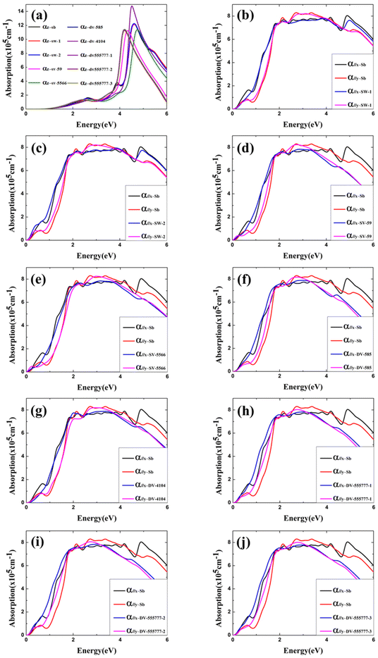
Optical properties of α-antimonene without and with point defects are also computed (see detailed results in ESI†). As shown in Fig. 5a, for incident light polarized along the z-axis (α//z), the optical absorption coefficient (α) of both the perfect α-antimonene and the defective α-antimonene exhibits strong light absorption in the ultraviolet region. As shown in Fig. 5b–j, for incident light polarized along the x-axis (α//x) and y-axis (α//y), both the perfect α-antimonene and the defective α-antimonene exhibit strong light absorption properties in the visible light region. Fig. 5b and c shows that the optical absorption of α-antimonene with SW-1 and SW-2 defects is similar to that of perfect α-antimonene. The absorption edge for α-antimonene with SV-(5|9) and SV-(55|66) appears red-shifted due to the semiconductor-to-metal transition (Fig. 5d and e). For DV defects, the absorption of ultraviolet light in the 4–6 eV range is generally weakened. However, α-antimonene with DV-(5|8|5) and DV-(555|777) class of defects results in stronger absorption of near-infrared light in the 0–2 eV range.
Simulated STM images of α-antimonene point defects
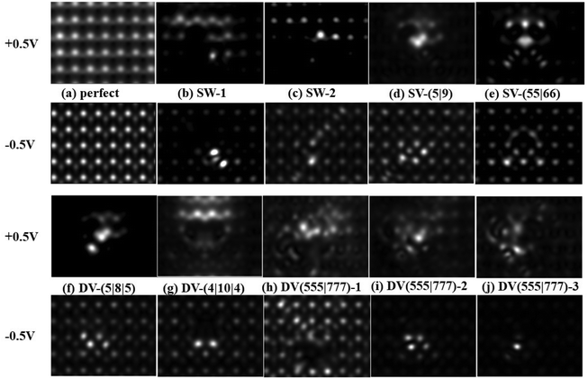
To assist experimental identification of different types of point defects in future experiments, the simulated scanning tunneling microscopy (STM) images of the perfect and defective α-antimonene under +0.5 V and −0.5 V bias are shown in Fig. 6. As shown in the upper panels of Fig. 6c–g, the SW-2, SV-(5|9), SV-(55|66), DV-(5|8|5), and DV-(4|10|4) defects can be distinguished more easily under a positive bias (+0.5 V). Specifically, the STM images of SW-2, SV-(5|9), and DV-(5|8|5) exhibit one large and one small bright spot, a small group of bright spots, and two small bright spots on the same diagonal, respectively. The SV-(55|66) defect gives rise to a symmetric bright spot pattern, corresponding to the structure of the defect. The DV-(4|10|4) defect gives rise to a light spot surrounding a black area with two wide ends and a narrow middle, highly similar to its defective structure. As shown in the lower part of Fig. 6b and h–j, SW-1, DV-(555|777)-2, and DV-(555|777)-3 defects can be distinguished more easily under a negative bias (−0.5 V). The STM image of SW-1, DV-(555|777)-2, and DV-(555|777)-3 defects is displayed as two bright spots, four bright spots, and one bright spot, respectively.Conclusions
Nine types of point defects in α-antimonene are systematically studied by using density functional theory and ab initio molecular dynamics simulation. These point defects include SW-1, SW-2, SV-(5|9), SV-(55|66), DV-(5|8|5), DV-(555|777)-1, DV-(555|777)-2, DV-(555|777)-3, and DV-(4|10|4). Among the nine defects, the formation energy of the SV-(5|9) defect is the lowest. Moreover, α-antimonene appears to have an areal density of the SV-(5|9) defects orders higher than that of phosphorene at same temperature. AIMD simulations indicate that SW-1, SW-2, and SV-(55|66) defects are unstable at room temperature, while the other defective structures are thermally stable at room temperature. The diffusion of SV-(5|9) exhibits strong anisotropic character with the diffusion barrier of 0.10/0.30 eV along the zigzag/armchair direction, notably lower than that (0.3/0.4 eV) for phosphorene. The charge injection can be a useful means to strengthen the controllability of the defect motion and manipulation via an electric field. The presence of the defects also has a marked effect on the electronic and optical properties of α-antimonene. In particular, the SV-(5|9) defect results in the metallic character of hole doping for α-antimonene, making the SV-(5|9) defect easier to be detected in experiments and manipulated, compared with phosphorene. Furthermore, most point defects of different types can be easily distinguished from one another through scanning tunneling microscopy measurements. Our study provides helpful guidance in the identification of various point defects in α-antimonene, and new insights into defect formation, defect diffusion behavior, as well as the effect of various defects on the electronic and optical properties. Overall, the novel defect-related properties of α-antimonene, including anisotropic, ultra-diffusive, and charge adjustable vacancies, render α-antimonene a potential 2D semiconductor for designing vacancy-enabled low-dimensional electronic devices.Computational details
All calculations are performed within the framework of density-functional theory (DFT), implemented in the Vienna ab initio simulation package (VASP 5.4).45,46 Among them, the exchange correlation functional is the PBE method of generalized gradient approximation,47 which has previously proven to describe the electronic structure of 2D α-antimonene, phosphorene,48 graphene24 and silicene25 well. By using the conjugate gradient algorithm, all atomic coordinates are fully relaxed until the total energy and atomic force converge to 10−5 eV and 10−2 eV Å−1, respectively. To study the influence of various point defects in α-antimonene, a 5 × 7 α-antimonene (140 antimony (Sb) atoms) superlattice is used, and a 15 Å vacuum layer is added in the Z direction to eliminate the influence between the crystal layer and its image layers. In the calculations, a plane-wave basis with a cutoff energy of 500 eV is selected to expand the electronic wave function, and the k-point sampling is carefully examined to assure that the calculation results are converged. To examine the thermal stability of the 2D α-antimonene structure, ab initio molecular dynamics (AIMD) simulations are performed on the selected system. The AIMD simulations are carried out in the canonic ensemble, and the total simulation time is 5.0 ps, while the time step is set to 1.0 fs. The temperature is controlled at 300 K, 400 K and 800K, respectively. The diffusion energy barriers are calculated based on the climbing image nudged elastic band (CI-NEB) method.49Conflicts of interest
The authors declare no competing financial interest.Acknowledgements
NL and ZZ were supported by the Anhui Provincial Natural Science Foundation (No. 2208085QA11 and No. 2008085QA33), the University Annual Scientific Research Plan of Anhui Province (No. 2022AH010013) and the Hefei Advanced Computing Center. GZZ was supported by the National Natural Science Foundation of China (No. 11775261). XCZ acknowledges the support by the Hong Kong Global STEM Professorship Scheme.References
- T. Niu, J. Zhang and W. Chen, ChemNanoMat, 2019, 5, 6–23 CrossRef CAS.
- S. Zhang, M. Xie, F. Li, Z. Yan, Y. Li, E. Kan, W. Liu, Z. Chen and H. Zeng, Angew. Chem., Int. Ed., 2016, 55, 1666–1669 CrossRef CAS PubMed.
- P. Ares, J. J. Palacios, G. Abellán, J. Gómez-Herrero and F. Zamora, Adv. Mater., 2018, 30, 1703771 CrossRef PubMed.
- A. A. Kistanov, D. R. Kripalani, Y. Cai, S. V. Dmitriev, K. Zhou and Y.-W. Zhang, J. Mater. Chem. A, 2019, 7, 2901–2907 RSC.
- D. R. Kripalani, A. A. Kistanov, Y. Cai, M. Xue and K. Zhou, Phys. Rev. B, 2018, 98, 085410 CrossRef CAS.
- M. Pumera and Z. Sofer, Adv. Mater., 2017, 29, 1605299 CrossRef PubMed.
- V. Wang, Y. Kawazoe and W. T. Geng, Phys. Rev. B: Condens. Matter Mater. Phys., 2015, 91, 045433 CrossRef.
- J. Qiao, X. Kong, Z.-X. Hu, F. Yang and W. Ji, Nat. Commun., 2014, 5, 4475 CrossRef CAS PubMed.
- L. Li, Y. Yu, G. J. Ye, Q. Ge, X. Ou, H. Wu, D. Feng, X. H. Chen and Y. Zhang, Nat. Nanotechnol., 2014, 9, 372–377 CrossRef CAS PubMed.
- S. Lin, S. Liu, Z. Yang, Y. Li, T. W. Ng, Z. Xu, Q. BaO, J. Hao, C. S. Lee and C. Surya, Adv. Funct. Mater., 2016, 26, 864–871 CrossRef CAS.
- G. Long, D. Maryenko, J. Shen, S. Xu, J. Hou, Z. Wu, W. K. Wong, T. Han, J. Lin and Y. Cai, Nano Lett., 2016, 16, 7768–7773 CrossRef CAS PubMed.
- S. Zhang, S. Guo, Z. Chen, Y. Wang, H. Gao, J. Gómez-Herrero, P. Ares, F. Zamora, Z. Zhu and H. Zeng, Chem. Soc. Rev., 2018, 47, 982–1021 RSC.
- J. D. Wood, S. A. Wells, D. Jariwala, K.-S. Chen, E. Cho, V. K. Sangwan, X. Liu, L. J. Lauhon, T. J. Marks and M. C. Hersam, Nano Lett., 2014, 14, 6964–6970 CrossRef CAS PubMed.
- Z. Hu, Q. Li, B. Lei, Q. Zhou, D. Xiang, Z. Lyu, F. Hu, J. Wang, Y. Ren, R. Guo, E. Goki, L. Wang, C. Han, J. Wang and W. Chen, Angew. Chem., Int. Ed., 2017, 56, 9131–9135 CrossRef CAS PubMed.
- Z.-Q. Shi, H. Li, Q.-Q. Yuan, Y.-H. Song, Y.-Y. Lv, W. Shi, Z.-Y. Jia, L. Gao, Y.-B. Chen, W. Zhu and S.-C. Li, Adv. Mater., 2019, 31, 1806130 CrossRef PubMed.
- Z.-Q. Shi, H. Li, Q.-Q. Yuan, C.-L. Xue, Y.-J. Xu, Y.-Y. Lv, Z.-Y. Jia, Y. Chen, W. Zhu and S.-C. Li, ACS Nano, 2020, 14, 16755–16760 CrossRef CAS PubMed.
- Z.-Q. Shi, H. Li, C.-L. Xue, Q.-Q. Yuan, Y.-Y. Lv, Y.-J. Xu, Z.-Y. Jia, L. Gao, Y. Chen, W. Zhu and S.-C. Li, Nano Lett., 2020, 20, 8408–8414 CrossRef CAS PubMed.
- C. Hogan, K. Holtgrewe, F. Ronci, S. Colonna, S. Sanna, P. Moras, P. M. Sheverdyaeva, S. Mahatha, M. Papagno, Z. S. Aliev, M. Babanly, E. V. Chulkov, C. Carbone and R. Flammini, ACS Nano, 2019, 13, 10481–10489 CrossRef CAS PubMed.
- D. Singh, S. K. Gupta, T. Hussain, Y. Sonvane, P. N. Gajjar and R. Ahuja, Energy Fuels, 2021, 35, 9001–9009 CrossRef CAS.
- T. Bo, Y. Liu, J. Yuan, P. Wu and W. Zhou, Appl. Surf. Sci., 2020, 507, 145194 CrossRef CAS.
- Y. Guo, H. Zhu and Q. Wang, J. Phys. Chem. C, 2020, 124, 5506–5513 CrossRef CAS.
- G. Wang, R. Pandey and S. P. Karna, ACS Appl. Mater. Interfaces, 2015, 7, 11490–11496 CrossRef CAS PubMed.
- Y. Wu, K. Xu, C. Ma, Y. Chen, Z. Lu, H. Zhang, Z. Fang and R. Zhang, Nano Energy, 2019, 63, 103870 CrossRef CAS.
- F. Banhart, J. Kotakoski and A. V. Krasheninnikov, ACS Nano, 2011, 5, 26–41 CrossRef CAS PubMed.
- J. Gao, J. Zhang, H. Liu, Q. Zhang and J. Zhao, Nanoscale, 2013, 5, 9785–9792 RSC.
- O. Leenaerts, B. Partoens and F. M. Peeters, Appl. Phys. Lett., 2008, 93, 193107 CrossRef.
- W. Hu, X. Wu, Z. Li and J. Yang, Nanoscale, 2013, 5, 9062–9066 RSC.
- W. Hu, X. Wu, Z. Li and J. Yang, Phys. Chem. Chem. Phys., 2013, 15, 5753–5757 RSC.
- Y. Cai, Q. Ke, G. Zhang, B. I. Yakobson and Y.-W. Zhang, J. Am. Chem. Soc., 2016, 138, 10199–10206 CrossRef CAS PubMed.
- T. Hu and J. Dong, Nanotechnology, 2015, 26, 065705 CrossRef CAS PubMed.
- R. Babar and M. Kabir, J. Phys. Chem. C, 2016, 120, 14991–15000 CrossRef CAS.
- J. Kerski, P. Lochner, A. Ludwig, A. D. Wieck, A. Kurzmann, A. Lorke and M. Geller, Phys. Rev. Appl., 2021, 15, 024029 CrossRef CAS.
- M. Lübben, F. Cüppers, J. Mohr, M. von Witzleben, U. Breuer, R. Waser, C. Neumann and I. Valov, Sci. Adv., 2020, 6, eaaz9079 CrossRef PubMed.
- X. Tong, Y. Zhao, Z. Zhuo, Z. Yang, S. Wang, Y. Liu, N. Lu, H. Li and T. Zhai, Angew. Chem., Int. Ed., 2022, 61, e202112953 CAS.
- Q. Yang, W. Xiong, L. Zhu, G. Gao and M. Wu, J. Am. Chem. Soc., 2017, 139, 11506–11512 CrossRef CAS PubMed.
- K. C. Kwon, J. H. Baek, K. Hong, S. Y. Kim and H. W. Jang, Nano-Micro Lett., 2022, 14, 58 CrossRef CAS PubMed.
- A. Hashimoto, K. Suenaga, A. Gloter, K. Urita and S. Iijima, Nature, 2004, 430, 870–873 CrossRef CAS PubMed.
- R. G. Amorim, A. Fazzio, A. Antonelli, F. D. Novaes and A. Silva, Nano Lett., 2007, 7, 2459–2462 CrossRef CAS PubMed.
- L. Kou, C. Tang, W. Guo and C. Chen, ACS Nano, 2011, 5, 1012–1017 CrossRef CAS PubMed.
- H. Sahin, J. Sivek, S. Li, B. Partoens and F. M. Peeters, Phys. Rev. B: Condens. Matter Mater. Phys, 2013, 88, 7795–7799 CrossRef.
- W. Hu and J. Yang, J. Phys. Chem. C, 2015, 119, 20474–20480 CrossRef CAS.
- Y. Liu, F. Xu, Z. Zhang, E. S. Penev and B. I. Yakobson, Nano Lett., 2014, 14, 6782–6786 CrossRef CAS PubMed.
- Y. Xu, B. Peng, H. Zhang, H. Shao, R. Zhang, H. Lu, D. W. Zhang and H. Zhu, Ann. Phys., 2017, 529, 1600152 CrossRef.
- J. M. H. Kroes, M. A. Akhukov, J. H. Los, N. Pineau and A. Fasolino, Phys. Rev. B: Condens. Matter Mater. Phys, 2011, 83, 165411 CrossRef.
- G. Kresse and J. Furthmüller, Phys. Rev. B: Condens. Matter Mater. Phys, 1996, 54, 11169–11186 CrossRef CAS PubMed.
- G. Kresse and D. Joubert, Phys. Rev. B: Condens. Matter Mater. Phys, 1999, 59, 1758–1775 CrossRef CAS.
- J. P. Perdew, K. Burke and M. Ernzerhof, Phys. Rev. Lett., 1996, 77, 3865–3868 CrossRef CAS PubMed.
- H. Guo, N. Lu, J. Dai, X. Wu and X. C. Zeng, Physics, 2014, 118, 14051–14059 CAS.
- G. Henkelman, B. P. Uberuaga and H. Jónsson, J. Chem. Phys., 2000, 113, 9901–9904 CrossRef CAS.
Footnote |
| † Electronic supplementary information (ESI) available. See DOI: https://doi.org/10.1039/d3nr00194f |
| This journal is © The Royal Society of Chemistry 2023 |

