 Open Access Article
Composition engineering of perovskite absorber assisted efficient textured monolithic perovskite/silicon heterojunction tandem solar cells
Yongcai He†
 ac,
Zeguo Tang†*bc,
Bo Hec,
Changbao Han
 a,
Lei Dingc,
Xiaobing Guc,
Yongzhe Zhang
 *a,
Hui Yana and
Xixiang Xuc
aFaculty of Materials and Manufacturing, Faculty of Information Technology, Beijing University of Technology, Beijing, 100124, China
bCollege of New Materials and New Energies, Shenzhen Technology University, Shenzhen, 518118, China. E-mail: tangzeguo@sztu.edu.cn
cHanergy Chengdu R&D Center, Chengdu, Sichuan 610200, China
First published on 9th March 2023
Abstract
A two-terminal (2T) perovskite/silicon heterojunction tandem solar cell (PVSK/SHJ) is considered one of the most promising candidates for next-generation photovoltaics with the possibility of achieving a power conversion efficiency (PCE) exceeding 30% at low production cost. However, the current mismatch and voltage loss have seriously decreased the performance of 2T PVSK/SHJ tandem solar cells. Here, we report the composition engineering for perovskite top cells to prepare a high performance 2T tandem cell by tuning CsBr co-evaporating rates and increasing concentrations of FAI/FABr solutions. We show that the variation in composition for the perovskite absorber effectively optimized the band gap and diminished the defects of the top cell. Our investigations reveal that the current mismatch of sub-cells was carefully tuned by introducing CsBr at varied co-evaporating rates and the voltage loss was decreased by increasing concentrations of FAI/FABr solutions. Thus, we achieved a PCE of 23.22% in two-terminal monolithic tandems with an area of 1.2 cm2 by tuning the composition of the perovskite absorber.
1. Introduction
As the dominant technology in the photovoltaics market, crystalline silicon solar cells reached a record power conversion efficiency (PCE) of up to 26.6% in 2017,1 nearly approaching the Shockley–Queisser efficiency limit (29.4%) of single-junction silicon solar cells.2–4 To further increase the PCE as well as reducing the levelized cost of electricity (LCOE), a tandem architecture for solar cells was proposed.5,6 In silicon-based tandem solar cells, wide band gap absorbers are used for the top cell to better harvest the solar energy at the short wave region.7 Organic-inorganic halide perovskites (PVSKs) have been proven to be an ideal candidate for these absorbers immediately after their emergence as a new class of efficient photovoltaic materials in 2009.8 The PCE of perovskite solar cells has unprecedentedly enhanced from 3.8% to 25.7% within the last decade,9,10 approaching the theoretical PCE limit of 31% predicted by Sha et al.4 As for sub-cells, PVSK is used as the top cell owing to its tunable band gap (1.5–3.0 eV), high PCE, and simple preparation process.11,12 On the other hand, benefiting from the superior passivation effect of a-Si:H thin film on the c-Si surface, the silicon heterojunction (SHJ) solar cell is mostly chosen to be the bottom cell due to its high open-circuit voltage compared to the passivated emitter and rear cell (PERC) and tunneling oxide passivated contact (TOPCon).13–18 The highest efficiency of 31.25% realized by EPFL/CSEM further proves the potential of perovskite/Si heterojunction tandem solar cells.19 On the contrary, the efficiency of more than 29% is not verified on the stacks including perovskite and Si solar cells with PERC and TOPCon configurations.20–22However, achieving high efficiency on the PVSK/SHJ tandem solar cells is not as simple as it seems. Generally, the pyramid texture surface of c-Si with the size of 1–5 μm was introduced to trap more sunlight for high JSC gain.17,23,24 However, the total thickness of perovskite solar cells including all the functional layers is less than 1 μm, arising the issue of non-conformal deposition when fabricating the perovskite layer by solution processes. The uncoated pyramid spire leads to many leakage channels, which results in low open-circuit voltage gain. To fix this issue, the single-side polished SHJ bottom cells were chosen to enable simple solution processing of the perovskite absorber.23,25 However, the single-side polished Si wafer process is not compatible with the texturing process utilized in the Si solar cell mass production line. Simultaneously, the current density is sacrificed due to the poor light-trapping effect. Thus, the SHJ cell with double-side texturing is still the best choice for high-efficiency PVSK/SHJ tandem solar cells.17,26 However, this architecture raises big challenges concerning the conformal deposition of the perovskite absorber on the rough pyramid textures.27,28 The non-conformal deposition issue could be successfully addressed by using a two-step processing method, in which the PbI2 layer was evaporated on the textured surface and then the organic salt solution was spin-coated to assure the formation of perovskite phase through diffusion during the subsequent annealing process.17,29 Another key factor for tandem solar cells is the current match between the top and bottom cells in tandem solar cells. Because the mismatched current will lead to carrier accumulation at the recombination junction and undesired recombination, eventually, resulting in limited JSC and low FF for the tandem device.30 As well known that the current density of the tandem solar cells should be tunned to the half of the single-junction Si heterojunction solar cells, the voltage extension through the sum of the two sub-cells should compensate for the loss of the current density to achieve the positive effect of the increased efficiency. Thus, the band gap, defects, and morphology of the perovskite absorber have to be optimized to get high efficiency, namely, assuring the current matching based on maintaining the high open-circuit voltage and high fill factor in tandem stacks.
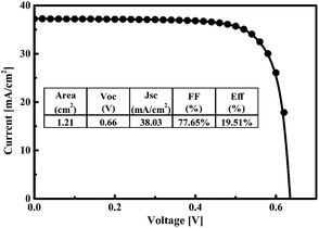
In this work, we have shown the PVSK/SHJ tandem cell preparation process and efficiency improvement pathway on the commercialized silicon substrate. The key point of the top cell band gap and CsBr–PbI2 precursor reactivity in the PVSK/SHJ tandem cells were solved by simple composition engineering. We successfully prepared monolithic two-terminal PVSK/SHJ tandem cells with a PCE of 23.22% by stacking the perovskite top cells on the double-side textured SHJ bottom cells with PCE of 19.51%. The sequential thermal evaporation/spin-coating processes had been utilized to achieve the conformal deposition of the perovskite layers. The composition of the perovskite absorber was carefully tuned by introducing CsBr during the PbI2 precursor layer evaporation in which the composition was adjusted via alternating the co-evaporating rates of the two powder sources. The concentrations of FAI/FABr solutions were varied to verify the current matching in the tandem solar cells. The influence of variation in composition on the band gap, defects, morphology, and resulting current match and device characteristics in the PVSK/SHJ tandem cells was investigated systematically. Not only a simple method for fabrication and modification of superior perovskite absorber but also a gained insights and correlations between composition and device performance including current matching, carrier collection, and defects passivation are addressed, which eventually gives rise to guidance towards high-performance monolithic PVSK/SHJ tandem solar cells.
2. Results and discussions
2.1 Structure of the PVSK/SHJ tandem solar cells
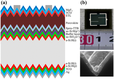
A commercial double-side textured n-type silicon (156.75 × 156.75 mm2) wafer with a thickness of 180 μm was employed for the SHJ bottom cell. The silicon wafer treated with standard texturing and RCA cleaning process14 was loaded in plasma enhanced chemical vapor deposition (PECVD) system to deposit the passivation layers of hydrogenated intrinsic amorphous (i-a-Si:H) stacks on both sides. Then, n-type μc-SiOx:H and p-type a-Si:H films were deposited on the front and back side respectively in the same system as the carrier selective layers.31 A bilayer junction of heavily doped and subsequent lightly doped p-type μc-Si:H film was deposited on the n-type μc-SiOx:H film to realize the carriers' tunneling. The SHJ bottom cell was completed by sputtering ITO film on the rear side in a magnetron sputtering system. Finally, the bottom cell was cut into a square shape with an area of 20.5 × 20.5 mm2 as the substrate for the top cell preparation. The perovskite top cell with p-i-n configuration was fabricated on the tunnel junction as following steps: evaporation of the hole transport material, conformal deposition of CsxFA1−xPbI3−yBry perovskite film by evaporation/spin-coating process, evaporation of the electron transport material. The active area of 1.2 cm2 was defined by deducting the metal frame shadow. A schematic diagram and real view of the monolithic two terminal PVSK/SHJ tandem cells were shown in Fig. 1.2.2 Band gap tuning of the PVSK absorber
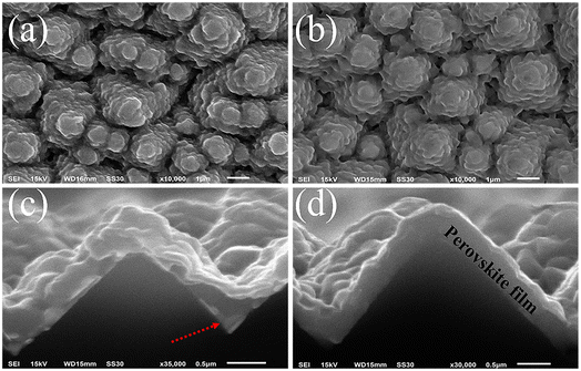
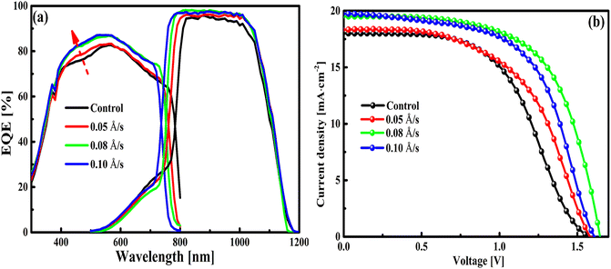
To better understand the influence of CsBr incorporation on the perovskite film performance, the morphology of PbI2 precursor layers with/without CsBr was studied by scanning electron microscope (SEM). Detailed information about CsBr's influence on perovskite morphology was investigated after spin-coating the FAI/FABr solution on the textured precursor layers. The perovskite film formed from pure PbI2 precursor showed a poor film of many ravines and scarce domain connections while smooth perovskite film with evenly sized and well-connected domains presented from the CsBr/PbI2 precursor (Fig. 2a and b). As seen from the cross-section images (Fig. 2c and d), a discontinuous film with cluttered perovskite crystals was formed from pure PbI2 precursor, while conformal and continuous film formed and spread over the pyramid texture by CsBr incorporation. Additionally, residual PbI2 (ref. 32) evidenced as white spots (red arrow marked) at the interface between perovskite and HTL was greatly reduced in the presence of CsBr. That is because the incorporation of Cs+ cations can loosen the microstructure of the precursor and accelerate diffusion and reaction of the FAI/FABr solution to form high-quality perovskite films. Namely, thermal-evaporated PbI2/CsBr layers may form the perovskite frame with loosen microstructure, and this porous layer was favorable for the FAI/FABr salts to diffuse and react with the PbI2 precursor layer.33According to the working principle of 2T tandem solar cells, the current of the top and bottom cells should be matched to ensure smooth carrier collection and transport, which is directly related to the JSC and FF of the tandem solar cells. As the performance and process conditions of the bottom SHJ solar cells are quite substantial and established in our research,16,34 we systematically investigated the device performance dependency on the band gap of the perovskite absorber layer, specifically determined by the ratio and deposition rate of CsBr incorporation. The optical response behavior of the tandem cells was evaluated by EQE. The band gap of the perovskite films was increased by increasing the CsBr content as evidenced by the blue-shifted absorption edge in Fig. 3a. Moreover, the incorporation of CsBr significantly enhanced the optical response of the top cells. This phenomenon can be explained by superior perovskite film with a smooth surface and regular grains, which was owing to the higher reaction extent of the FAI/FABr solution in loosened film of the CsBr/PbI2 precursor. That is, trap state density reduced by Cs+ cation enables longer carrier lifetime and enhanced collection for photo-generation carriers.35 The band gap of perovskite films calculated from the absorption edge and current density for the sub-cells were listed in Table 1. As the deposition rate of CsBr increased when co-evaporating with PbI2, coupling with the increased ratio of CsBr in the perovskite absorber, the current density of the top cell decreased while that of the bottom cell increased till they were best matched (Mismatch factor of 1.60%; mismatch factor = |JTop − JBottom|/JTotal) at the rate of 0.08 Å s−1. This is because when the perovskite top cell with a wider band gap, the bottom SHJ cell will receive more photons around 800 nm and generate a higher current till matched with the top cell current. As shown in Fig. 3(b) the S shape in the J–V curve of the control device was relieved as CsBr incorporated and eliminated at the rate of 0.08 Å s−1. It is well known that the S shape in J–V curves indicates that the majority of carriers accumulate36 at the interface due to poor transport ability in carrier selective layers or energy barrier between perovskite and carriers selective layers. Therefore, the incorporation of CsBr greatly suppressed carrier accumulation at the interface and induced a favorable energy alignment.
| Condition | Top [mA cm−2] | Bottom [mA cm−2] | Total [mA cm−2] | Mismatch factor (%) | Band gap [eV] |
|---|---|---|---|---|---|
| Control | 19.64 | 18.41 | 38.06 | 3.23 | 1.55 |
| 0.05 Å s−1 | 19.00 | 19.73 | 38.73 | 1.88 | 1.57 |
| 0.08 Å s−1 | 19.47 | 20.10 | 39.47 | 1.60 | 1.60 |
| 0.10 Å s−1 | 18.76 | 21.19 | 39.96 | 6.21 | 1.63 |
The change of the photovoltaic parameters of the PVSK/SHJ tandem cells with a deposition rate of CsBr was shown in Table 2. VOC, JSC, and FF as well as PCE of the tandem devices were continuously improved when the deposition rate of CsBr was increased from the control device to 0.05 and 0.08 Å s−1. This is consistent with the above EQE results that a wider band gap of the perovskite absorber layer induced by CsBr incorporation would increase the VOC of the tandem device and generate a better-matched current between the top and bottom cells, which is favorable for a higher FF. On the other hand, trap state density related to grain boundaries, excess PbI2, and ion vacancies can be largely suppressed by the introduction of Cs+ cations, and thus the VOC loss can be further minimized.35 It also observed that the current density of the whole device was maintained at a high level when further increasing in deposition rate to 0.10 Å s−1. However, the mismatched current between the sub-cells, as elucidated in the EQE study, would cause carriers accumulation at the interface and lead to low FF, which is the major reason responsible for the drop in the conversion efficiency. As a result, the highest efficiency was obtained from the perovskite absorber layer with a CsBr deposition rate of 0.08 Å s−1, which has a band gap of 1.6 eV.
| Condition | JSC [mA cm−2] | VOC [V] | FF [%] | PCE [%] |
|---|---|---|---|---|
| Control | 18.00 | 1.57 | 53.47 | 15.10 |
| 0.05 Å s−1 | 18.33 | 1.58 | 54.57 | 15.82 |
| 0.08 Å s−1 | 19.27 | 1.68 | 67.16 | 21.67 |
| 0.10 Å s−1 | 19.10 | 1.63 | 52.19 | 16.27 |
2.3 Grain growth for PVSK/SHJ tandem cells
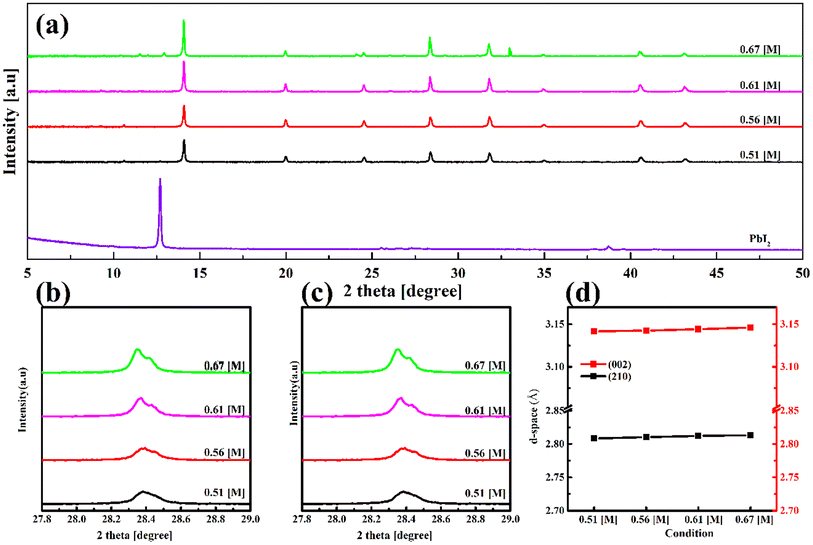
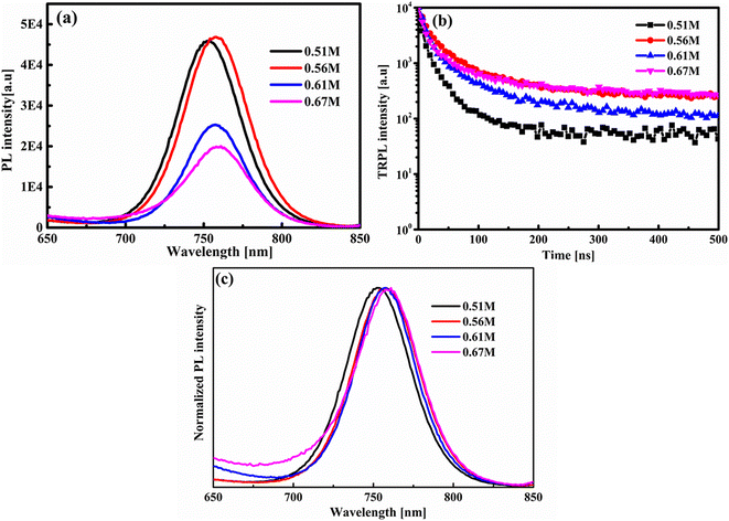
Based on the previous morphology result and initial device photovoltaic parameter, we found that grain morphology and current match tremendously affected the performance of the PVSK/SHJ tandem solar cells. To keep a well-matched current for the tandem cells, a CsBr evaporation rate of 0.08 Å s−1 was chosen in the subsequent investigation. FAI/FABr solutions of varying concentrations in ethyl alcohol were spin-coated onto the CsBr/PbI2 precursor film on a glass substrate and then the wet films were annealed at 170 °C for 30 minutes. The formed perovskite films were characterized by XRD. As shown in Fig. 4(a), the diffraction peak at 12.7° disappeared in the XRD pattern, indicating that PbI2 had been successfully translated to the perovskite phase. This neat reaction again demonstrated that cation or anion in FAI/FABr solution could easily diffuse into the porous CsBr/PbI2 precursor films. Accordingly, the diffraction peak belonging to the orientation of (001) for the CsxFA1−xPbI3−yBry phase was found at 14.05°. Meanwhile, diffraction peaks became much sharper when the concentration of the organic solution increased from 0.51 M to 0.67 M. Furthermore, both the orientations of (002) and (102) peaks in perovskite phases shifted to a low angle when the solution concentration increased, as shown in Fig. 4(b) and (c). The d-spacing calibrated according to Brag's law was slightly increased with adding concentration (Fig. 4(d)), attributing to crystal lattice expansion as more FA+ cations were filled into the crystal lattice.35,37Time-resolved photoluminescence (TR-PL) spectrum was measured to monitor the effect of FAI/FABr solution concentration on the carrier extraction ability in perovskite films. The semi-finished cell (without ETL and followed layers) prepared by various FAI/FABr solution concentrations on the textured bottom cells were used for measurement. As displayed in Fig. 5, the steady-state photoluminescence (PL) intensity slightly degraded with solution concentration decreasing from 0.51 M to 0.61 M, while dramatically dropping at 0.67 M. This quenching effect of the PL intensity peak indicated that non-radiative recombination in the perovskite layer had been increased.38 The minority carrier lifetime of the semi-finished tandem cells was acquired by fitting the TR-PL decay data with a tri-exponential decay model:39 Y = A1![[thin space (1/6-em)]](https://www.rsc.org/images/entities/char_2009.gif) exp(−t/τ1) + A2
exp(−t/τ1) + A2![[thin space (1/6-em)]](https://www.rsc.org/images/entities/char_2009.gif) exp(−t/τ2) + A2
exp(−t/τ2) + A2![[thin space (1/6-em)]](https://www.rsc.org/images/entities/char_2009.gif) exp(−t/τ3) + Bkgrdec, where τ1/τ2 and τ3 are ascribed to the recombination, the τav = (A1τ1 + A2τ2 + A3τ3)/(A1 + A2 + A3) was used to evaluate lifetimes. The estimated lifetime of 239 ns with 0.56 M solution concentration was attributed to mitigate defects in the compact absorber with appropriate residual PbI2,33 which would be studied carefully in the next section. However, further increases in FAI/FABr solution concentration led to a diminished lifetime of 97 ns, as listed in Table 3, which was likely caused by the recombination center located at the pinholes at the grain boundaries and interface, as suggested by the SEM images (Fig. 6). Moreover, a slightly red-shift emission peak in the normalized PL spectrum (Fig. 5(c)) suggested that the band gap was slightly narrowed by incorporating more FA+ cations.40
exp(−t/τ3) + Bkgrdec, where τ1/τ2 and τ3 are ascribed to the recombination, the τav = (A1τ1 + A2τ2 + A3τ3)/(A1 + A2 + A3) was used to evaluate lifetimes. The estimated lifetime of 239 ns with 0.56 M solution concentration was attributed to mitigate defects in the compact absorber with appropriate residual PbI2,33 which would be studied carefully in the next section. However, further increases in FAI/FABr solution concentration led to a diminished lifetime of 97 ns, as listed in Table 3, which was likely caused by the recombination center located at the pinholes at the grain boundaries and interface, as suggested by the SEM images (Fig. 6). Moreover, a slightly red-shift emission peak in the normalized PL spectrum (Fig. 5(c)) suggested that the band gap was slightly narrowed by incorporating more FA+ cations.40
| Condition | τav [ns] |
|---|---|
| 0.51 M | 124.6 |
| 0.56 M | 239.0 |
| 0.61 M | 127.0 |
| 0.67 M | 97.0 |
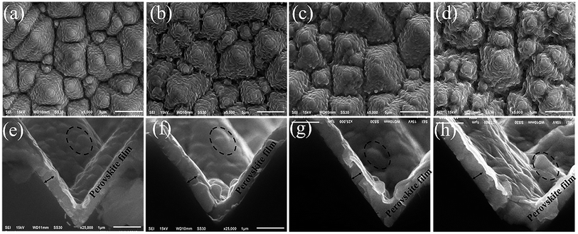 | ||
| Fig. 6 Surface (a–d) and cross-section (e–h) SEM images of the complete PVSK/SHJ tandem solar cells with solution concentrations of 0.51 M, 0.56 M, 0.61 M, and 0.67 M, respectively. | ||
To further reveal the grain growth behavior of perovskite with various solution concentrations, top-view and cross-section SEM results of the different perovskite films are displayed in Fig. 6. The surface morphology in Fig. 6(a)–(d) showed that uniform and conformal perovskite layers were successfully grown on the pyramid surface. From the cross-section images, visible enlargement in grain size for the perovskite film with higher concentrations was found as marked in the black imaginary line region in Fig. 6(e)–(h). It is consistent with XRD results that diffraction peaks become sharper at higher solution concentrations, implying large average grain size. The perovskite film formed at low concentration is more compact while the surface roughness is gradually increased with a bigger grain size. On the other hand, white spots and small crystal grains (red imaginary line region) in Fig. 6(e) were found at the interface between the silicon bottom cell and perovskite film when using 0.51 M solution concentration. These spots were associated with residual lead iodide which was not reacted32,41 with FAI/FABr solutions as mentioned in the previous section. The white spots disappeared when increasing the solution concentration to 0.67 M. According to the SEM images, it was also found that the thickness of the perovskite film increased by 30 nm when the FAI/FABr concentration increased from 0.51 M to 0.67 M. Complete reaction of PbI2 with FAI/FABr fully produced grown grains and thicker perovskite absorber. While the improved grain size brought several bad effects, which is detail discussed in the next section.
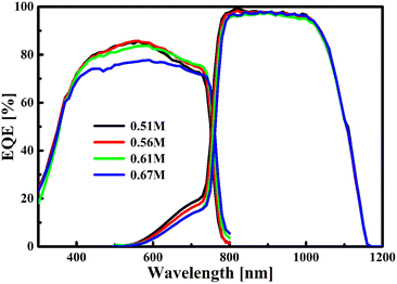
To evaluate the photovoltaic parameters of PVSK/SHJ tandem cells affected by grain growth, complete tandem cells were fabricated with sequential depositions including hole transport layer, CsBr/PbI2 evaporation, solution spin coating, electron transport layer and transport conduct oxide film (as Fig. 1a). The spectrum response collected by the EQE measurement system was displayed in Fig. 7. For the top cell, a slight red shift of the absorption edge was found by increasing solution concentration. This shift indicates that a FAPbIxBr3−x absorber of lower band gap (1.5 eV) was formed after spin-coating with a higher concentration of FAI/FABr solution.40 Another significant finding was that the spectrum response of the top cell was enhanced at a wavelength of 600–700 nm mainly benefiting from narrowed band gap and additional film thickness. However, further increments in grain size and thickness by raising solution concentration yielded a rough surface morphology of irregular and smaller pyramids with poor light-trapping effect.42 The poor surface morphology also accelerated the non-radiation recombination in the film which should be responsible for the reduced photocurrent of the tandem devices from solution concentrations of 0.61 M and 0.67 M, as shown in the EQE curves and Table 4. Eventually, the tandem device from 0.56 M demonstrated the best combination of total current density (39.08 mA cm−2) and fairly matched sub-cell current density (19.38 mA cm−2 and 19.71 mA cm−2 for the top and bottom cells, respectively).
| Concentration | Top [mA cm−2] | Bottom [mA cm−2] | Total [mA cm−2] | Mismatch factor (%) |
|---|---|---|---|---|
| 0.51 M | 19.07 | 20.08 | 39.16 | 2.58 |
| 0.56 M | 19.38 | 19.71 | 39.08 | 0.84 |
| 0.61 M | 19.40 | 19.12 | 38.51 | 0.73 |
| 0.67 M | 18.50 | 19.04 | 37.54 | 1.44 |
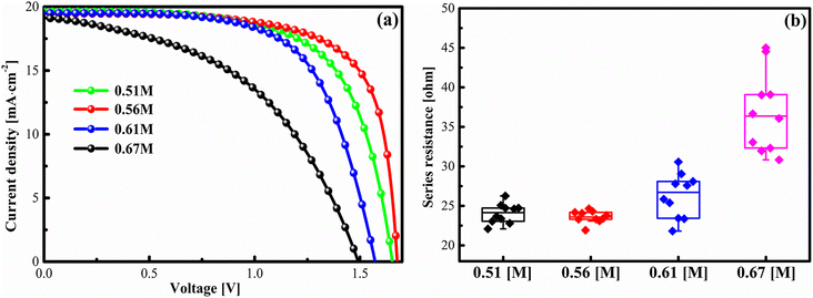
The J–V characteristics of each cell were recorded by an IV tester system under AM1.5 illumination while stacked with an optical mask. J–V parameters were measured from the reverse scan with a voltage sweeping step at 100 mV, as shown in Fig. 8. JSC showed a continuous drop as solution concentration increased, due to lowering spectrum response as evidenced by the EQE curves. VOC reached the maximum value of 1.71 V for devices at 0.56 M, likely due to good passivation of the defects at the interface and grain boundaries enabled by optimal residual PbI2.37 However, the VOC sharply decreased at higher solution concentrations (0.61 M and 0.67 M) due to more defects, recombination centers coming from the unexcepted surface morphology of perovskite film, and the band gap narrowed. Interestingly, the tandem devices from the 0.56 M solution presented about 0.05 promotion in average fill factor compared to that of the 0.51 M batches, which was considered as the major contribution to the maximum PCE of the 0.56 M batches. This promotion was attributed to a well matched current density between sub-cells and less residual PbI2 grains at the interface which can act as a resist layer for the carriers (holes in this work) transport.43 Series resistance calibrated from the J–V curves(Fig. 9(a)) suggested a much higher value in the case of the high concentration 0.61 M and 0.67 M (Fig. 9(b)) owing to current mismatch and noticeable pinholes as shown in Fig. 6(e–h) (black imaginary line region). Based on the above study, concluded that the quantity of the residue PbI2 needs to be controlled at an optimal level. Specifically, reasonable residue PbI2 can act as a good defect passivation species while too much residue PbI2 could lead to high series resistance,43,44 as the former is beneficial to carrier lifetime as well as VOC while the latter is unfavorable to charge collection and resulting FF degradation. As such, tuning the concentration of the FAI/FABr solution is an efficient method of controlling the residue level of PbI2 as well as an optimized grain growth and film morphology. Eventually, a champion device out of the 0.56 M batches presented the best conversion efficiency of 23.22% with VOC of 1.68 V, JSC of 19.47 mA cm−2, and FF of 0.71.
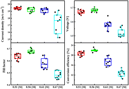 | ||
| Fig. 8 J–V Characteristics of the PVK/SHJ solar cells from different solution concentrations (each group contains 10 cells). | ||
3. Conclusions
In summary, we have shown a two-step preparation process of PVSK/SHJ tandem cell on the double-side textured silicon substrate, which is the most promising commercialized route. The two-step processing method of evaporated PbI2 layer and organic salt solution spin-coat assures perovskite absorber conformal deposition on the rough pyramid textures. The composition engineering is developed to optimize the current match of the sub-cells and diminish the defects of the 2T tandem solar cells based on a textured crystal silicon substrate. The results show that introducing CsBr at varied co-evaporating rates has optimized the current match of the sub-cells because of band gap tuning, and various concentrations of FAI/FABr solutions have diminished the defects owing to the perovskite grain growth. As the deposition rate of CsBr increased, the current density of the top cell decreased while that of the bottom cell increased till they were best matched at the rate of 0.08 Å s−1. Furthermore, tuning the concentration of the FAI/FABr solution is an efficient method of controlling the residue level of PbI2 as well as an optimized grain growth and film morphology. Specifically, certain residue PbI2 acted as good defect passivation species while too much residue PbI2 led to high series resistance, which turned out to be a trade-off tuning between VOC and FF. Eventually, a champion device out of the 0.56 M batches presented the best conversion efficiency of 23.22% with VOC of 1.68 V, JSC of 19.47 mA cm−2, and FF of 0.71. This study not only highlighted a simple method for fabrication and optimization of perovskite absorber but also gained insights and guidelines for high-performance monolithic PVSK/SHJ tandem solar cells in terms of the superior current match, carrier collection, and transport.4. Experimental section
4.1 SHJ bottom cell preparation
A M2 n-type Cz wafers with a resistivity of 1–3 Ω and a thickness of 180 μm were used as a silicon substrate. Silicon wafers first suffered standard textured and RCA clean process. After that, intrinsic and boron-doped hydrogenated amorphous silicon layers were deposited on the rear side in a very high-frequency plasma-enhanced chemical vapor deposition (VHF-PECVD) system for dangling bond passivation and hole selection.45–47 And then, intrinsic and phosphorus-doped micro-crystal silicon oxide film (n-a-SiOx:H) were deposited on the front side using the same system. As for tandem cells, tunnel junction plays an important role in carriers transporting between sub-cells. In the work, the tunnel junction was finished by sequential stacking heavily and light boron-doped microcrystal silicon (p-a-Si:H) on the n-a-SiOx:H. Additionally, 110 nm indium tin oxide (ITO, 90% In2O3 and 10% SnO2, sheet resistance of 85 Ω sq−1 measured by a four-point probe Hall measurement system) film was sputtered on the p-a-Si:H in the magnetron sputter system and formed the back electrode.48 Finally, the SHJ cells with tunnel junction were cut into square shapes at an area of 20.5 × 20.5 mm2 by laser to handle the following stacks processes. The J–V curve and parameters of the bottom cell was displayed in Fig. 10.4.2 Perovskite top cell preparation
Perovskite solar cells were fabricated with p-i-n configuration by stacking function layers on the tunnel junction. Firstly, 10 nm 2,2′,7,7′-tetra(N,N-di-tolyl)amino-9,9-spiro-bifluorene (spiro-TTB, >99%, Lumtec) was thermally evaporated (evaporation rate of 0.15 Å s−1 as measured by a crystal monitor) on the tunnel junction act as the hole-selection layer. Then, PbI2 (>99.99%, purchased from TCI) and CsBr (>99.9%, Baolai, Xi'an) were co-evaporated at the same vacuum system, the composition was tuned by adjusting the evaporate rates. Subsequently, a mixture solution of FAI (≥99.5%, purchased from Xi'an Polymer Light Technology) and FABr (molar ratio of 3 to 1 dissolved in ethanol, Sigma-Aldrich) was spin-coated on the PbI2–CsBr precursor layer, and the solution concentration used in this work listed in Table 5. The solution process used a dynamic spin with rotation speed of 4000 rpm and accelerated velocity of 2000 rpm within 30 seconds while the ambient humidity was under 4%. The perovskite films finished crystallization on a hot plate at 170 °C for 30 minutes while the ambient humidity was maintained at 50–70%. After that, 1 nm of LiF (>99.98%, Sigma-Aldrich) and 10 nm electron-selection layer C60 (>99%, Xi'an Polymer Light Technology) were thermally evaporated by a home-made evaporation system (evaporation rate of 0.06 Å s−1 for LiF and of 0.15 Å s−1 for C60). A buffer layer of SnO2 of 160 cycles was deposited in atomic layer deposition at 85 °C using tetrakis (dimethylamino) tin and H2O as precursors. The indium tin oxide (ITO) of 110 nm (sheet resistance of 90 Ω sq−1) was sputtered. Ag electrode was thermally evaporated on the front and back sides using a shadow mask. Finally, antireflective films of MgF2 (100 nm, >99.99%, Sigma-Aldrich) were deposited on the front surface in the electron beam evaporation system. The attention that the deposition rate must be stabilized at the target rate before layer depositing. The active area of 1.2 cm2 was defined by deducting the metal frame shadow.| FAI [mg] | FABr [mg] | Solvent [ml] | Total concentration [M] |
|---|---|---|---|
| 66.0 | 16.0 | 1 | 0.51 |
| 72.6 | 17.6 | 1 | 0.56 |
| 79.2 | 19.2 | 1 | 0.61 |
| 85.8 | 20.8 | 1 | 0.67 |
4.3 Characterizations
XRD diffraction pattern was recorded by Empyrean (D8 Advance, Bruker) with Cu K-alpha radiation (λ = 0.15406 nm) with a scan step size of 0.03°. Morphology was assessed by a scanning electron microscope (Jsm-6510; JEOL Ltd., Japan). The time-resolved photoluminescence (TR-PL) of perovskite films was characterized by the Edinburgh Instruments FLS 980 fluorescence spectrometer. The performance parameters were measured under AM 1.5 G (1000 W m−2) using 1000 W xenon as the light source (VS-0851A; Yamashita Denso Co., Ltd, Japan), while a Keithley-2460 source meter was used for data collection. The light intensity was calibrated using an AvaSolar simulator system (Fluotime 300, picoquant). The J–V curve was performed from 1.8 V to −0.1 V at step −0.02 V for each point. EQE spectrum response for sub-cells was recorded on an EQE system (QE-R, Enli Technology Co., Ltd.), and the wavelength range of 300–800 nm & 500–1200 nm for top and bottom cells respectively. Similarly, the excitation light intensity is calibrated by a Si photodiode. A square shape mask with an area of 1.21 cm2 was used during the J–V measurement.Conflicts of interest
Authors have no financial/commercial Conflict of Interest.Acknowledgements
This project is supported by the National Science Foundation of China (NSFC No. 11574014), the General Projects of Shenzhen Stable Development (grant number: SZWD2021004), and Shenzhen Key Laboratory of Marine Energies and Environmental Safety (grant number: ZDSYS20201215154000001). The authors also appreciate Dr Yuan-min Li for his great support and assistance in experimental designing and performance improvement. Furthermore, the authors are also grateful to Dr Minghao Qu, Dr Xin Dong, Dr Hongfeng Lin, Dr Wei Long, Xiaobing Gu, Lan Chen, Wenchao Wei, Yanfen Wang at Hanergy Thin Film Solar Group, R & D Center, for the great support and helpful discussions in this work.References
- K. Yoshikawa, W. Yoshida, T. Irie, H. Kawasaki, K. Konishi, H. Ishibashi, T. Asatani, D. Adachi, M. Kanematsu, H. Uzu and K. Yamamoto, Exceeding conversion efficiency of 26% by heterojunction interdigitated back contact solar cell with thin film Si technology, Sol. Energy Mater. Sol. Cells, 2017, 173, 37–42 CrossRef CAS
.
- K. Yoshikawa, H. Kawasaki, W. Yoshida, T. Irie, K. Konishi, K. Nakano, T. Uto, D. Adachi, M. Kanematsu, H. Uzu and K. Yamamoto, Silicon heterojunction solar cell with interdigitated back contacts for a photoconversion efficiency over 26%, Nat. Energy, 2017, 2(5), 17032 CrossRef CAS
.
- T. P. White, N. N. Lal and K. R. Catchpole, Tandem Solar Cells Based on High-Efficiency c-Si Bottom Cells: Top Cell Requirements for >30% Efficiency, IEEE J. Photovolt., 2014, 4(1), 208–214 Search PubMed
.
- W. E. I. Sha, X. D. Ren, L. Z. Chen and W. C. H. Choy, The efficiency limit of CH3NH3PbI3 perovskite solar cells, Appl. Phys. Lett., 2015, 106(12), 221104 CrossRef
.
- J. Li, E. Alvianto and Y. Hou, Developing the Next-Generation Perovskite/Si Tandems: Toward Efficient, Stable, and Commercially Viable Photovoltaics, ACS Appl. Mater. Interfaces, 2022, 14(30), 34262–34268 CrossRef CAS PubMed
.
- F. Khan, B. D. Rezgui, M. T. Khan and F. Al-Sulaiman, Perovskite-based tandem solar cells: Device architecture, stability, and economic perspectives, Renewable Sustainable Energy Rev., 2022, 165, 112553 CrossRef CAS
.
- I. Almansouri, A. Ho-Baillie and M. A. Green, Ultimate efficiency limit of single-junction perovskite and dual-junction perovskite/silicon two-terminal devices, Jpn. J. Appl. Phys., 2015, 54(8S1), 08KD04 CrossRef
.
- A. Kojima, K. Teshima, Y. Shirai and T. Miyasaka, Organometal halide perovskites as visible-light sensitizers for photovoltaic cells, J. Am. Chem. Soc., 2009, 131(17), 6050–6051 CrossRef CAS PubMed
.
- M. Kim, J. Jeong, H. Lu, T. K. Lee, F. T. Eickemeyer, Y. Liu, I.-w. Choi, S. J. Choi, Y. Jo, H.-B. Kim, S.-I. Mo, Y.-K. Kim, H. Lee, N. G. An, S. Cho, W. R. Tress, S. M. Zakeeruddin, A. Hagfeldt, J. Y. Kim, M. Gratzel and D. S. Kim, Conformal quantum dot-SnO2 layers as electron transporters for efficient perovskite solar cells, Science, 2022, 375(6578), 302–306 CrossRef CAS PubMed
.
- A. Kojima, K. Teshima, Y. Shirai and T. Miyasaka, Organometal halide perovskites as visible-light sensitizers for photovoltaic cells, J. Am. Chem. Soc., 2009, 131(17), 6050–6051 CrossRef CAS PubMed
.
- P. Wang, Y. Wu, B. Cai, Q. Ma, X. Zheng and W. H. Zhang, Solution-Processable Perovskite Solar Cells toward Commercialization: Progress and Challenges, Adv. Funct. Mater., 2019, 29(47), 1087661 Search PubMed
.
- X. Dai, Y. Deng, C. H. Van Brackle, S. Chen, P. N. Rudd, X. Xiao, Y. Lin, B. Chen and J. Huang, Scalable Fabrication of Efficient Perovskite Solar Modules on Flexible Glass Substrates, Adv. Energy Mater., 2019, 10(1), 1903108 CrossRef
.
- M. Agarwal, A. Pawar, N. Wadibhasme and R. Dusane, Controlling the c-Si/a-Si:H interface in silicon heterojunction solar cells fabricated by HWCVD, Sol. Energy, 2017, 144, 417–423 CrossRef CAS
.
- S. De Wolf, A. Descoeudres, Z. C. Holman and C. Ballif, High-efficiency Silicon Heterojunction Solar Cells: A Review, Green, 2012, 2(1), 7–24 CrossRef CAS
.
- D. Adachi, J. L. Hernández and K. Yamamoto, Impact of carrier recombination on fill factor for large area heterojunction crystalline silicon solar cell with 25.1% efficiency, Appl. Phys. Lett., 2015, 107(23), 233506 CrossRef
.
- Y. Cao, Y. Miao and D. Gangqiang, Development of silicon heterojunction solar cell technology for manufacturing, Jpn. J. Appl. Phys., 2018, 57, 08RB15 CrossRef
.
- F. Sahli, J. Werner, B. A. Kamino, M. Brauninger, R. Monnard, B. Paviet-Salomon, L. Barraud, L. Ding, J. J. Diaz Leon, D. Sacchetto, G. Cattaneo, M. Despeisse, M. Boccard, S. Nicolay, Q. Jeangros, B. Niesen and C. Ballif, Fully textured monolithic perovskite/silicon tandem solar cells with 25.2% power conversion efficiency, Nat. Mater., 2018, 17(9), 820–826 CrossRef CAS PubMed
.
- Z. Yu, M. Leilaeioun and Z. Holman, Selecting tandem partners for silicon solar cells, Nat. Energy, 2016, 1(11), 16137 CrossRef
.
- NREL, Best-research-cell-efficiencies, 2022. https://www.nrel.gov/pv/cell-efficiency.html Search PubMed
.
- G. Nogay, F. Sahli, J. Werner, R. Monnard, M. Boccard, M. Despeisse, F. J. Haug, Q. Jeangros, A. Ingenito and C. Ballif, 25.1%-Efficient Monolithic Perovskite/Silicon Tandem Solar Cell Based on a p-type Monocrystalline Textured Silicon Wafer and High-Temperature Passivating Contacts, ACS Energy Lett., 2019, 4(4), 844–845 CrossRef CAS
.
- O. S. T. Shen H and D. A. Jacobs, et al., In situ recombination junction between p-Si and TiO2 enables high-efficiency monolithic perovskite/Si tandem cells, Sci. Adv., 2018, 4(12), eaau9711 CrossRef
.
- S. Mariotti, K. Jäger, M. Diederich, M. S. Härtel, B. Li, K. Sveinbjörnsson, S. Kajari-Schröder, R. Peibst, S. Albrecht, L. Korte and T. Wietler, Monolithic Perovskite/Silicon Tandem Solar Cells Fabricated Using Industrial p-Type Polycrystalline Silicon on Oxide/Passivated Emitter and Rear Cell Silicon Bottom Cell Technology, Sol. RRL, 2022, 6(4), 2101066 CrossRef CAS
.
- K. A. Bush, A. F. Palmstrom, Z. J. Yu, M. Boccard, R. Cheacharoen, J. P. Mailoa, D. P. McMeekin, R. L. Z. Hoye, C. D. Bailie, T. Leijtens, I. M. Peters, M. C. Minichetti, N. Rolston, R. Prasanna, S. Sofia, D. Harwood, W. Ma, F. Moghadam, H. J. Snaith, T. Buonassisi, Z. C. Holman, S. F. Bent and M. D. McGehee, 23.6%-efficient monolithic perovskite/silicon tandem solar cells with improved stability, Nat. Energy, 2017, 2(4), 17009 CrossRef CAS
.
- J. Zheng, C. F. J. Lau, H. Mehrvarz, F.-J. Ma, Y. Jiang, X. Deng, A. Soeriyadi, J. Kim, M. Zhang, L. Hu, X. Cui, D. S. Lee, J. Bing, Y. Cho, C. Chen, M. A. Green, S. Huang and A. W. Y. Ho-Baillie, Large area efficient interface layer free monolithic perovskite/homo-junction-silicon tandem solar cell with over 20% efficiency, Energy Environ. Sci., 2018, 11(9), 2432–2443 RSC
.
- F. Sahli, B. A. Kamino, J. Werner, M. Bräuninger, B. Paviet-Salomon, L. Barraud, R. Monnard, J. P. Seif, A. Tomasi, Q. Jeangros, A. Hessler-Wyser, S. De Wolf, M. Despeisse, S. Nicolay, B. Niesen and C. Ballif, Improved Optics in Monolithic Perovskite/Silicon Tandem Solar Cells with a Nanocrystalline Silicon Recombination Junction, Adv. Energy Mater., 2018, 8(6), 1701609 CrossRef
.
- Y. Wang, C. Gao, X. Wang, H. Liu and W. Shen, Controllable Electrochemical Deposition and Theoretical Understanding of Conformal Perovskite on Textured Silicon towards Efficient Perovskite/Silicon Tandem Solar Cells, J. Phys. Chem. C, 2021, 125(5), 2875–2883 CrossRef CAS
.
- A. Ho-Baillie, Perovskites cover silicon textures, Nat. Mater., 2018, 17(9), 751–752 CrossRef CAS PubMed
.
- B. Chen, Z. J. Yu, S. Manzoor, S. Wang, W. Weigand, Z. Yu, G. Yang, Z. Ni, X. Dai, Z. C. Holman and J. Huang, Blade-Coated Perovskites on Textured Silicon for 26%-Efficient Monolithic Perovskite/Silicon Tandem Solar Cells, Joule, 2020, 4(4), 850–864 CrossRef CAS
.
- E. Aydin, T. G. Allen, M. De Bastiani, L. Xu, J. Ávila, M. Salvador, E. Van Kerschaver and S. De Wolf, Interplay between temperature and bandgap energies on the outdoor performance of perovskite/silicon tandem solar cells, Nat. Energy, 2020, 5(11), 851–859 CrossRef CAS
.
- E. Köhnen, M. Jošt, A. B. Morales-Vilches, P. Tockhorn, A. Al-Ashouri, B. Macco, L. Kegelmann, L. Korte, B. Rech, R. Schlatmann, B. Stannowski and S. Albrecht, Highly efficient monolithic perovskite silicon tandem solar cells: analyzing the influence of current mismatch on device performance, Sustainable Energy Fuels, 2019, 3(8), 1995–2005 RSC
.
- M. Jošt, E. Köhnen, A. B. Morales-Vilches, B. Lipovšek, K. Jäger, B. Macco, A. Al-Ashouri, J. Krč, L. Korte, B. Rech, R. Schlatmann, M. Topič, B. Stannowski and S. Albrecht, Textured interfaces in monolithic perovskite/silicon tandem solar cells: advanced light management for improved efficiency and energy yield, Energy Environ. Sci., 2018, 11(12), 3511–3523 RSC
.
- Q. Jiang, Z. Chu, P. Wang, X. Yang, H. Liu, Y. Wang, Z. Yin, J. Wu, X. Zhang and J. You, Planar-Structure Perovskite Solar Cells with Efficiency beyond 21, Adv. Mater., 2017, 29(46), 1703852 CrossRef PubMed
.
- S. Rafizadeh, K. Wienands, P. S. C. Schulze, A. J. Bett, L. C. Andreani, M. Hermle, S. Glunz and J. C. Goldschmidt, Efficiency Enhancement and Hysteresis Mitigation by Manipulation of Grain Growth Conditions in Hybrid Evaporated-Spin-coated Perovskite Solar Cells, ACS Appl. Mater. Interfaces, 2019, 11(1), 722–729 CrossRef CAS PubMed
.
- X. Ru, M. Qu, J. Wang, T. Ruan, M. Yang, F. Peng, W. Long, K. Zheng, H. Yan and X. Xu, 25.11% efficiency silicon heterojunction solar cell with low deposition rate intrinsic amorphous silicon buffer layers, Sol. Energy Mater. Sol. Cells, 2020, 215, 110643 CrossRef CAS
.
- X. Zhu, D. Yang, R. Yang, B. Yang, Z. Yang, X. Ren, J. Zhang, J. Niu, J. Feng and S. F. Liu, Superior stability for perovskite solar cells with 20% efficiency using vacuum co-evaporation, Nanoscale, 2017, 9(34), 12316–12323 RSC
.
- E. T. Roe, K. E. Egelhofer and M. C. Lonergan, Exchange current density model for the contact-determined current-voltage behavior of solar cells, J. Appl. Phys., 2019, 125(22), 225302 CrossRef
.
- Y. Sun, J. Peng, Y. Chen, Y. Yao and Z. Liang, Triple-cation mixed-halide perovskites: towards efficient, annealing-free and air-stable solar cells enabled by Pb(SCN)2 additive, Sci. Rep., 2017, 7, 46193 CrossRef CAS
.
- Q. Jiang, L. Zhang, H. Wang, X. Yang, J. Meng, H. Liu, Z. Yin, J. Wu, X. Zhang and J. You, Enhanced electron extraction using SnO2 for high-efficiency planar-structure HC(NH2)2PbI3-based perovskite solar cells, Nat. Energy, 2016, 2(1), 16177 CrossRef
.
- H. Min, M. Kim, S. U. Lee, H. Kim, G. Kim, K. Choi, J. H. Lee and S. I. Seok, Efficient, stable solar cells by using inherent bandgap of alpha-phase formamidinium lead iodide, Science, 2019, 366(6466), 749–753 CrossRef CAS PubMed
.
- S. Tao, I. Schmidt, G. Brocks, J. Jiang, I. Tranca, K. Meerholz and S. Olthof, Absolute energy level positions in tin- and lead-based halide perovskites, Nat. Commun., 2019, 10(1), 2560 CrossRef PubMed
.
- J. Holovský, A. Peter Amalathas, L. Landová, B. Dzurňák, B. Conrad, M. Ledinský, Z. Hájková, O. Pop-Georgievski, J. Svoboda, T. C.-J. Yang and Q. Jeangros, Lead Halide Residue as a Source of Light-Induced Reversible Defects in Hybrid Perovskite Layers and Solar Cells, ACS Energy Lett., 2019, 4(12), 3011–3017 CrossRef
.
- S. Yang, P. Ge and L. Zhang, The effects of different parameters of pyramidal textured silicon surface on the optical reflectance, Sol. Energy, 2016, 134, 392–398 CrossRef CAS
.
- A. Liu, K. Liu, H. Zhou, H. Li, X. Qiu, Y. Yang and M. Liu, Solution evaporation processed high quality perovskite films, Sci. Bull., 2018, 63(23), 1591–1596 CrossRef CAS PubMed
.
- J. Euvrard, O. Gunawan and D. B. Mitzi, Impact of PbI2 Passivation and Grain Size Engineering in CH3NH3PbI3 Solar Absorbers as Revealed by Carrier-Resolved Photo-Hall Technique, Adv. Energy Mater., 2019, 9(47), 1902706 CrossRef CAS
.
- Y. Zhang, C. Yu, M. Yang, L.-R. Zhang, Y.-C. He, J.-Y. Zhang, X.-X. Xu, Y.-Z. Zhang, X.-M. Song and H. Yan, Significant Improvement of Passivation Performance by Two-Step Preparation of Amorphous Silicon Passivation Layers in Silicon Heterojunction Solar Cells, Chin. Phys. Lett., 2017, 34(3), 038101 CrossRef
.
- L. Oppong-Antwi, S. Huang, Q. Li, D. Chi, X. Meng and L. He, Influence of defect states and fixed charges located at the a-Si:H/c-Si interface on the performance of HIT solar cells, Sol. Energy, 2017, 141, 222–227 CrossRef CAS
.
- J. Schmidt, R. Peibst and R. Brendel, Surface passivation of crystalline silicon solar cells: Present and future, Sol. Energy Mater. Sol. Cells, 2018, 187, 39–54 CrossRef CAS
.
- M. Chen, Z. L. Pei, X. Wang, Y. Yu, X. Liu, C. Sun and L. S. Wen, Intrinsic limit of electrical properties of transparent conductive oxide films, J. Phys. D: Appl. Phys., 2000, 33(20), 2538–2548 CrossRef CAS
.
Footnote |
| † These authors contributed equally to this work. |
| This journal is © The Royal Society of Chemistry 2023 |

