 Open Access Article
Microstructure, grain and nanowire growth during selective laser melting of Ag–Cu/diamond composites†
Chenxing Xinab,
Xiya Zhaoab,
Haoze Gengab,
Liang Haoab,
Yan Li *ab,
Tao Chena and
Ping Gonga
aGemmological Institute, China University of Geosciences, Wuhan, 430074, P. R. China
bAdvanced Manufacturing Centre, China University of Geosciences, Wuhan, 430074, P. R. China. E-mail: yanli@cug.edu.cn
First published on 24th January 2023
Abstract
Selective laser melting (SLM) technique is a viable alternative to fabricating metal matrix composites (MMCs) with controllable structures; however, its implementation remains challenging because of the unpredicted defects arising from the reinforcement. This study primarily examined the microstructural evolution and grain growth in the Ag–Cu/diamond composites at the molten pool scale during the SLM process via a thermodynamic analysis. The feasibility of manufacturing Ag–Cu/diamond composites was verified using several processing parameters. Moreover, the influence of energy density on the microstructures and grain growth was also demonstrated theoretically and experimentally. The formation of different kinds of grain morphologies in the molten pool was ascribed to the temperature gradient and cooling rate, corresponding to the direction and size of grain growth. The generation of Ag–Cu nanowires at the grain boundaries was firstly found in the SLM technique, which was related to the pressure stress generated by the high cooling rate of SLM. This work hopefully opens new paths for the applications of high-performance Ag–Cu/diamond MMCs in various application fields. It also provides new possibilities for the controllable manufacturing of Ag nanowires during SLM.
Introduction
Metal matrix (pure metals and their alloys) composites (MMCs) are the most promising materials for advanced applications because of their high performance in terms of specific strength, thermal conductivity, rigidity, wear resistance and elastic modulus by adding fibres, whiskers and particles as reinforcing materials.1–4 Owing to the high thermal conductivity (up to 2000 W m−1 K−1), low thermal expansion coefficient (1.0 × 10⁻⁶ K−1), extremely high hardness, high wear resistance and chemical inertness of diamond, they are extensively used as a desirable reinforcement phase material in the Cu, Al, Ni and Ti metal matrix.5–8 Among the available metals, silver (Ag) alloy is regarded as an extremely favourable matrix because of its excellent electrical properties (1.59 × 10⁻⁸ Ω m), thermal conductivity (429 W m−1 K−1), high reflectivity (98.8%, 650 nm) and ductility (elongation: 25%min.).9,10 Hence, the Ag/diamond composite is an excellent combination of MMCs. The addition of nano/micron-sized diamond particles can customise Ag's coefficient of thermal expansion and enhance its corrosion resistance, mechanical properties, and thermal conductivity properties. This kind of MMCs is promising to revolutionise photodetections,11,12 thermal convection reuse,13 and imaging sensor industries.14To date, MMCs are primarily manufactured by solid-state processing (i.e. powder metallurgy, mechanical alloying) and liquid-state processing (i.e. squeeze casting, stir casting) methods.2 However, these methods can only produce simple geometries and substantially restrict the full capabilities of Ag-diamond composites. Selective laser melting (SLM), as a powder bed-based additive manufacturing technology, can fabricate sophisticated and precise structures via a laser beam to maximise the performance of materials by taking advantage of the structure design. Researchers have focussed on the diamond-reinforced Cu–Sn–Ti matrix, Al matrix15 and Cu matrix16 manufactured by SLM, and made some advancements with time. Tian et al.17 demonstrated the excellent compression, bending and flexural performance of the AlSi10Mg/diamond with cellular structures fabricated by SLM. Constantin et al.18 proposed the remelting strategy and realised a high thermal conductivity (349 W (m−1 K−1)) in the Cu/diamond composite. Gan et al.19 verified the better wear resistance of Cu–Sn–Ti/diamond manufactured by SLM compared to that of the hot-pressed sintered samples. However, the fabrication of MMCs by SLM is still in the preliminary stage, and the problems arising from the addition of diamond particles are still difficult to address. These issues significantly affect the densification behaviour of final parts. Although the feasibility of Ag–Cu alloy parts realised by SLM has been initially confirmed,9,20 the addition of diamond particles considerably alters the transit molten pool dynamics, rheology and flowability, resulting in unexpected defects.
Furthermore, a high-temperature gradient and a large cooling rate are generated in the molten pool because of the selective heating mechanism, which is linked to the formation of nuclei and grain growth. Importantly, the properties of SLM-processed parts are closely related to microstructural evolution and grain growth; for example, the anisotropism of columnar grains indicates the anisotropy of mechanical performance in the parts.21 Meanwhile, the boundary structure and misoriented grains in the molten pool may cause the performance deterioration of the final parts—the pores and cracks usually manifest in the microstructural transition area in the molten pool and the bonding region between the neighbouring molten pools.21,22 Due to the high thermal conductivity of diamonds, they can directly influence the heat transfer mechanism in the surrounding metal matrix, which also changes the thermal behaviour in the molten pool. Therefore, it is crucial to further examine the microstructural evolution and grain growth of SLM-fabricated parts at the molten pool scale through a comprehensive analysis of quantitative thermal behaviour and microstructural characterisation.
Here, the Ag–Cu/5 vol% diamond composites were successfully fabricated with an SLM printer by implementing different printing parameters (i.e. laser powder, scanning speed and hatch distance). Meanwhile, a three-dimensional (3D) numerical simulation of thermal behaviour within the molten pool of the Ag/diamond composites was performed during the SLM process. The Ag–Cu alloy nanowires were firstly observed in SLM 3D printing, and the origin of stress was also analysed. The microstructural development and matched grain growth mechanisms in the molten pools influenced the materials' characterisation but were less explored. Therefore, the optimisation of the parameters and the grain growth behaviour could open a new avenue for enhancing the properties of materials from the microstructural evolution. This study aims to investigate the internal relationship among thermal behaviour, microstructural evolution, and grain growth at the molten pool scale based on a comprehensive analysis of thermal dynamics and crystallography.
Experimental
Materials
Gas-atomised 92.5 wt% Ag alloy powders were supplied by the Legor Group Company, Italy. This Ag alloy, containing 7.5 wt% of other compositions, is also known as standard sterling silver and is widely used for commercial products and industrial components.20 According to the Legor Group Company report, the other 7.5 wt% of the reserved non-silver solute was mainly Cu. The diamond particles, coated with Ti, with a mean diameter of 25 μm, on the surface by a vacuum deposition method were provided by Henan Huajing Superhard Materials Co., Ltd. (China) (Fig. S1†).Preparation of Ag–Cu/diamond components via SLM
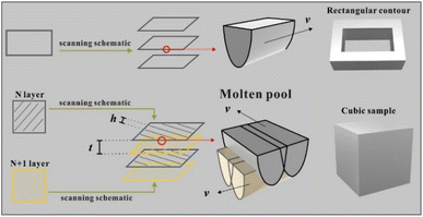
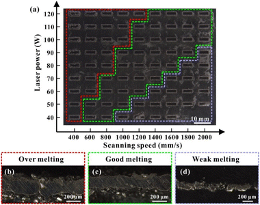
In total, 5 vol% of Ti-coated diamond particles were mixed with Ag–Cu alloy powders using a dry grinding method by a planetary milling machine (YXQM-0.4L, MITR Technology Co. Ltd., China). The machine operated at a low rotational speed of 60 rpm min−1 without abrasive for 120 min of effective working time—the machine paused for 5 minutes every 30 minutes to prevent overheating in the tank. Then, the well-mixed powders were dried at 60 °C for 4 h in a furnace (DGH-9037A, Shanghai Jinghong Experimental Equipment Co., Ltd.) to eliminate the humidity of the powders before usage.The samples were produced by the MYSTINT100 SLM printer (SISMA, Italy) with an Nd: YAG fibre laser (wavelength: 1060 nm, maximum laser power: 200 W and spot diameter: 30 μm) under a nitrogen protection gas atmosphere having high purity (residual oxygen content of 0.5 vol%) to prevent the oxidation of powders. Rectangular contour samples (1 mm × 5 mm) were firslty fabricated with a single line strategy as a pre-experiment to reduce the experimental parameter range of cubic samples. Table S1† and Fig. S2† enlist the detailed process parameters and calculated line energy densities (J m−1, eqn (1)). Fig. 1 presents the adopted scanning strategy in the cubic samples, and the size of the cubic samples was 5 × 5 × 5 mm3. The volumetric laser density (D, J mm−3) is crucial for the simulation and experimental results, which could be mathematically calculated as follows:
 | (1) |
Characterisation techniques
The size distribution of the starting Ag–Cu alloy powder was performed by a laser particle size analyser (Runzhi Rise-2002, China). The diamond particles were analysed by a focussed ion beam equipped with a scanning electron microscope and energy dispersive spectroscopy (FIB-SEM-EDS, Thermo Fisher Scientific Helios G4, America) to estimate the layer thickness and the element distribution. Before metallographic observation, the representative cubic samples were etched with corrosive liquid (the mixture of 10 ml of H2O2, 10 ml of ammonia water and 10 ml of distilled water) to reveal the morphology of the molten pool in the XY plane and Z planes, respectively.9 Both the surface morphology and microstructural image of printed parts were characterised by an optical microscope (OM, Leica M205C, Germany) and SEM operating at an accelerating voltage of 20 kV equipped with EDS (SEM-EDS, Hitachi SU8010, Japan) to specify the element distribution (SEM-EDS. Hitachi-Su8010, Japan). The phase structure was analysed by X-ray diffraction (XRD, Bruker D8, Germany) with Cu-Kα radiation at 40 kV and 40 mA in the range of 2θ = 10°–80°, using a step size of 0.02°.Numerical simulation of SLM forming the molten pool. JMatPro (Sente Software, Britain) and COMSOL Multiphysics (COMSOL Inc, Sweden) were combined to simulate the melting and resolidification temperature field in the Ag–Cu-based system under the high-energy laser beam to thoroughly analyse the effect of the heat transfer mechanism on parameter optimisation in SLM printing. The former software was applied to simulate the solidification process by importing the composition of the used Ag–Cu alloy. The latter simulated the phase transition and temperature gradient of the liquid–solid transition under different volume energy densities.
Physical model building. The commercial COMSOL™ Multiphysics software created a three-dimensional non-equilibrium model to describe the phase transformation and temperature fields of the powder bed and molten pool in the SLM printing process. Theoretically, thermal conduction is a deciding factor for the molten pool; however, the heat loss caused by convention and radiation should also be considered to describe the thermal behaviour precisely.23,24 The following simplifications are required without distorting the temperature field to facilitate the simulation:
a. The Ag–Cu alloy powders have defined thermophysical properties. The solidification curve, latent heat curve, specific heat curve and thermal conductivity curve are simulated by JmatPro 7.0 (Fig. S3†). These parameters are input as a matrix in the later simulation of the COMSOL software.
b. The Ag–Cu alloy particles are simplified with a regular sphere geometry, and the input size of the diamond particles is 25 μm as tested.
c. The powder bed is assumed to have a uniform density and comprises a single Ag–Cu/diamond powder layer, which is isotropic.
d. Both the flow of fluid in the molten pool and the Marangoni effect are not considered.
e. The force of the laser beam on the particles and stress change during phase transformation are not considered.
f. The effects of substrate and high purity of nitrogen protection gas on heat transfer are neglected.
 | (2) |
In laser-dominant processing, a Gaussian heat source is usually used as the primary heat source. This heat model is also used in the simulations. The scanning speed (v) of the laser beam was assumed to be constant on the powder bed for time t. The Gaussian laser beam can be mathematically expressed in the (x, y) coordinate as follows:26,27
 | (3) |
The thermal boundary of the free surface can be defined as follows:
 | (4) |
The phase transformation region involving the silver alloy in the laser processing is defined as follows.
(1) For a given phase transformation temperature interval (ΔTj) and the onset temperature at which the defined phase transformation occurs (Tpc), the temperature range where the occurrence of phase transformation ranges from  .
.
(2) The change of material properties in the region where phase transition occurs is expressed as follows:28,29
| ρt = ρsθS + ρLθL | (5) |
 | (6) |
 | (7) |
| Kt = KsθS + KLθL | (8) |
| θS + θL = 1 | (9) |
Results and discussion
Powder analysis
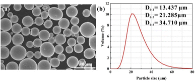
The received condition of Ag–Cu alloy powders depicted a nearly spherical shape and smooth surface. Importantly, no apparent agglomeration or porosity could be detected (Fig. 2a). The particle size of Ag–Cu powders varies from 13.437 to 34.710 μm, and the average diameter was 22.980 μm (Fig. 2b), similar to the size of diamond particles (25 μm). The sphere geometry and non-uniform size of Ag–Cu alloy particles increase the multiple scattering on highly reflective metal powder. This property can improve the absorption rate and enhance the bulk density of final fabricated parts.30 The chemical compositions of the Ag–Cu alloy were also characterised by SEM-EDS as an input parameter for the later simulation of the molten pool (Table 1). Although the mass fraction of Ag was 92.91 wt%, a little higher than the standard sterling silver (92.5 wt%), this slight content fluctuation of the Ag element was acceptable. The high quality of Ag–Cu powders favours high flowability and processability in SLM.| Chemical composition | Ag | Cu | C | W |
|---|---|---|---|---|
| Mass fraction (%) | 92.91 | 3.07 | 2.11 | 1.91 |
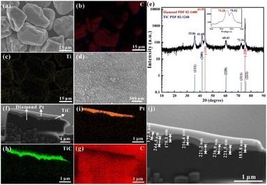
Due to the lack of affinity of the nonreactive system, the MMCs usually face the issue of low mechanical adhesion among different compositions.18,31 Therefore, to improve the wettability between metal matrix and diamond particles, the diamond particles used in this study were previously coated with Ti to prevent direct contact between the Ag–Cu alloy and diamond. Fig. 3a–c shows that Ti and C dominated the distribution of elements on the surface of diamond particles. Meanwhile, the distribution of Ti was continuous and uniform on the diamond surface. Further magnification of the surface demonstrated a fully dense and consolidated coating without any pores (Fig. 3d). The coating's quality was crucial for the fluidity of mixed Ag–Cu and diamond powders. In addition to the surface morphology, XRD was performed on the coated diamond particles (Fig. 3e). The pattern showed sharp peaks of 43.95° and 75.28° reflected (−1 1 1) and (−2 2 0), respectively, confirming the high degree of crystallinity of the diamond. It also indicated no damage to the crystal structure in the vacuum deposition process. Other peaks demonstrated the presence of cubic TiC (the reaction of Ti element and diamond particles during the coating process), which was consistent with the observation of short columnar TiC grains on the diamond surface in Fig. 3d.
Furthermore, the cross-sectional micrograph of the coated diamond was observed under SEM, and the Pt deposited layer was applied to protect the surface edges during the pretreatment process of FIB (Fig. 3f–i). The stepped bonding interface between the diamond particle and the coating layer indicated the tightly bonded Ti and diamond particles (Fig. 3h). According to the element mapping, Fig. 3h clearly shows TiC mapping. This composition was also detected in XRD (Fig. 3e). As a transition layer, there are two prominent roles to play for TiC: (i) it can prevent direct contact between the diamond filler and the Ag–Cu matrix during the SLM printing process, and both the flowability and the wettability of the mixed powders are improved;32 (ii) the interfacial bonding between both components allows a suitable thermal transfer from the Ag–Cu matrix to the diamond particles, avoiding the graphitisation of diamond particles.33,34 The depth of coating was analysed by the elemental distribution under SEM, ranging from 135.2 nm to 244.3 nm. The average thickness of the coating layer was approximately 209.6 nm. Moreover, this thickness allows for the performance enhancement of diamond particles without significantly increasing their volume.
Simulation of the molten pool
The single molten pool is a basic unit in the SLM-fabricated parts. Although the hatch distance and layer thickness affect grain growth and microstructural evolution, the heat transfer mechanism in the single molten pool is the deciding factor in the continuous manufacturing process. Therefore, the morphology and heat transfer were simulated in a single molten pool with different line energy densities (LED, J m−1, eqn (1)). Table 2 presents the detailed parameters. The dimension of the molten pool also increased with the increase in LED. Fig. 4 also illustrates this issue. Two main factors cause this phenomenon: (i) the heat accumulation effect caused by high laser power; and (ii) the longer interaction time between the powder bed and the laser beam under lower scanning speed.35 Importantly, the molten pool depth values were smaller than the tested results in a previous study.9,20 This occurred mainly because the laser heat source was simplified with the Gaussian heat flux on the surface. However, in real experiments, the laser can penetrate the powder bed on the pre-fabricated layers or the metal substrate to create a deeper molten pool.| Energy density | Laser power (W) | Scanning speed (mm s−1) | LED (J m−1) | Molten pool width (μm) | Molten pool depth (μm) |
|---|---|---|---|---|---|
| High | 120 | 400 | 300 | 183.2 | 112.1 |
| Medium | 120 | 1200 | 100 | 106.1 | 85.5 |
| Low | 40 | 1200 | 33 | 66.1 | 37.5 |
Generally, the heat transfer behaviour was nearly the same under different energy densities (Fig. 4). The red arrows represented the hot flow's direction, all of which were transferred along the normal direction of the bottom of the molten pool. Therefore, the temperature gradient was formed parallel to the opposite direction of the heat flow, and the largest temperature difference was perpendicular to the direction of the molten pool boundary. This kind of thermal transfer mechanism usually provided sufficient sharp heat accumulation for the growth of columnar grains along the building directions.
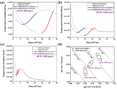
Because of the short interaction time between the laser beam and powder, liquid lifetime—the duration time from the melting of particles to the liquid–solid phase transformation and eventually solidification process—was introduced to examine the dynamic behaviour of molten pools under different energy densities.36,37 The temperature gradient in the centre and boundary region fluctuated and finally stabilised with the laser beam's movement (Fig. 5a–c). The solidification process occurred with the removal of the heat source. Moreover, the grain growth started immediately from the boundary to the centre area. It is worth noting that the relatively low scan speed or high laser power is usually accompanied by a longer liquid lifetime (Table 3). The main reason this occurs is that both higher laser power and lower scanning speed can enhance the energy density, leading to a higher temperature for the sufficient energy absorption of powder bed and a longer liquid lifetime to wet the surrounding particles. The duration of liquid as a molten pool does not change with the location—the centre area or boundary area—but changes with the input energy. As known, the duration of liquid as a molten pool decides the time of grain growth; therefore, the longer exposure time under high energy density will generate larger crystalline grain sizes.
| Liquid lifetime (ms) | Energy density (J m−1) | ||
|---|---|---|---|
| High | Medium | Low | |
| Centre area | 0.09 | 0.06 | 0.011 |
| Boundary area | 0.08 | 0.07 | 0.017 |
According to the classical theory of solidification kinetics,38 the primary grain microstructures of the given alloy are mainly determined by the local solidification condition of the molten pool, including the thermal gradient (G) and growth velocity (V). Generally, the G × V value is the cooling rate, which governs the scale of the solidification microstructure. The G/V ratio regulates the solidification model.39 Fig. 5d shows the simulation result. By comparing the calculated results of the boundary and centre of the molten pools, the increased G × V and decreased G/V values resulted from better heat dissipation efficiency at the boundary. The G × V value decided the size of the grains. With the increase of energy density, this value decreased, and the finer microstructure (grain space, size, interdendritic space, etc.) features could be obtained. A high G/V ratio corresponded to a stable planar front of crystallisation at low LED, whereas a low G/V ratio caused instability in the crystallisation front and dendritic solidification at a high energy input.
Formation of SLM-fabricated Ag–Cu/diamond composites
Microstructures analysis of SLM-fabricated Ag–Cu/diamond composites
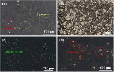
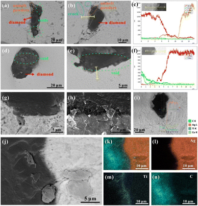
SEM-EDS was used to analyse the microstructures of cubic samples manufactured under different volume energy densities to observe the diamond particles' interface bonding and the Ag–Cu alloy matrix. Fig. 8a–b shows that the good bonded area between the diamond and matrix was only partially achieved under a high energy density. Although the high laser power was beneficial for improving the wettability of the diamond and metal matrix under a slight temperature gradient simulated in this study, it also inevitably caused thermal damage to the diamond or its coating—the Ti element was absent in cross-section joints according to the line scanning of EDS (Fig. 8c). Meanwhile, because of the large difference in the thermal expansion conductivity of diamond particles and the Ag–Cu matrix, strong internal stress will be generated in the bonding area under high temperatures, causing thermal cracks and then affecting the density of the surrounding metal matrix (Fig. 8b). The formation of inter-layer voids was usually accompanied by unmelted powders (Fig. 8a and b). The violent fluctuation and evaporation in the molten pool caused the spatter droplets, hindering the further processing with voids. These voids provided hiding places for unmelted powder in the spreading process (Fig. 8a).Some powders were hard to fully melt without sufficient energy input, especially near the diamond area, leading to the formation of voids (Fig. 8d and e). Although the interface integration between diamond particles and the Ag–Cu matrix was not ideal, the existence of the Ti element was detected with EDS (Fig. 8f). The excellent interface bonding between diamond particles and the Ag–Cu matrix requires sufficient time. Still, the short solidification time was simulated under the low energy density parameters. Creating a tight bond between the TiC coating and the metal matrix is challenging without adequate time.
The diamond particles were uniformly distributed in the Ag–Cu matrix without agglomeration under medium energy densities. The boundary of the diamond demonstrated a tight bonding to the surrounding metal matrix without any cracks or voids (Fig. 8g and h, j). The line scanning of EDS indicated that the Ti element diffused into the metal matrix to create a solid solution, and the thickness of the Ti-enriched layer ranged from 200 to 500 nm (Fig. 8i). According to the previous simulation results, it was speculated that in the late solidification period, the heat transfer from the diamond to the surrounding metal matrix was the primary driving force for inter-lattice atomic diffusion. Because the solid solubility of the Ti element in Ag was about 5%,42 the Ti at the interface could diffuse to the metal matrix, and the maximum diffusion distance was 4.6 μm based on the EDS test (Fig. 8m). The solidification time facilitated the formation of a strong bond between diamond and metal matrix and benefited the Ti diffusion (Fig. 8k–n). Therefore, the energy density was crucial for the chemical bonding of the Ag–Cu matrix and diamond particles.
Grain growth during SLM in Ag–Cu/diamond composites
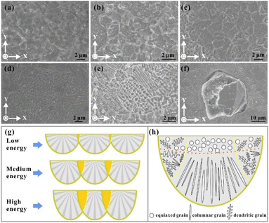
The equiaxed grains were usually observed on the top surfaces of the cubic parts (Fig. 9a–c). Meanwhile, the grain sizes of the equiaxed crystal varied with the input energy density—the sizes of grains decreased with the increase in the energy density, which was consistent with the simulated result. The grain size is believed to be determined by the cooling rate, which is also reflected in the G/V value, as demonstrated before in this study. Therefore, the high scanning speed and low laser power are beneficial to forming fine grains, and the average size could reach 800 nm under low energy density (Fig. 9a). Generally, the direction of grain growth is determined by its preferential orientation and the thermal gradient. The equiaxed grains were created under comparable driving forces in different directions, usually on the top surface of the molten pool, especially in the centre area (Fig. 9h).43 This happens because the thermal gradient along all directions is comparable to the top surface of the molten pool, and consistent simulated results are also obtained—the thermal gradient of the boundary and the centre of the molten pool were nearly the same.The dendritic grains (Fig. 9d) can also be observed on the horizontal section with a typical secondary structure. These grains usually grow in the overlap zone of the molten pools because of the multi-directional thermal gradients in the overlap area, providing the driving force for the growth of grains along multiple orientations and also restricting the further development of grains. Therefore, some directions of grain growth fully epitaxially develop, and others suffer early termination. Then, the dendritic crystal is formed. In contrast to the columnar grains, the dendrite grains are hard to grow in a single direction continually. Meanwhile, the several directions of grain growth usually conflict with each other, confining the formation of equiaxed grains.44
It is also worthwhile to point out that the input energy mainly decides the overlap rate of the molten pool. According to the hatch distance (h) and the width of the molten pool (w), the overlap rate of the molten pool (Hr) could be calculated as follows:
| h = (1 − Hr) × w | (10) |
The cross-section of the molten pool approximately resembled a semi-circular arc shape because of the distribution of the laser beam's energy as a Gaussian beam profile. As simulated in this study, the width of the molten pool increased with the increase in the energy density. Therefore, with a fixed hatch distance value (100 μm), the size of the overlap region also increased with the increase in the energy density (Fig. 9g). Therefore, several grain formations are usually present under a high energy input. Compared with the centre area, a longer liquid time, longer cooling rate and lower thermal gradient were observed under the Gaussian distribution of laser energy in the overlap areas between two molten pools, thereby promoting the development of secondary dendrite arms (Fig. 9d). The complex directions of the large temperature gradients contribute to the formation of various morphological grains in the overlap region (Fig. 9e). The equiaxed, dendritic and columnar crystals existed in this area, and the unique microstructural transition between equiaxed and dendritic grains was also generated. This kind of complex grain growth also appeared on the surrounding metal matrix of the diamond. Fig. 9h shows that the diamond particle shared a tight bond with the Ag–Cu metal. Therefore, because of the excellent heat transfer ability of the diamond, it influenced the thermal gradients around it and induced the formation of columnar grains—the size of these grains was also much shorter than that of the Z direction.
Distinctive columnar grains mainly grew along the Z direction, parallel to the building direction. They were also perpendicular to the bottom boundary of the molten pool (Fig. 10a). The simulation results demonstrated that the largest thermal gradient direction was along the normal direction of the molten pool, which provided a sufficient driving force for the growth of columnar crystals.45 Furthermore, the high thermal conductivity of the Ag–Cu alloy of the deposited layers also intensified the heat accumulation along the building direction. The preferred crystal orientation and the largest thermal gradient all along the same direction keep the grains from persistently growing in a single direction for a typical columnar morphology. As mentioned before in this study, the columnar grains also grew in the overlap area under complex thermal gradients. However, the size of these grains was smaller than that on the Z plane, accompanied by dendritic and columnar-dendritic grains. Notably, there are two directions for these grains, and they are perpendicular. They are explained from the beginning of grain solidification. Fig. 10 shows that a group of grains solidified on the N layer, and another group began to grow on the new track (N + 1 layer). The grains of the N layer had a preferential crystallographic orientation along21 with an arbitrary angle to the normal direction of the track boundary (white line in Fig. 10c). Chen et al.46 regarded a high φ value as related to a large angle between the growing direction in the N + 1 layer track and the direction opposite to the heat flux direction when the crystal growth direction was unchanged. Therefore, the growth direction of the grains in the new track (N + 1 layer) changed by 90° to another direction under a high φ angle to minimise the growth direction and the temperature gradient direction. In this case, the φ + θ = 90°.
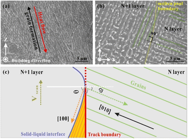 | ||
| Fig. 10 (a) Columnar grains on the Z direction (100 W, 1400 mm s−1); (b) columnar grains on the X–Y plane (100 W, 1400 mm s−1); (c) the schematic diagram of the columnar grain growth direction. | ||
Ag nanowires formation
Under low energy density, Ag nanowires were observed on the surface of SLM-fabricated samples (Fig. 11), especially on the X–Y plane. These nanowires prefer to grow on grain boundaries. Therefore, it is inevitable that these nanowires formed after the SLM process stopped instead of in the printing process. “Whisker formation” is well known as a highly localised stress relaxation mechanism.47,48 During SLM forming, the pressure stress mainly originates from two aspects: (i) residual stress caused by rapid cooling. Xiong et al.9 have shown that greater residual stress is generated under a low energy input with lower energy input and higher scanning speed; (ii) the compressive stress resulting from the diffusion of Cu at the grain boundary of the Ag–Cu alloy. During the high-speed cooling process of SLM, the Ag–Cu alloy rapidly precipitates as an α-silver solid solution phase.49,50 Then, during the solute redistribution process in the late solidification process, Cu atoms diffuse to the grain boundary of Ag and precipitate as the β-Cu alloy. Because of the difference in the relative density between Cu and Ag, compressive stress occurs spontaneously at the grain boundary. The stress induces recrystallisation at the grain boundaries, leading to cracks in oxide films. Also, under the restriction of oxide films, the lateral growth was hardly formed and the nanowire grew along single direction.51,52 Grains grow along the cracking areas to release the stress, finally forming whiskers. This is also the reason the Cu content in the whiskers (8.10 wt%) is significantly higher than that in the matrix (5.46 wt%). The enriched β-Cu at the boundary also reflects on the compositions of whiskers.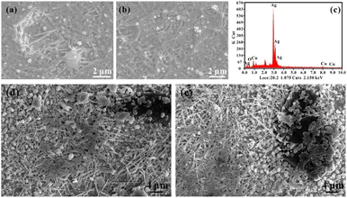 | ||
| Fig. 11 (a and b) Nanowires (40 W, 1000 mm s−1) with its EDS analysis (c); (d and e) nanowires near diamond (60 W, 1400 mm s−1). | ||
The whiskers are concentrated near the diamond particles (around 30–50 μm). Introducing diamond particles to the nuclei sites in the molten pool disperses the stress relief effect from the nanowires' growth. Hence, whiskers depict an intensive intertwined distribution. Meanwhile, compared with the pure Ag–Cu alloy without diamond under the same manufacturing conditions, the whiskers have a smaller length (8–12 μm) and width (70–150 nm).20 The addition of diamonds has a complicated effect on the growth of grains. The role of diamonds in the rapid solidification process of the composites can only be speculated. First, both the small laser spot of SLM (30 μm) and the diamond's size (25 μm) will restrict the rapid and continuous solidification of the metal molten pool, further leading to the rapid non-spontaneous nucleation and forced growth of the silver solid solution of α-Ag near diamond particles. It will also cause the formation of finer metal nuclei near the diamond. Meanwhile, due to the high absorptivity of diamond to 1064 nm of laser, it will increase to an extremely high temperature during the SLM process. The TiC coating with low thermal conductivity on the diamond surface limits the speed of heat transfer. This outcome will lead to a longer duration of the solid phase of Ag because it provides sufficient time for Cu atoms to fully precipitate at the grain boundary. Therefore, the precipitation of a large number of copper atoms provides more compressive stress, dramatically increases the nucleation probability of whisker nuclei, and provides more ways for stress release.
Conclusion
In this work, the first attempt was made to prepare Ag–Cu/diamond composites via SLM with several process parameters. The role of energy density during microstructural evolution, grain growth and nanowires growth was investigated theoretically and experimentally. With the addition of diamond, the over-melting region becomes larger than the pure Ag–Cu alloy, and the well-bonded interface of diamond particles and metal matrix mainly occurs in the low-medium energy density—the diffusion of Ti on the diamond coating (as far as 4.6 μm in the metal matrix). The equiaxed grain is prone to grow at the centre of the molten pool, and the input energy density influences its size—the higher the energy density, the longer the liquid lifetime for the larger grain formation, based on the simulated and experimental results. The addition of diamond also affects the thermal directions in the molten pool, and the complex grain growth occurs in the overlap area and the region surrounding the diamond particles. However, the development of columnar grains in the Z directions is not affected by the addition of diamond—it is still along the building directions and perpendicular to the bottom of the molten pool. The SLM process and the solute redistribution of Cu at the grain boundary cause the growth of interwoven nanowires (length: 8–12 μm; width: 70–150 nm) under high pressure and residual stress. This systematic analysis provides a comprehensive understanding of Ag–Cu/diamond composites and the relevant microstructural evolution and grain formation. It also allows for the controllable growth of Ag–Cu nanowires via SLM technology.Author contributions
Chenxing Xin: investigation, conceptualization, validation, and writing – original draft; Xiya Zhao: software and formal analysis; Haoze Geng: investigation, software, and methodology; Ping Gong: software; Liang Hao: supervision; Yan Li: supervision, project administration and funding acquisition; Tao Chen: formal analysis.Conflicts of interest
There are no conflicts to declare.Acknowledgements
The work was financially supported by Wuhan Applied Foundational Frontier Project (No. 2020010601012172) and National Natural Science Foundation of China (No. 51902295). The project was also supported by the “CUG Scholar” Scientific Research Funds at China University of Geosciences (Wuhan) (No. 2022185). Many thanks to the assistance of Prof. Tao Chen for FIB-SEM analysis. The publication of this article in 2022 marks the 30th anniversary of the Gemmological Institute and the 70th anniversary of the China University of Geosciences in Wuhan.References
- K. K. Chawla, in Composite materials, Springer, 2012, pp. 197–248 Search PubMed.
- P. Samal, P. R. Vundavilli, A. Meher and M. M. Mahapatra, J. Manuf. Process., 2020, 59, 131–152 CrossRef.
- X. Zhang, N. Q. Zhao and C. N. He, Prog. Mater. Sci., 2020, 113, 100672 CrossRef CAS.
- Y. G. Tong, Z. H. Cai, S. X. Bai, Y. L. Hu, M. Y. Hua, W. Xie, Y. C. Ye and Y. Li, Ceram. Int., 2018, 44, 16577–16582 CrossRef CAS.
- L. Yang, L. Sun, W. W. Bai and L. C. Li, Diamond Relat. Mater., 2019, 94, 37–42 CrossRef CAS.
- C. X. Li, X. T. Wang, L. H. Wang, J. W. Li, H. X. Li and H. L. Zhang, Mater. Des., 2016, 92, 643–648 CrossRef CAS.
- M. Sajjadnejad, H. Omidvar, M. Javanbakht and A. Mozafari, J. Alloys Compd., 2017, 704, 809–817 CrossRef CAS.
- F. Saba, F. Zhang, S. Liu and T. F. Liu, Compos. B. Eng., 2019, 167, 7–19 CrossRef CAS.
- W. Xiong, L. Hao, Y. Li, D. N. Tang, Q. Cui, Z. Y. Feng and C. Z. Yan, Mater. Des., 2019, 170, 107697 CrossRef CAS.
- S. Praiphruk, G. Lothongkum, E. Nisaratanaporn and B. Lohwongwatana, J. Met. Mater. Miner., 2013, 23, 67–73 CAS.
- Q. Li, H. Rao, H. Mei, Z. Zhao, W. Gong, A. Camposeo, D. Pisignano and X. Yang, Adv. Mater. Interfaces, 2022, 9, 2201175 CrossRef CAS.
- Q. Li, H. Rao, X. Yang, Z. Guo, W. Gong, X. Ma and B. Li, J. Phys. Chem. C, 2022, 126, 9293–9303 CrossRef CAS.
- M. Chen, L. Wen, D. Pan, D. R. Cumming, X. Yang and Q. Chen, Nanoscale, 2021, 13, 13024–13029 RSC.
- X. Yang and B. Li, Nanophotonics, 2020, 9, 1557–1577 CrossRef CAS.
- C. Y. Chen, Y. C. Xie, X. C. Yan, M. Ahmed, R. Lupoi, J. Wang, Z. M. Ren, H. L. Liao and S. Yin, Addit. Manuf., 2020, 36, 101434 CAS.
- L. Constantin, N. Kraiem, Z. P. Wu, B. Cui, J. L. Battaglia, C. Garnier, J. F. Silvain and Y. F. Lu, Addit. Manuf., 2021, 40, 101927 CAS.
- C. C. Tian, X. K. Li, H. Y. Li, G. Q. Guo, L. P. Wang and Y. M. Rong, Mater. Sci. Eng., A, 2019, 743, 697–706 CrossRef CAS.
- L. Constantin, L. S. Fan, M. Pontoreau, F. Wang, B. Cui, J. L. Battaglia, J. F. Silvain and Y. F. Lu, Manuf. Lett., 2020, 24, 61–66 CrossRef.
- J. Gan, H. Gao, S. F. Wen, Y. Zhou, S. C. Tan and L. C. Duan, Int. J. Refract. Met. Hard Mater., 2020, 87, 105144 CrossRef CAS.
- W. Xiong, L. Hao, T. Peijs, C. Z. Yan, K. K. Cheng, P. Gong, Q. Cui, D. N. Tang, S. Al Islam and Y. Li, Sci. Rep., 2022, 12, 4250 CrossRef CAS PubMed.
- J. H. Yi, J. W. Kang, T. J. Wang, X. Wang, T. Feng, Y. L. Feng and P. Y. Wu, Mater. Des., 2021, 197, 109259 CrossRef CAS.
- D. Tomus, P. A. Rometsch, M. Heilmaier and X. H. Wu, Addit. Manuf., 2017, 16, 65–72 CAS.
- S. W. Liu, H. H. Zhu, G. Y. Peng, J. Yin and X. Y. Zeng, Mater. Des., 2018, 142, 319–328 CrossRef CAS.
- J. Yin, H. H. Zhu, L. D. Ke, P. P. Hu, C. W. He, H. Zhang and X. Y. Zeng, Int. J. Adv. Manuf. Technol., 2016, 83, 1847–1859 CrossRef.
- Y. Liu, J. Zhang and Z. C. Pang, Opt. Laser Technol., 2018, 98, 23–32 CrossRef CAS.
- H. C. Tran and Y. L. Lo, J. Mater. Process. Technol., 2018, 255, 411–425 CrossRef.
- L. E. Loh, C. K. Chua, W. Y. Yeong, J. Song, M. Mapar, S. L. Sing, Z. H. Liu and D. Q. Zhang, Int. J. Heat Mass Transfer, 2015, 80, 288–300 CrossRef CAS.
- H. W. Hu, X. P. Ding and L. Z. Wang, Optik, 2016, 127, 8883–8891 CrossRef CAS.
- H. M. Khan, M. H. Dirikolu and E. Koc, Optik, 2018, 174, 521–529 CrossRef CAS.
- H. Attar, M. Bonisch, M. Calin, L. C. Zhang, S. Scudino and J. Eckert, Acta Mater., 2014, 76, 13–22 CrossRef CAS.
- L. Constantin, L. S. Fan, Q. M. Zou, B. Thomas, J. Roger, J. M. Heintz, C. Debiemme-Chouvy, B. Mortainge, Y. F. Lu and J. F. Silvain, Carbon, 2020, 158, 607–614 CrossRef CAS.
- X. Yang, L. Wen, J. Yan, Y. Bao, Q. Chen, A. Camposeo, D. Pisignano and B. Li, J. Phys. Chem. Lett., 2021, 12, 7034–7040 CrossRef CAS PubMed.
- Y. Zhang, H. L. Zhang, J. H. Wu and X. T. Wang, Scr. Mater., 2011, 65, 1097–1100 CrossRef CAS.
- T. Schubert, L. Ciupinski, W. Zielinski, A. Michalski, T. Weissgaber and B. Kieback, Scr. Mater., 2008, 58, 263–266 CrossRef CAS.
- Y. Li and D. Gu, Addit. Manuf., 2014, 1, 99–109 Search PubMed.
- P. P. Yuan and D. D. Gu, J. Phys. D: Appl. Phys., 2015, 48, 035303 CrossRef CAS.
- Z. Chen, Y. Xiang, Z. Wei, P. Wei, B. Lu, L. Zhang and J. Du, Appl. Phys. A, 2018, 124, 1–16 CrossRef.
- W. Kurz and D. J. Fisher, Fundamentals of solidification, CRC Press, Netherlands, 4 edn, 1984 Search PubMed.
- Z. Y. Liu, D. D. Zhao, P. Wang, M. Yan, C. Yang, Z. W. Chen, J. Lu and Z. P. Lu, J. Mater. Sci. Technol., 2022, 100, 224–236 CrossRef.
- E. Liverani, S. Toschi, L. Ceschini and A. Fortunato, J. Mater. Process. Technol., 2017, 249, 255–263 CrossRef CAS.
- Y. Tian, D. Tomus, P. Rometsch and X. Wu, Addit. Manuf., 2017, 13, 103–112 CAS.
- Z. M. Lei, H. Z. Zhang, E. L. Zhang, J. H. You, X. X. Ma and X. Z. Bai, Mater. Sci. Eng., C, 2018, 92, 121–131 CrossRef CAS PubMed.
- D. D. Gu, Q. M. Shi, K. J. Lin and L. X. Xi, Addit. Manuf., 2018, 22, 265–278 CAS.
- J. J. Yang, F. Z. Li, A. Q. Pan, H. H. Yang, C. Y. Zhao, W. P. Huang, Z. M. Wang, X. Y. Zeng and X. L. Zhang, J. Alloys Compd., 2019, 808, 151740 CrossRef CAS.
- X. Wang, C. H. Zhang, X. Cui, S. Zhang, J. Chen and J. B. Zhang, Mater. Charact., 2021, 174, 111020 CrossRef CAS.
- Z. W. Chen, M. A. L. Phan and K. Darvish, J. Mater. Sci., 2017, 52, 7415–7427 CrossRef CAS.
- A. Kosinova, D. Wang, P. Schaaf, A. Sharma, L. Klinger and E. Rabkin, Acta Mater., 2018, 149, 154–163 CrossRef CAS.
- M. Z. Liu, J. Tao, C. Y. Nam, K. Kisslinger, L. H. Zhang and D. Su, Nano Lett., 2014, 14, 5630–5635 CrossRef CAS PubMed.
- J. Sopousek, D. Drencakova, P. Broz, J. Bursik, A. Zemanova and P. Roupcova, J. Nanopart. Res., 2021, 23, 138 CrossRef CAS.
- Q. Li, H. Rao, X. Ma, H. Mei, Z. Zhao, W. Gong, A. Camposeo, D. Pisignano and X. Yang, Adv. Opt. Mater., 2022, 10, 2101976 CrossRef CAS.
- X. Yang, Y. Liu, H. Lei and B. Li, Nanoscale, 2016, 8, 15529–15537 RSC.
- X. Yang, D. Bao and B. Li, RSC Adv., 2015, 5, 60770–60774 RSC.
Footnote |
| † Electronic supplementary information (ESI) available. See DOI: https://doi.org/10.1039/d2ra05965g |
| This journal is © The Royal Society of Chemistry 2023 |

