
 Open Access Article
 This Open Access Article is licensed under a Creative Commons Attribution-Non Commercial 3.0 Unported Licence
Production of high-quality and large lateral-size black phosphorus nanoparticles/nanosheets by liquid-phase exfoliation
Haris Sarwar†
,
Peirui Ji†,
Shareen Shafique,
Xiaomin Wang and
Shuming Yang *
*
State Key Laboratory for Manufacturing Systems Engineering, Xi'an Jiaotong University, Xi'an, 710049, China. E-mail: shuming.yang@mail.xjtu.edu.cn
First published on 9th January 2023
Abstract
The liquid phase exfoliation (LPE) of layered black phosphorus (BP) material is essential in the field of electronics. N-Methyl-2-pyrrolidone (NMP) is one of the most promising precursors for obtaining BP nanosheets/nanoparticles, but the longer sonication time leads to smaller production of phosphorene. Herein, for the first time, the large lateral size fabrication of phosphorene was attained through NMP solvent by optimizing the process parameters. The resultant dispersions were characterized by atomic force microscopy, X-ray powder diffraction, Raman spectroscopy, scanning electron microscopy, transmission electron microscopy, and ultraviolet-visible spectroscopy. The characterization results revealed that the average lateral sizes of BP nanoparticles were found to be 67.8 ± 18.6 nm and the lateral size of fabricated BP nanosheets was found to be 5.37 μm. Moreover, this research provides a strategic approach for the mass production of phosphorene for photodetection applications.
1. Introduction
Recently, two-dimensional (2D) layered materials have gained much attention among researchers owing to their astonishing structural and chemical properties. Black phosphorus (BP) is a new promising 2D layered material that exhibits excellent potential in electronic and optoelectronic applications.1–4 In addition, 2D BP has a puckered honeycomb lattice due to its strong in-plane anisotropy.5,6 Generally, bulk BP crystals possess a vertical stack of phosphorene (single or few layers),7 which comprises weak van der Waals forces. Moreover, BP has a thickness-reliant layered band gap, which is different in the bulk crystal (0.3 eV) and single-layer phosphorene (2.0 eV).2,8 A tunable band gap is a vital factor, which makes BP a suitable 2D layered material in the applications of photodetectors,9–11 sensors,12,13 energy storage devices,14 lithium-ion batteries,15 and solar cells.16The exfoliation process is the basic route to explore the unique structural properties of 2D materials. Mechanical peeling is the best conventional method to obtain 2D products from bulk crystals. However, this method has low output yield and uncontrollable size, which is not suitable for high-efficiency mass production.17,18 On the other hand, liquid phase exfoliation (LPE) is an easy and cost-effective way to produce large-scale products.17 In the LPE process, the sonication or shearing of the bulk 2D material occurs in the presence of the precursor; therefore, selecting appropriate precursors holds great importance. To date, the exfoliation of bulk BP is effectively carried out in various organic solvents including N- methyl-2-pyrrolidone (NMP),19 dimethyl sulfoxide (DMSO),20 acetone,21 dimethylformamide (DMF),21 and N-cyclohexyl-2-pyrrolidone (CHP).22 Among them, NMP is proven to be the optimal organic solvent for the sonication of bulk BP.23,24 However, the long sonication time results in the degradation of phosphorene, which creates difficulty in achieving large-size and high-quality nanosheets.
Brent et al.19 explored the colloidal dispersion of a few-layered BP by sonication for 24 h in the presence of NMP, only a few hundred nanometres of nanosheets were obtained. Y. Liu et al.25 studied the production of BP nanosheets in NMP solvent through ice bath sonication for 6 h and produced nanosheets in the range of 100–500 nm. Z. C. Luo et al.26 fabricated a few layered BP nanosheets through bath sonication for 10 h in NMP, where the lateral sizes were found to be several hundred nanometres. Similarly, D. J. Late27 also synthesized BP nanosheets and nanoparticles in NMP precursor, however, the large sonication time (8 h) only produced 10 to 200 nm products. Recently, Tiouitchi G et al.28 obtained a 200.8 nm lateral size of phosphorene, at the sonication time of 12 h in NMP, through the bath ultrasonication process. Based on these studies, it is seen that the prolonged sonication time results in the smaller lateral size production of phosphorene through the LPE method. The improvements in the experimental process conditions including, sonication time, sizes of BP flakes, and sample handling time are of great significance. The large lateral size production of BP nanosheets/nanoparticles is quite inspiring for numerous applications like field effect transistors,29 photo-diodes,30 and BP-based hetero-structure devices.31 The efficient sample handling technique is also essential to the results. Therefore, there is a need for process optimization of nanomaterials where their desirable features can be successfully fabricated by planning economical techniques, manufacturing the maximum output in less time from fewer experiments. The particle size optimization is an essential feature, which can be controlled by temperature, concentration, chemical composition, the environment of production, and surface modifications.32,33
This research work has the following advantages. Firstly, it focuses on the optimization of the process parameters (crystal size, sonication time, power and frequency, and centrifugation time) in the LPE method by using an NMP precursor. Previously reported research work comprised of long sonication and centrifugation time which may hinder the large-size production of BP nanosheets/nanoparticles. This work presents a cost-effective and simple route for the fabrication of a few layers of phosphorene. Secondly, it aims to fabricate large lateral-size and high-quality BP nanosheets/nanoparticles for photodetection applications. In this work, the lateral size of fabricated BP nanosheets was found to be 5.37 μm, which is relatively larger than the previously stated works. Therefore, this work holds significance as large lateral size production of phosphorene by LPE is beneficial in fabricating photodetection devices as compared to the mechanical peeling method.
2. Experimental process
For the fabrication of BP nanosheets/nanoparticles, 20 mg of BP crystals powder was dispersed into 20 ml NMP precursor in a glass beaker. The glass beaker was placed carefully in the sonicator (Fisher FB 505). The mixture was sonicated (500 W, frequency of 20 kHz) for 90 minutes in an ambient condition. Afterward, the resultant mixture was centrifuged at 3000, 5000, and 8000 rpm for 20 minutes to obtain thin layers of phosphorene. Furthermore, the resultant dispersions were collected carefully. Fig. 1 illustrates the detailed experimental process for obtaining thin layers of phosphorene by the LPE method.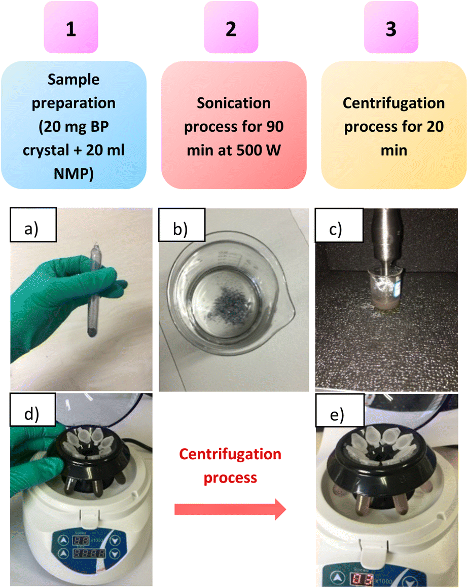 | ||
| Fig. 1 An illustration of the experimental procedure for exfoliating BP. (a) 2D BP stored in argon filled the glass tube, (b) sample preparation in a glass beaker (20 mg BP and 20 ml NMP precursor), (c) sonication process of 2D BP for 90 min at 500 W, (d) BP dispersions before centrifugation process and, (e) BP dispersions after centrifugation process. | ||
The LPE of layered BP material at different centrifugation speeds resulted in a change in phosphorene appearance. The black color sonicated dispersion is centrifuged at 3000 rpm (dark yellow), 5000 rpm (yellow), and 8000 rpm (pale yellow), as shown in Fig. 2. This change in dispersion color indicates varying thickness and lateral dimensions of phosphorene, at different centrifugation speeds. The as-prepared dispersions were collected and stored under N2 protection.
 | ||
| Fig. 2 (a) BP dispersions after sonication. (b) After centrifugation process at 3000, 5000, and 8000 rpm respectively. | ||
For effective and accurate identification of the surface analysis and size of the as-fabricated BP nanosheets/nanoparticles atomic force microscopy (AFM, Bruker Innova) was performed under ambient conditions. Herein, the supernatant with 8000 rpm dispersion was dropped on the surface of the Si/SiO2 (300 nm) substrate and spin-coated at 3000 rpm for 1 minute. Afterward, the sample was heated on the hot plate at 95 °C for 20 minutes to evaporate the NMP solvent. The surface scans were carried out in tapping mode and the cantilever beam was used. The Si probe was employed with the FESP (Bruker) probe model. Raman spectroscopy (Horiba JOBIN YVON, HR800) was accomplished at an excitation wavelength of 532 nm, with a laser pump at 2.331 eV and a numerical aperture of NA = 0.9 at room temperature. The spectra exhibited were in Stokes mode. The topology and surface characterizations were achieved by field emission scanning electron microscope (FESEM, GeminiSEM 500) and transmission electron microscope (TEM, JEOL JEM-2100). For SEM characterization, the sample was prepared by the spin coating process. The prepared BP nanosheets (8000 rpm) were drop casted on the Si/SiO2 (300 nm) substrate and heated on a hot plate at 85 °C for an appropriate time. For TEM, the preparation of the sample was accomplished by drop-casting the fabricated BP dispersion (8000 rpm) on the copper TEM grid. Then, the prepared samples were dried under light for 5 minutes to eliminate the NMP precursor. X-ray diffraction (XRD) (BRUKER D8 A25) was performed to explore the crystals' arrangements using Cu-Kα radiation. To further explore the optical properties of the bulk BP and fabricated dispersions, ultraviolet (UV)-visible spectroscopy measurements were performed using a spectrophotometer (Lambda750). During the sample preparation, the dispersions were put in the quartz cuvettes where the variation in the colors (dark brown for BP, yellow for 8000 rpm dispersion) was observed. The energy band gap (Eg) was estimated from absorption spectra using Tauc's plot (eqn (1)).34 The absorption coefficient (α) was calculated from eqn (2):
| ∝hv = A(hv − Eg)1/2 | (1) |
 | (2) |
3. Results and discussion
3.1. Characterization of BP nanosheets/nanoparticles
For obtaining precise knowledge about the surface morphology and the thickness of prepared phosphorene, AFM was performed. Fig. 3 displays the existence of thin layers of BP that endorses the successful exfoliation of bulk BP by the LPE method.19,28,35 The thickness of the selected regions (1 to 5) of prepared BP flakes is observed in Fig. 3(a). The inset of Fig. 3(a) reveals the vertical distance of the selected regions (1 to 5) which varies from 1.080 to 2.735 nm.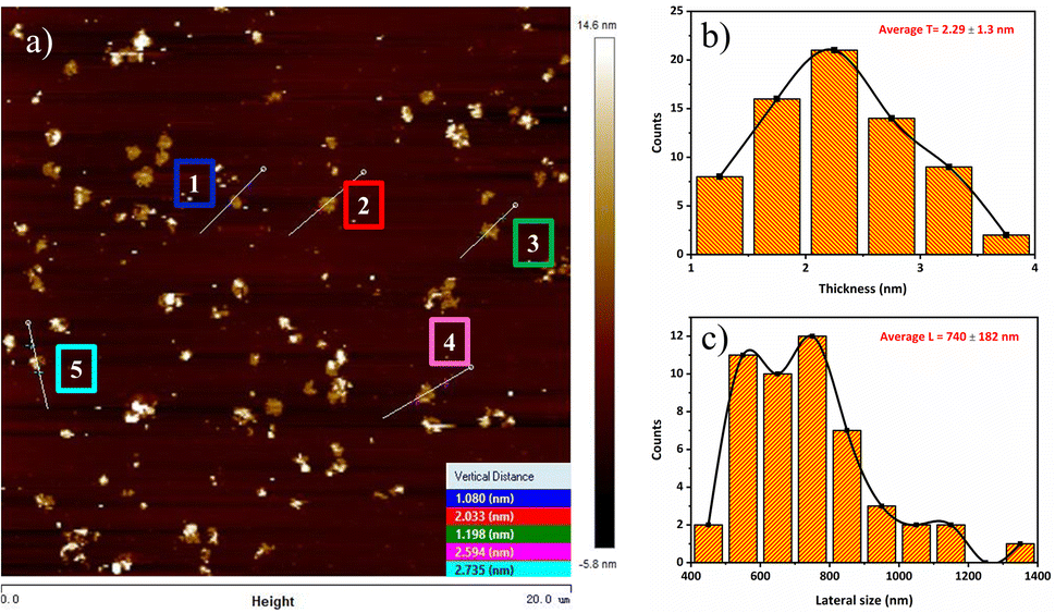 | ||
| Fig. 3 (a) AFM tapping phase image of BP flakes 8000 rpm dispersion spin-coated on Si/SiO2, (b) thickness profile of BP flakes, and (c) lateral size profile of BP flakes. | ||
Fig. 3(b) and (c) show the average thickness, and the average lateral size of a few layers of phosphorene, respectively. The average thickness and lateral size were found to be 2.29 ± 1.3 nm and 740 ± 182 nm by AFM measurement. The previous studies8,36 showed that the BP monolayer thickness was from 0.6 to 0.9 nm, and their lateral sizes were also small. AFM results revealed that most of the nanosheets consisted of 2 to 4 layers of phosphorene and the lateral sizes were much larger even at higher centrifugation speed.37 Brent et al.19 investigated the thickness of nanosheets which were in the range of 3.5–5 nm. AFM results reveal that most of the fabricated nanosheets are less than 2.5 nm, which provides strong evidence for the fabrication of thin layers of phosphorene. It should be noted that the shortest time between sample preparation and AFM measurement is the vital aspect for obtaining large lateral-size BP nanosheets.
Fig. 4(a) illustrates the exploration of the crystal arrangements of bulk BP crystal powders and the fabricated BP nanosheet dispersion by using the XRD method. At 16.9, 34.1, and 52.4°, the bulk BP crystal, and the fabricated BP nanosheets indicate three evident and thin peaks, which is related to the (020), (040), and (060) peaks position, respectively. As can be seen in the figure, the XRD peak position of the fabricated nanosheets is identical to that of the bulk BP crystal, but the peak intensity differs considerably from that of bulk BP.38,39 Therefore, the decrease in the XRD peaks of BP nanosheets approves the successful exfoliation of BP through the LPE method.
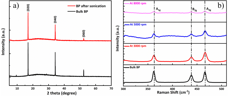 | ||
| Fig. 4 (a) Comparison of XRD patterns of bulk BP and fabricated BP supernatant after the sonication process. (b) Comparison of the Raman spectra between bulk BP crystals and fabricated BP dispersions after the centrifugation process (3000, 5000, and 8000 rpm, respectively). | ||
To confirm the successful exfoliation and determine the vibrational modes of fabricated phosphorene, Raman spectroscopy was performed. Fig. 4(b) shows the Raman spectrum comparison between bulk 2D BP crystal powder along with the fabricated BP dispersions at 3000, 5000, and 8000 rpm. Z. Guo et al.40 performed Raman measurements of phosphorene, where the three Raman peaks showed at 362.5 cm−1, 439.3 cm−1, and 467.6 cm−1. As can be seen in Fig. 4(b), three Raman peaks are observed at 361.8 cm−1, 438.3 cm−1, and 466.5 cm−1 concerning their phonon modes A1g, B2g, and A2g. Raman spectrum illustrates that the peak values are in good accordance with the previous studies41,42 which approve the successful exfoliation of bulk BP by the LPE method. It is noted that the characteristics peaks intensity of prepared dispersions at 3000, 5000, and 8000 rpm are weakened as compared to bulk BP peak, which is clear evidence in the reduction of thickness and lateral size of the nanosheets.28 The thickness reduction effect of LPE method will cause an increment of bandgap probably due to the decrease of grain crystal size, which may result in changes in atomic distances.2 The results demonstrate that higher centrifugation speed could not influence the peaks shift,40,43 thus the as-prepared phosphorene upholds high crystalline nature. Raman spectroscopy can also be used to adjust the alteration in controlling the process parameters for achieving thin layers and high-quality phosphorene.
BP nanoparticles were observed to show platelet-like structures with non-uniform sizes at the scale of 0.5 μm (shown in Fig. 5(a)). A similar structure was reported by Sofer et al.,23 where BP nanoparticles were prepared by the chemical vapor transport method. According to Fig. 5(b), well-dispersed BP nanoparticles with a lateral size of around 30–120 nm were observed, which indicated the large lateral size production of BP nanoparticles through NMP precursor. The average lateral sizes were calculated to be 67.8 ± 18.6 nm. This was further confirmed by L. Wang et al.,44 where BP nanoparticles were prepared by sonication-assisted hydrothermal method, and the obtained size was small (around 30 nm). K. Du et al.45 also explored the exfoliation of BP crystals in ethanol precursor through microwave-supported LPE technique and achieved an average thickness of 2.19 ± 1.33 nm for BP dots. Fig. 5(c) and (d) show the SEM morphologies of fabricated BP nanosheets, where the lateral size is found to be 3 μm and 1.7 μm, respectively, which confirms the large lateral size fabrication of phosphorene. HRTEM images (Fig. 6(a)) further showed clear lattice fringes of BP nanosheets. The corresponding selected area electron diffraction (SAED) pattern (Fig. 6(c)) was comprised of distinct spots demonstrating the high crystalline and orthorhombic nature of the produced nanosheets. The sheets size profile (Fig. 6(b)) complemented the SEM results as high-quality BP nanosheets were prepared, with the largest sheet size of 5.37 μm. Previous studies report19,31,42,46 that the lateral dimensions of BP nanosheets were in the range of hundreds of nanometres, while the results in this study are greatly improved. Therefore, the TEM, HRTEM, and SEM results demonstrated that the large lateral size production of BP nanosheets/nanoparticles could be easily achieved through the LPE process. The large lateral size can provide an essential route for the exploration of optoelectronic properties in BP-based devices. It should also be noted that a large size of BP nanosheets/nanoparticles can be attained by improving the sample handling procedure in the LPE process. According to previous studies in Table 1, the process optimization parameters are not favorable as large sonication times and non-invasive methods like bath sonication have been used. However, this study used an effective probe sonication technique with less time and frequency to produce large lateral sizes of BP nanoparticles, which are beneficial for their practical implementations.
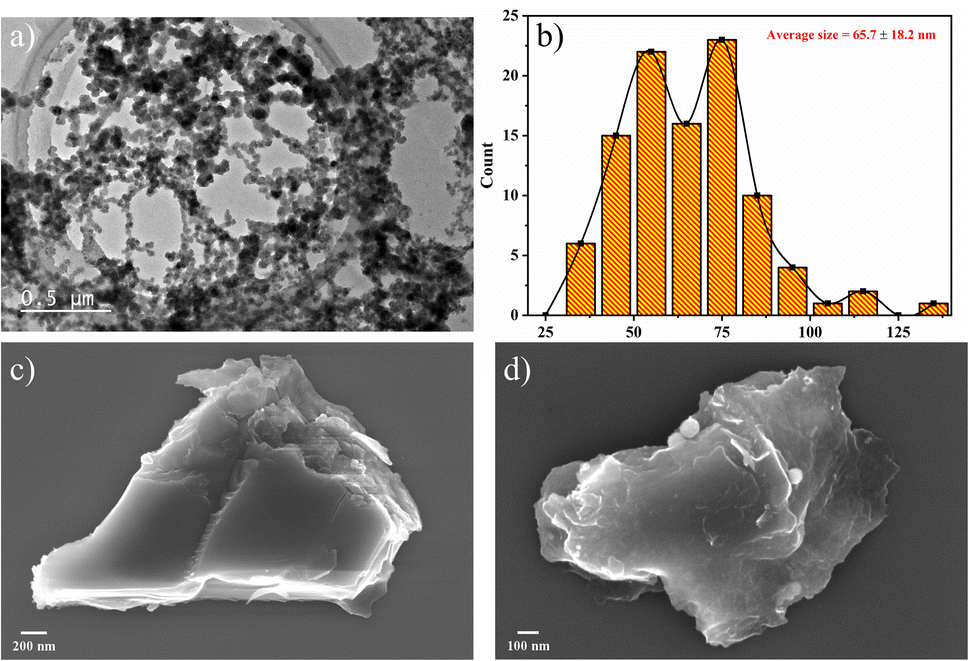 | ||
| Fig. 5 (a) TEM image of non-uniform sizes of BP nanoparticles at 0.5 μm scale, (b) the corresponding particle-size profile, (c) and (d) SEM images of fabricated BP nanosheets. | ||
 | ||
| Fig. 6 (a) HRTEM images of fabricated BP nanosheets at 8000 rpm dispersion, (b) the corresponding nanosheets size profile, and (c) the SAED pattern of the TEM sample. | ||
| Solvents | Sonication type | Sonication time | Sonication power | Sonication frequencya | Centrifugation time | BP size obtained | Ref. |
|---|---|---|---|---|---|---|---|
| a —Not mentioned in the literature. | |||||||
| NMP | Bath | 24 h | 820 W | 37 kHz | 45 min | 200 nm | 19 |
| DMF | Probe | 15 h | 130 W | — | 30 min | 190 nm | 20 |
| CHP | Probe | 5 h | 750 W | — | 180 min | 500 nm | 22 |
| NMP | Bath | 8 h | 110 W | 40 kHz | 15 min | 200 nm | 27 |
| Acetone | Bath | 10 h | 300 W | — | 60 min | 600 nm | 47 |
| NMP | Probe | 1.5 h | 500 W | 20 kHz | 20 min | 5.37 μm | This work |
3.2. Absorption measurement and Tauc plot analysis
For practical implementation of the as-fabricated BP nanosheets/nanoparticles, the optical properties were explored by ultraviolet (UV)-visible spectroscopy. The variation in the dispersion colors (dark brown for BP, yellow for 8000 rpm) was observed during the sample preparation.16,48 It can be noted from Fig. 7(a) that at high wavelengths, the absorbance intensity decreases with increasing rpm,36,45,49 because of the thickness reduction in the dispersion, this supported the Raman results in Fig. 4(b). The Tauc plot in Fig. 7(b) displays the linear dependent increase in the photon energy (hν) to band gap energy (eV). The Tauc figure reveals that the band gap (Eg) of BP is 1.96 eV, which is related to the optical band gap of 2D BP. W. Chen et al.16 investigated the band gap of BP quantum dots, which was derived to be 2.25 eV. Moreover, X. Niu et al.35 also observed the band gap of BP dots, which was calculated to be 2.1 eV. The results indicate that the band gap of fabricated 2D BP is in accordance with the literature. It is worth noting that the band gap of 8000 rpm dispersion is calculated to be 3.31 eV, which is larger than the band gap of 2D BP (1.96 eV), which confirms the thickness reduction by the LPE method. Tauc plot results demonstrate that a wide range of absorption spectra (UV to NIR) can be achieved if the process parameters are improved. | ||
| Fig. 7 (a) Absorption spectrum of bulk BP and the 8000 rpm dispersion, (b) Tauc plots of bulk BP and the 8000 rpm dispersion. | ||
4. Conclusions
In this work, the LPE of layered BP was carried out in NMP solvent via improved process parameters for obtaining large lateral-size phosphorene. The BP crystals powder was sonicated for 90 min and centrifuged at different speeds for 20 min under ambient conditions. BP nanosheets/nanoparticles were characterized by AFM, SEM, TEM, HRTEM, and Raman spectroscopy. The results showed that the fabricated phosphorene comprised 2 to 4 layers with an average thickness of 2.29 ± 1.3 nm. The lateral size of obtained BP nanosheets was 5.37 μm, while the average size of BP nanoparticles was found to be 67.8 ± 18.6 nm, which confirms the large lateral size production of BP nanosheets/nanoparticles. Large sonication time may result in the degradation of phosphorene, therefore, in this work, less sonication time has been set, which demonstrates that the process parameters are the vital steps in attaining large lateral size and high-quality phosphorene. The as-fabricated BP nanosheets/nanoparticles is quite inspiring for numerous applications like field effect transistors, photo-diodes, and BP-based hetero-structure devices. The practical implementation of these nanosheets will be the future course of this research.Conflicts of interest
There are no conflicts of interest to declare.Acknowledgements
The authors would like to acknowledge the support by the National Science Fund for Distinguished Young Scholars (52225507), and the Fundamental Research Funds for the Central Universities for their support.References
- J. Qiao, X. Kong, Z.-X. Hu, F. Yang and W. Ji, Nat. Commun., 2014, 5, 4475 CrossRef CAS.
- V. Tran, R. Soklaski, Y. Liang and L. Yang, Phys. Rev. B: Condens. Matter Mater. Phys., 2014, 89, 235319 CrossRef.
- J. Miao, L. Zhang and C. Wang, 2D Mater., 2019, 6, 032003 CrossRef.
- X. Wang and S. Lan, Adv. Opt. Photon., 2016, 8, 618–655 CrossRef.
- R. Gusmão, Z. Sofer and M. Pumera, Angew. Chem., Int. Ed., 2017, 56, 8052–8072 CrossRef.
- S. Lan, S. Rodrigues, L. Kang and W. Cai, ACS Photonics, 2016, 3, 1176–1181 CrossRef.
- L. Kou, C. Chen and S. C. Smith, J. Phys. Chem. Lett., 2015, 6, 2794–2805 CrossRef.
- H. Liu, A. T. Neal, Z. Zhu, Z. Luo, X. Xu, D. Tománek and P. D. Ye, ACS Nano, 2014, 8, 4033–4041 CrossRef CAS PubMed.
- X. Ren, Z. Li, Z. Huang, D. Sang, H. Qiao, X. Qi, J. Li, J. Zhong and H. Zhang, Adv. Funct. Mater., 2017, 27, 1606834 CrossRef.
- K. Chen, Y. Wang, J. Liu, J. Kang, Y. Ge, W. Huang, Z. Lin, Z. Guo, Y. Zhang and H. Zhang, Nanoscale, 2019, 11, 16852–16859 RSC.
- P. Ji, S. Yang, Y. Wang, K. Li, Y. Wang, H. Suo, Y. T. Woldu, X. Wang, F. Wang, L. Zhang and Z. Jiang, Microsyst. Nanoeng., 2022, 8, 9 CrossRef PubMed.
- Y. Wang, Y. Zhou, H. Ren, Y. Wang, X. Zhu, Y. Guo and X. Li, Anal. Chem., 2020, 92, 11007–11017 CrossRef PubMed.
- Y. Wang, J. Xue, X. Zhang, J. Si, Y. Liu, L. Ma, M. ullah, M. Ikram, L. Li and K. Shi, Mater. Sci. Semicond. Process., 2020, 110, 104961 CrossRef.
- G. Zhao, T. Wang, Y. Shao, Y. Wu, B. Huang and X. Hao, Small, 2017, 13, 1602243 CrossRef PubMed.
- L. Chen, G. Zhou, Z. Liu, X. Ma, J. Chen, Z. Zhang, X. Ma, F. Li, H.-M. Cheng and W. Ren, Adv. Mater., 2016, 28, 510–517 CrossRef PubMed.
- W. Chen, K. Li, Y. Wang, X. Feng, Z. Liao, Q. Su, X. Lin and Z. He, J. Phys. Chem. Lett., 2017, 8, 591–598 CrossRef CAS PubMed.
- S. Lin, Y. Chui, Y. Li and S. P. Lau, FlatChem, 2017, 2, 15–37 CrossRef.
- Z. Luo, J. Maassen, Y. Deng, Y. Du, R. P. Garrelts, M. S. Lundstrom, P. D. Ye and X. Xu, Nat. Commun., 2015, 6, 8572 CrossRef PubMed.
- J. R. Brent, N. Savjani, E. A. Lewis, S. J. Haigh, D. J. Lewis and P. O'Brien, Chem. Commun., 2014, 50, 13338–13341 RSC.
- P. Yasaei, B. Kumar, T. Foroozan, C. Wang, M. Asadi, D. Tuschel, J. E. Indacochea, R. F. Klie and A. Salehi-Khojin, Adv. Mater., 2015, 27, 1887–1892 CrossRef PubMed.
- A. E. Del Rio Castillo, V. Pellegrini, H. Sun, J. Buha, D. A. Dinh, E. Lago, A. Ansaldo, A. Capasso, L. Manna and F. Bonaccorso, Chem. Mater., 2018, 30, 506–516 CrossRef.
- D. Hanlon, C. Backes, E. Doherty, C. S. Cucinotta, N. C. Berner, C. Boland, K. Lee, A. Harvey, P. Lynch, Z. Gholamvand, S. Zhang, K. Wang, G. Moynihan, A. Pokle, Q. M. Ramasse, N. McEvoy, W. J. Blau, J. Wang, G. Abellan, F. Hauke, A. Hirsch, S. Sanvito, D. D. O'Regan, G. S. Duesberg, V. Nicolosi and J. N. Coleman, Nat. Commun., 2015, 6, 8563 CrossRef PubMed.
- Z. Sofer, D. Bouša, J. Luxa, V. Mazanek and M. Pumera, Chem. Commun., 2016, 52, 1563–1566 RSC.
- J. Kang, J. D. Wood, S. A. Wells, J.-H. Lee, X. Liu, K.-S. Chen and M. C. Hersam, ACS Nano, 2015, 9, 3596–3604 CrossRef PubMed.
- Y. Liu, W. Qi, S. Gong, J. He, Z. Li and Y. Li, Phys. B, 2020, 579, 411903 CrossRef.
- Z.-C. Luo, M. Liu, Z.-N. Guo, X.-F. Jiang, A.-P. Luo, C.-J. Zhao, X.-F. Yu, W.-C. Xu and H. Zhang, Opt. Express, 2015, 23, 20030–20039 CrossRef PubMed.
- D. J. Late, Microporous Mesoporous Mater., 2016, 225, 494–503 CrossRef.
- G. Tiouitchi, M. A. Ali, A. Benyoussef, M. Hamedoun, A. Lachgar, A. Kara, A. Ennaoui, A. Mahmoud, F. Boschini, H. Oughaddou, A. El Moutaouakil, A. El Kenz and O. Mounkachi, R. Soc. Open Sci., 2020, 7, 201210 CrossRef PubMed.
- P. J. Jeon, Y. T. Lee, J. Y. Lim, J. S. Kim, D. K. Hwang and S. Im, Nano Lett., 2016, 16, 1293–1298 CrossRef PubMed.
- L. Wang, X. Zou, J. Lin, J. Jiang, Y. Liu, X. Liu, X. Zhao, Y. F. Liu, J. C. Ho and L. Liao, ACS Nano, 2019, 13, 4804–4813 CrossRef PubMed.
- K. Ge, Y. Zhang, D. Wang, Z. Li, J. He, C. Fu, Y. Yang, M. Pan and L. Zhu, ACS Appl. Mater. Interfaces, 2020, 12, 20035–20043 CrossRef PubMed.
- J. Zou, W. Luo, S. Wang and Y. Wang, Zhongnan Daxue Xuebao, Yixueban, 2022, 47, 1398–1407 Search PubMed.
- C. Muthukumar, M. Changmai, S. Vincent, K. Raju, J. Mathai, S. Damale and B. G. Prakash Kumar, J. Cleaner Prod., 2022, 371, 133616 CrossRef.
- R. K. Ratnesh and M. S. Mehata, AIP Advances, 2015, 5, 097114 CrossRef.
- X. Niu, Y. Yu, J. Yao, M. Li, J. Sha and Y. Wang, Chem. Phys. Lett., 2021, 772, 138571 CrossRef.
- Y. Zhang, N. Dong, H. Tao, C. Yan, J. Huang, T. Liu, A. W. Robertson, J. Texter, J. Wang and Z. Sun, Chem. Mater., 2017, 29, 6445–6456 CrossRef.
- C.-H. Choi, Y.-J. Park, X. Wu and D.-P. Kim, Chem. Eng. J., 2018, 333, 336–342 CrossRef.
- H. Ma, J. Liu, Y. Wang, S. Zuo, Y. Yu and B. Li, Mater. Adv., 2022, 3, 7546–7558 RSC.
- M. Khurram, Z. Sun, Z. Zhang and Q. Yan, Inorg. Chem. Front., 2020, 7, 2867–2879 RSC.
- Z. Guo, H. Zhang, S. Lu, Z. Wang, S. Tang, J. Shao, Z. Sun, H. Xie, H. Wang, X.-F. Yu and P. K. Chu, Adv. Funct. Mater., 2015, 25, 7100 CrossRef.
- H. Wang, X. Yang, W. Shao, S. Chen, J. Xie, X. Zhang, J. Wang and Y. Xie, J. Am. Chem. Soc., 2015, 137, 11376–11382 CrossRef CAS PubMed.
- D. Yu, J. Li, T. Wang, X. She, Y. Sun, J. Li, L. Zhang, X.-F. Yu and D. Yang, Phys. Status Solidi Rapid Res. Lett., 2020, 14, 1900697 CrossRef CAS.
- Z. Yan, X. He, L. She, J. Sun, R. Jiang, H. Xu, F. Shi, Z. Lei and Z.-H. Liu, J. Materiomics, 2018, 4, 129–134 CrossRef.
- L. Wang, Y. Hu, F. Qi, L. Ding, J. Wang, X. Zhang, Q. Liu, L. Liu, H. Sun and P. Qu, ACS Appl. Mater. Interfaces, 2020, 12, 8157–8167 CrossRef CAS PubMed.
- K. Du, W. Yang, S. Deng, X. Li and P. Yang, Nanomaterials, 2020, 10, 139 CrossRef CAS.
- W. Zhao, Z. Xue, J. Wang, J. Jiang, X. Zhao and T. Mu, ACS Appl. Mater. Interfaces, 2015, 7, 27608–27612 CrossRef CAS.
- C. Hao, B. Yang, F. Wen, J. Xiang, L. Li, W. Wang, Z. Zeng, B. Xu, Z. Zhao, Z. Liu and Y. Tian, Adv. Mater., 2016, 28, 3194–3201 CrossRef CAS.
- Y. Xu, Z. Wang, Z. Guo, H. Huang, Q. Xiao, H. Zhang and X.-F. Yu, Adv. Opt. Mater., 2016, 4, 1223–1229 CrossRef CAS.
- S. P. Ogilvie, M. J. Large, G. Fratta, M. Meloni, R. Canton-Vitoria, N. Tagmatarchis, F. Massuyeau, C. P. Ewels, A. A. K. King and A. B. Dalton, Sci. Rep., 2017, 7, 16706 CrossRef PubMed.
Footnote |
| † These authors contributed equally to this work. |
| This journal is © The Royal Society of Chemistry 2023 |