
 Open Access Article
 This Open Access Article is licensed under a
 Creative Commons Attribution 3.0 Unported Licence
Scale-up synthesis of high-quality solid-state-processed CsCuX (X = Cl, Br, I) perovskite nanocrystal materials toward near-ultraviolet flexible electronic properties†
Zhi Jiang ab,
Hezhuang Liub,
Jihua Zoub,
Yixuan Huangb,
Zhaoquan Xub,
Denys Pustovyia and
Svetlana Vitusevich*a
ab,
Hezhuang Liub,
Jihua Zoub,
Yixuan Huangb,
Zhaoquan Xub,
Denys Pustovyia and
Svetlana Vitusevich*a
aInstitute of Biological Information Processing (IBI-3), Forschungszentrum Jülich, Leo-Brandtstr, 52425 Jülich, Germany. E-mail: s.vitusevich@fz-juelich.de; z.jiang@fz-juelich.de
bInstitute of Fundamental and Frontier Sciences, No. 4, Sec. 2, North Jianshe Rd., 610054 Chengdu, China
First published on 20th February 2023
Abstract
High-quality CsCu2X3 and Cs3Cu2X5 (X = Cl, Br, I) nanocrystals (NCs) exhibit excellent optoelectronic, physical, and chemical properties for detection of UV radiation due to large carrier mobility and lifetime, and heavy atoms. The nanocrystal materials can be prepared via a low-cost and simple solid-state synthesis. However, poor reproducibility and complex synthesis methods of obtaining perovskite NC thin films represent a drawback for the fabrication of the commercial photoelectric device. To address these issues, we develop highly stable CsCu2X3 and Cs3Cu2X5 NC materials using a facile solid-state reaction method for the scale-up production of halogen lead-free perovskites. We suggest a distinctive way to design a series of nanocrystalline perovskites using short-term synthesis and study the mechanism of perovskite formation using thermal solid-state synthesis. These all-inorganic and lead-free CsCu2X3 and Cs3Cu2X5 exhibit large photoluminescence quantum yields (PLQYs) up to 95.2%. Moreover, flexible paper photodetectors based on this series of lead-free perovskites show strong photoselectivity and bending stability at 254 nm, 365 nm, and 405 nm wavelengths. High-quality responses with a responsivity of 1.1 × 10⁻³ A W−1 and detectivity of 2.71 × 10⁹ jones under UV illumination (10 μW cm−2) at a bias voltage of 5 mV are demonstrated. These results open prospects for designing photodetectors, LEDs, and other photosensitive devices.
Introduction
Organic–inorganic metal halide perovskites and formamidinium lead halide (FAPbX3) perovskites (PVs) have attracted substantial interest,1–6 owing to their excellent optical properties, including superior photoluminescence quantum yields (PLQYs),5–7 tunable bandgap,8 ease of processability and small exciton binding energy.9–11 All-inorganic lead-containing halides CsPbX3 (ref. 12) have been widely employed as efficient active materials in solar cells, light-emitting diodes and photodetectors.13–15 However, the key issue of these materials is their instability in ambient conditions related to the organic component. On the other hand, the toxicity of lead (Pb) element is another concern because Pb is a hazardous material. As to PV application, electrical characteristics of electronic devices on flexible printable substrate16 may deteriorate due to external deformation and surface roughness. The change in device shape may produce surface tension and even defects, which result in weakening the photoelectric properties of photodetectors. Although all-inorganic low-dimensional metal halides demonstrate relatively high thermal stability, photoelectric properties of such materials still suffer from low responsivity (R) and detectivity (D*) even at ultra-low operation voltage.17The development of new environmentally-friendly materials without organic lead halide compounds is critical for future photovoltaic and display technologies18–20 Numerous groups developed alternative lead-free and organic–inorganic halide perovskites in recent years. Cesium (Cs)-based perovskite nanocrystals (NCs) crystallization technique could utilize suitable solvents to satisfy the need for a diverse variety of crystal geometries and to replace organic materials MA/FA and Pb in the perovskite lattice, such as zero-dimensional (0D) Cs3Cu2X5 NCs21 and subsequent crystallization,22 inverse temperature crystallization strategy.23,24 Unfortunately, lead-free perovskite NCs suffer from another possible obstacle. These organic–inorganic perovskite NCs and photodetectors based on them still suffered from short-term instability under wet conditions, complex process technology, and a small production rate.25 It is necessary to develop high-performance, low-cost, gram-scale all-inorganic and lead-free metal halide salts,26 using such methods as a hot one-pot solution synthesis27 and a solvent-free mechanochemical approach.28 A facile all-inorganic halide perovskite solid-state reaction method was reported by Huang29 and Roccanova.30
The method is useful and promising to synthesize high-quality Cs lead-free copper (Cu) inorganic metal halide PVs. Low-dimensional metal halide perovskites: CsCu2X3 and Cs3Cu2X5 (X = Cl, Br, I) exhibited fine stability in the atmospheric environment.31–33 Although the synthesis and bulk properties of low-dimensional Cs copper halides have been reported, the studies about a wide range of compositional variations of halogen anions and the material application as photodetector on flexible substrates are limited at present.34,35 This solid-state reaction technique can be considered as environmentally friendly chemistry because it does not involve the utilization of solvents.
In this paper, orthorhombic single-crystalline lead-free copper halide salts based on CsCu2X3 and Cs3Cu2X5 are synthesized by reacting stoichiometric amounts of CsX and CuX (X = Cl, Br, I) using solid-state reaction method for the scale-up halogen lead-free perovskites. High-quality properties are demonstrated for PV devices fabricated on a flexible substrate.
Results and discussion
All-inorganic lead-free perovskites were synthesized via a thermal solid-state method, as schematically illustrated in Fig. 1a. The details of growth procedure and synthesis procedure are given in the Experimental section. Briefly, the raw materials were mixed in a glovebox and then after temperature optimization calcined at 400 °C (except CsCu2Br3 material, which was calcined at 550 °C) for 6 h in a tube furnace to obtain ultra-stable NC materials. This step is finalized by the natural cooling process. The NC films were subsequently fabricated by spin coating the precursor dissolved in N,N-dimethylformamide (DMF), deposited on a paper substrate and annealing at 100 °C Fig. 1d. By precisely controlling the stoichiometric ratio of CsX![[thin space (1/6-em)]](https://www.rsc.org/images/entities/char_2009.gif) :CuX powders, the high-quality single crystalline CsCu2X3 and Cs3Cu2X5 nanocrystals (NCs) can be obtained, as displayed results in Fig. 1–3. A clear colour change (including green, blue, violet and yellow) over the entire visible range could be controlled owing to the variation of optical absorbance and PL emission. These different photoluminescence spectra emitted from various PV NC powders under UV illumination indicate the formation of tunable bandgaps via facile composition engineering.
:CuX powders, the high-quality single crystalline CsCu2X3 and Cs3Cu2X5 nanocrystals (NCs) can be obtained, as displayed results in Fig. 1–3. A clear colour change (including green, blue, violet and yellow) over the entire visible range could be controlled owing to the variation of optical absorbance and PL emission. These different photoluminescence spectra emitted from various PV NC powders under UV illumination indicate the formation of tunable bandgaps via facile composition engineering.
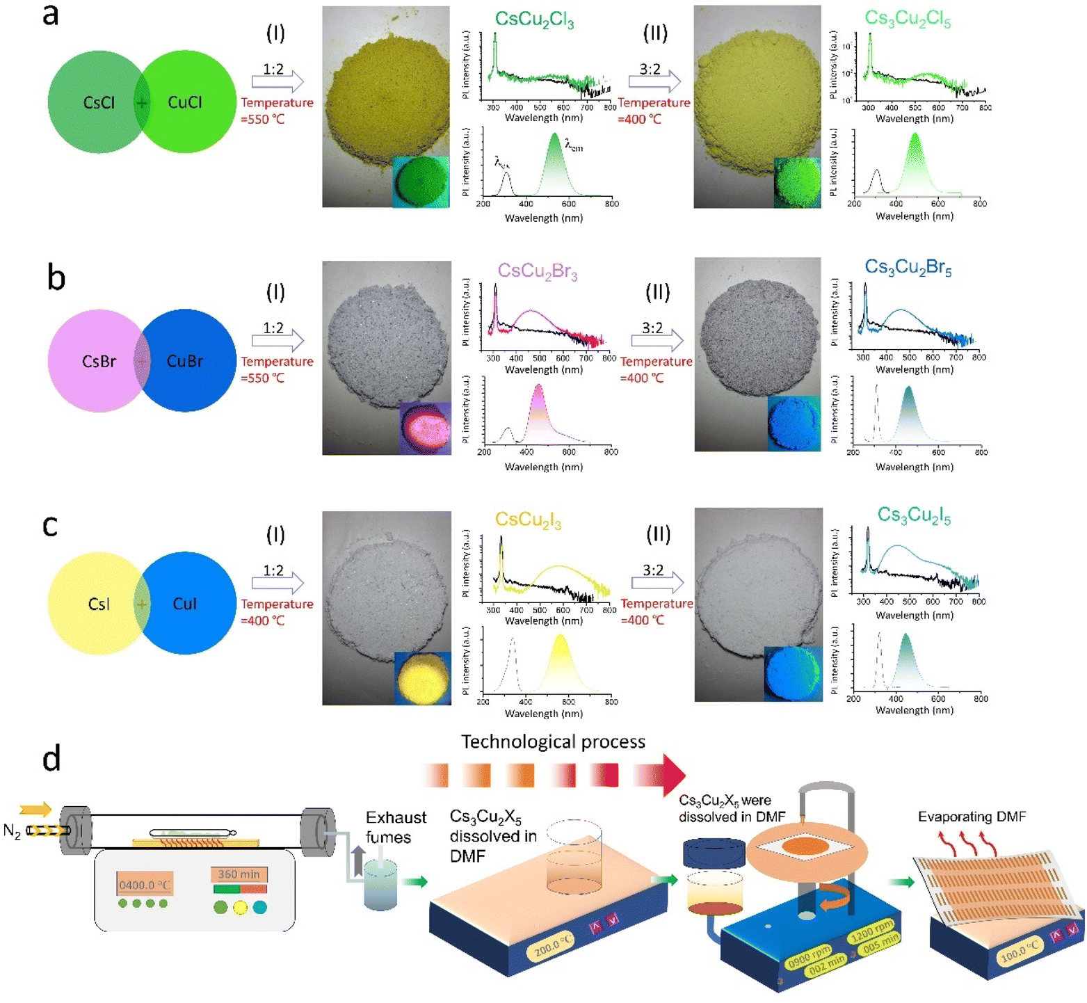 | ||
| Fig. 1 Schematic of typical solid-phase reactions for obtaining all-inorganic lead-free perovskite NC materials, demonstration of excitation of BaSO4 line of reference spectrum and emission spectrum, and the corresponding photoluminescence excitation (PLE) and photoluminescence emission (PL). (a) CsCu2Cl3 and Cs3Cu2Cl5 NCs, (b) CsCu2Br3 and Cs3Cu2Br5 NCs, (c) CsCu2I3 and Cs3Cu2I5 NCs. (I) Images of perovskite powder under ambient light (large grey/dark yellow circles) and (II) UV light irradiation (small color circles), the scale bars of 1 cm. (d) Schematic presentation of the fabrication process for thin-film perovskite NC devices with electrode array on the paper. | ||
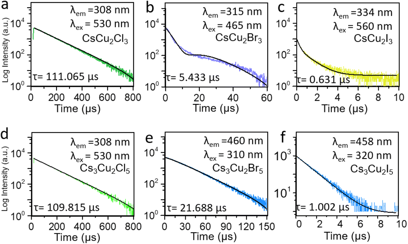 | ||
| Fig. 2 Photoluminescence decays of six lead-free perovskite (a) CsCu2Cl3 (b) Cs3Cu2Cl5 (c) CsCu2Br3 (d) Cs3Cu2Br5 (e) CsCu2I3 (f) Cs3Cu2I5 NC materials. Excitation source = EPL-405 pulsed diode laser, rep rate = 100 kHz, λem = 780 nm, Δλem = 10 nm. | ||
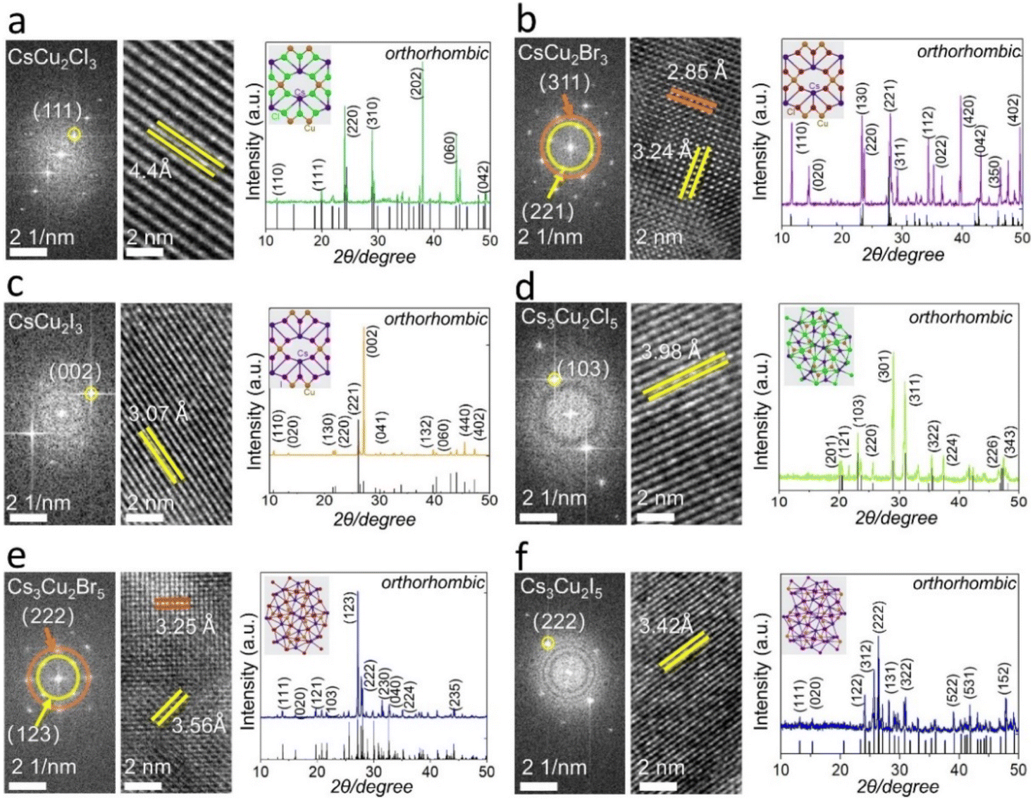 | ||
| Fig. 3 FFT images, HRTEM lattice planes, powder X-ray diffraction pattern of orthorhombic (a) CsCu2Cl3, (b) CsCu2Br3, (c) CsCu2I3, (d) Cs3Cu2Cl5, (e) Cs3Cu2Br5, and (f) Cs3Cu2I5 NC materials. The corresponding crystal systems are shown in the insets. | ||
Starting with the CsCu2Cl3 and Cs3Cu2Cl5 NC materials in Fig. 1a, it was demonstrated that the color of the PL emission (λem) systematically shifts from green (CsCu2Cl3: 530 nm) to deep green (Cs3Cu2Cl5: 495 nm), from violet (CsCu2Br3: 435 nm) to blue (Cs3Cu2Br5: 460 nm) and from yellow (CsCu2I3: 560 nm) to light green (Cs3Cu2I5: 445 nm) in Fig. 1b and c, respectively. NCs can be assigned to an orthorhombic system but different space groups, which is consistent with FFT results.14 To gain further insights into the optical properties of as-prepared PV NCs, the time-resolved PL (TRPL) and PLQYs were applied. PLQYs can be related to the defects in the materials, as one can find in Fig. 2, which demonstrates the trend in the behavior. Note, that formation of NCs was confirmed (Fig. 3) using high-resolution transmission electron microscopy (HRTEM). The PLQYs increase from 3.69% to 95.2% as substituting Cl with Br and I, opposite to the change in exciton average lifetime. The such phenomenon reflects that non-radiation losses reduce and lattice defects decrease, especially strongly for Br and I ion-containing PV materials.
The emission peaks can be further transferred into the color coordinates in Commission Internationale de L'Eclariage (CIE) 1931. The detailed parameters are summarized in Table S1 and Fig. S1.† It should be noted that CIE 1931 cites similar chromaticity coordinates for CsCu2X3 and Cs3Cu2X5 (X = Cl, Br, I) with solution-process-based PVs under 325 nm UV excitation at room temperature (RT).15
Moreover, to study the carrier dynamics of these six PV NC films on paper the TRPL measurement results (Fig. 2) were analyzed.
The average photogenerated carrier's lifetime profiles can be fitted using one or two exponential functions36
The results demonstrate that the average lifetime of these PVs synthesized using the solid-state method can be about 0.1 microsecond scale. For example, the average lifetime in CsCu2Cl3 is about 111.065 μs. However, by substituting Cl with Br and I, the average lifetime decreases to 0.631 μs. Similar behavior is obtained for Cs3Cu2X5 NC materials. It should be emphasized that the exciton lifetime of solid-state process-based NC materials is longer compared to the exciton lifetime registered in lead-free PVs synthesized using the simple solution process.31
To analyze the carrier lifetime decay of each element in these PVs, the X-ray photoelectron spectroscopy (XPS) of full spectra was further performed. The peak position of Cs 3d and I 3d had a greater shift than those of Cl 2p and Br 3d, as shown in Fig. S2–S7,† in respect to the same electron binding energies of Cu+. A similar trend is also observed for Cs3Cu2X5 single crystals, indicating the photoelectrical behavior of metal lead-free halide PVs is determined by halide ions. It should be noted that the atomic radius of Br and I atoms is larger compared to the atomic radius of Cl atom, therefore the atoms have more strong influence on carrier lifetime than Cl atom. In addition, solid-state phase lead-free metal halide PVs: CsCu2X3 and Cs3Cu2X5 NC materials exhibit higher stability in the air compared to those materials obtained using the solution phase.7,29
Furthermore, two Cu peaks of CsCu2X3 at 932.2 eV and 957.1 eV were resolved in the XPS spectra, which can be assigned to Cu 2p2/3 and Cu 2p1/2, respectively. Both Cu peaks form in [Cu2X3]1− anion sites, the [CuX3]1− is closer to the Cu+ state rather than the Cu2+ state,37 as shown in Fig. S2–S4.† However, Cu 2p2/3 and Cu 2p1/2 with a high binding energy of 931.4 eV and 958.2 eV related to the Cu 2p2/3 and Cu 2p1/2, and the Cu 2p signals in Cs3Cu2X5 NCs should be attributed to the valence of Cu+.7 Besides, the higher 933.2 and 953.7 eV, observed in Cs3Cu2X5, and the [Cu2X5]3− are closer to the Cu2+ state rather than the Cu+ state.37 This results in existing two states for the Cu 2p spectra of Cs3Cu2X5 (Fig. S5–S7†).14
Meanwhile, each PV NC material exhibits a similar XPS spectrum with the core levels of Cs 3d and Cu 2p, but different core levels of Cl 2p, Br 3d and I 3d. For example, CsCu2Cl3 exhibited a characteristic peak at ∼200 eV (Cl 2p), but no Br 3d and I 3d related peaks are observed.16 A similar tendency is also observed for Cs3Cu2X5 single crystals,21 which is in good agreement with the results of energy dispersive X-ray spectroscopy (EDS).
The element composition was subsequently confirmed by EDS, as shown in Fig. S8–S13.† All elements (Cs, Cu, Cl, Br, I) were uniformly distributed in the selected area of NC films. The corresponding atomic ratios are also evaluated, confirming the stoichiometry of the formed perovskite NC films.
The High-Resolution TEM (HRTEM) images and Fast Fourier Transform (FFT) patterns of CsCu2X3 and Cs3Cu2X5 are shown in Fig. 3. Next, the evolution of the morphology CsCu2X3 and Cs3Cu2X5 NC materials is recorded as a function of different reaction times. Images of fabricated materials were obtained after reaction time at high temperatures: 400 °C and 550 °C (only for CsCu2Br3). With gradually increasing the reaction time from 2 h to 6 h, all PV NCs became larger in size. It is worth noting that some circle- and square-shaped nanosheets of the CsCu2Cl3 and Cs3Cu2Cl5 formed (Fig. S14a–d†). On the other hand, both CsCu2Br3 NCs and Cs3Cu2Br5 NC materials are gradually connecting with each other. These processes allow forming of nanowires or micro-crosses (Fig. S14e–h†). Notably, the morphologies of CsCu2I3 do not change with a reaction time of 4 h (Fig. S15i and j†), however, nanorods can be formed after reacting for 6 h (Fig. S15e†). For the Cs3Cu2I5, the morphologies are controllable at whole reaction stages, and the NCs are uniform (Fig. S14k and l†). The final morphology after 6 h solid-phase synthesis of PVs is studied using TEM, the results are shown in Fig. S15.† The proposed solid-state phase method (at 400 °C and at 550 °C – only for CsCu2Br3 material) for the fabrication of NC materials demonstrates higher stability compared to stabilities published in literature29 with greatly reduced surface recombination rate.
To investigate the crystal phases of as-prepared perovskite NCs, powder X-ray diffraction (PXRD) was performed (Fig. 3). Each PV NC exhibited a unique PXRD pattern with distinctive characteristic peaks, confirming its crystal phase. The PXRD patterns of solid-state synthesis's Cs3Cu2X5 are in good agreement with the experiment data of Lian et al.7 The crystal structure of Cs3Cu2X5 species belongs to the space group Pnma, adopting an orthorhombic zero-dimensional structure. Besides, tetrahedral or triangular [Cu2X5]3− anion sites are isolated by cesium (Cs+) cations. For the case of CsCu2Br3 and Cs3Cu2Br5, the PXRD pattern shows orthorhombic phase with distinguished peaks: (311) and (221) in Fig. 3b, (222) and (123) in Fig. 3e, respectively. The PXRD spectrum of CsCu2X3 nanosheets does not suffer severe peak broadening, therefore this allows easier distinguishing their phase from Cs3Cu2X5 species. For instance, the one-dimensional electronic structure CsCu2X3 group belongs to the orthorhombic space group Cmcm, and the [Cu2X3]3− anion sites are also separated by rows of Cs+ cations.15 In addition, these PVs exhibit a high thermal resistance after treatment at a high temperature (400 °C or 550 °C), as well as good environmental stability after storing 60 days (Table S1†). The PXRD and XPS spectra recorded for NC PVs after two years (shown in Fig. 4) demonstrate that most of the materials have good crystallinity and reproducibility still. It should be emphasized, all PV NC powders have been stored in exposed-to-air transparent glass reagent bottles. These PVs materials have been obtained on a conductive tape of 0.3 inch discretely with PV thin-film thickness of about 2 μm. The powders stored for two years show reproducible XRD and XPS results. The fact confirms the high quality of obtained lead-free PVs.
 | ||
| Fig. 4 Powder XRD and XPS pattern obtained for different time periods: as prepared (black) and after two years (color curves): (a and b) orthorhombic CsCu2I3 and (c and d) Cs3Cu2I5; (e and f) Cs3Cu2Br5 and (g and h) Cs3Cu2Cl5 NC materials. The results demonstrate good crystallinity and stability of the PV materials. | ||
To deeply study all-inorganic lead-free PVs, flexible photodetectors based on these materials were fabricated using the paper substrate, as schematically illustrated in Fig. 5a. The copper electrodes are deposited by electron beam evaporation with a distance of 100 μm. The photodetectors exhibit obvious photoresponse at a fixed 40° angle after hundreds of bending under different wavelengths (254, 365, and 405 nm) irradiation, as shown in Fig. 5. After returning to a flat state, the optical and electrical performance can be recovered as before. The bandgap (Eg) can be subsequently evaluated by ultraviolet-visible (UV-Vis) absorption spectroscopy (Fig. S16†) and using an empirical formula Eg = hc/λ, where is the plank constant, c denotes the velocity of light, and λ is the cut-off wavelength. The Eg can be determined as 5.02 eV, 4.96 eV and 4.49 eV for CsCu2Cl3, CsCu2Br3 and CsCu2I3, 2.12 eV, 3.23 eV and 3.30 eV for Cs3Cu2Cl5, Cs3Cu2Br5 and Cs3Cu2I5 crystals, respectively. Since the valence band and conduction band are mainly formed due to the contribution of halides (Cl, Br, I) and Cu 2p orbits, respectively, and these halide and copper atoms are distributed around the hexagonal structure, therefore Cs ions have little influence on the electronic structure of band edge in the middle of the hexagonal structure.
 | ||
| Fig. 5 (a) Schematic diagram showing the device structure consisting of paper/perovskite/copper. Photocurrent output characteristics and on–off photocurrent ratio at a bias voltage of 5 mV with 10 μW cm−2 power intensities of the (b) CsCu2Cl3 (c) Cs3Cu2Cl5 (d) CsCu2Br3 (e) Cs3Cu2Br5 (f) CsCu2I3 (g) Cs3Cu2I5 film devices with various wavelengths irradiation 254, 365 and 405 nm laser intensities with (w) bent or without (w/o) bent, respectively. Insets: digital photographs of the paper-based photodetector with a channel width of 500 μm and length of 100 μm between the drain and source copper electrodes. | ||
Noteworthily, devices fabricated based on large Eg perovskites are not sensitive to 405 nm and even shorter wavelength irradiation. This can be explained as follows. The excited electrons at 254, 365 and 405 nm wavelengths irradiation could not spill over into the photon-emitting state for CsCu2I3 Eg of 4.49 eV and Cs3Cu2Br5 Eg of 3.23 eV.
To further explore the photoelectrical properties of these devices, the output characteristics and on/off current transient photoresponse of the photodetectors were recorded (Fig. 5b–g). All devices exhibit reproducible on/off cycles, indicating good electrical stability. In addition, the output photoresponse current characteristics were found to be strongly dependent upon the wavelength of the incident illumination. The fact indicates a good wavelength selectivity. The on/off ratio of the CsCu2X3 and Cs3Cu2X5 photodetectors are subsequently measured at 10 μW cm−2 and bias voltage (VDS) 5 mV, and summarized in Table 1, as a function of exciting wavelength.
| Materials | Wavelength (nm) | R (A W−1) w/o bent | R (A W−1) w bent | D* (jones) w/o bent | D* (jones) w bent |
|---|---|---|---|---|---|
| CsCu2Cl3 | 254 | 1.10 × 10⁻³ | 3.76 × 10⁻⁴ | 7.46 × 10⁹ | 2.71 × 10⁹ |
| 365 | 4.36 × 10⁻⁴ | 2.11 × 10⁻⁴ | 2.96 × 10⁹ | 1.52 × 10⁹ | |
| 405 | 3.20 × 10⁻⁴ | 1.40 × 10⁻⁴ | 2.17 × 10⁹ | 1.01 × 10⁹ | |
| Cs3Cu2Cl5 | 254 | 6.84 × 10⁻⁴ | 2.66 × 10⁻⁴ | 4.51 × 10⁹ | 1.75 × 10⁹ |
| 365 | 1.92 × 10⁻⁴ | 1.77 × 10⁻⁴ | 1.26 × 10⁹ | 1.17 × 10⁹ | |
| 405 | 1.84 × 10⁻⁴ | 2.66 × 10⁻⁴ | 1.21 × 10⁹ | 1.75 × 10⁹ | |
| CsCu2Br3 | 254 | 3.44 × 10⁻⁴ | 2.56 × 10⁻⁴ | 2.40 × 10⁹ | 1.79 × 10⁹ |
| 365 | 2.35 × 10⁻⁴ | 1.76 × 10⁻⁴ | 1.65 × 10⁹ | 1.23 × 10⁹ | |
| 405 | 1.72 × 10⁻⁴ | 1.48 × 10⁻⁴ | 1.20 × 10⁹ | 1.03 × 10⁹ | |
| Cs3Cu2Br5 | 254 | 2.96 × 10⁻⁴ | 2.64 × 10⁻⁴ | 1.59 × 10⁹ | 1.41 × 10⁹ |
| 365 | 2.88 × 10⁻⁴ | 2.56 × 10⁻⁴ | 1.54 × 10⁹ | 1.37 × 10⁹ | |
| 405 | 2.76 × 10⁻⁴ | 2.41 × 10⁻⁴ | 1.48 × 10⁹ | 1.29 × 10⁹ | |
| CsCu2I3 | 254 | 2.52 × 10⁻⁴ | 2.23 × 10⁻⁴ | 1.39 × 10⁹ | 1.23 × 10⁹ |
| 365 | 2.28 × 10⁻⁴ | 2.16 × 10⁻⁴ | 1.26 × 10⁹ | 1.20 × 10⁹ | |
| 405 | 2.20 × 10⁻⁴ | 2.12 × 10⁻⁴ | 1.22 × 10⁹ | 1.17 × 10⁹ | |
| Cs3Cu2I5 | 254 | 3.28 × 10⁻⁴ | 2.48 × 10⁻⁴ | 3.92 × 10⁹ | 2.14 × 10⁹ |
| 365 | 4.84 × 10⁻⁴ | 3.54 × 10⁻⁴ | 2.68 × 10⁹ | 1.96 × 10⁹ | |
| 405 | 7.08 × 10⁻⁴ | 3.87 × 10⁻⁴ | 1.82 × 10⁹ | 1.37 × 10⁹ |
The R and D* decreased after the bending with a bending angle of 40° and recorded in Table 1 (the bent direction is parallel to the arrow in Fig. 5b), respectively. The bending of the absorbing surface changes the incident angle and area of the light, which reduced the projected area of light on the PV photodetector. Although the on-off ratio and the response speed of the perovskite devices are far from the desired state-of-art photoelectric application, all these results indicated that the photodetectors using the solid-state method may exhibit good near ultraviolet photoresponse, as well as stable and reproducible photo-switching characteristic as it is shown in this work. It should be noted that photovoltaic properties, allowing to capture of solar energy will enable the future fabrication of wearable biosensors, which do not require a battery. The devices fabricated on the flexible substrate will enable the exploration of new pathways for delivering approaches to create highly functional skin-integrated biosensors employing photovoltaic techniques that are capable of working on renewable energy sources, reducing the cost in a green energy and technology strategy. These innovations may be quickly implemented by the industry for commercial production to bring high-speed, safe and effective biomedical devices to market more quickly and at a cost-efficient basis, to play a major role in solving global challenges in an environmentally-friendly and sustainable way.
Experimental
Materials
The following commercial materials were utilized without further purification unless otherwise indicated. CsBr (99.998%, Xi'an Polymer Light Technology Corp, China), CsBr (99.993%, Xi'an Polymer Light Technology Corp, China), CsI (99.997%, Xi'an Polymer Light Technology Corp, China), CuI (97%, Aladdin), CuBr (98%, Aladdin), CuCl (≥96%) and N,N-dimethylformamide (DMF, ≥99%, Sigma-Aldrich).Synthesis of NC materials with the solid-state method
All perovskites were prepared by reacting a 1:2, 3:2 stoichiometric ratio of CsX:CuX (X = Cl, Br, I) reactants. To ensure the homogeneity of all studied perovskite precursors, all reactants were ground in zirconia ball mill jars and then sealed in evacuated quartz ampules. Reaction mixtures were then, after the optimization, annealed at 400 °C (or 550 °C only CsCu2Br3 NC material) for 6 h (raise step is 5 °C per min from RT for 4.5 h) and natural cooling to room temperature for 5 h. As-prepared 200 mg perovskite powders (200 mg) were subsequently dissolved in a DMF (50 mL) under 200 °C heating. To fabricate a high-quality perovskite thin film, the perovskite solution was spin-coated on a paper-based substrate with a rotation speed of 1200 rpm for 35 s, followed by annealing at 100 °C for 15 min. The DMF will evaporate from PVs thin films. The Cu electrode with a thickness of 400 nm was deposited using EBV technology and then the devices with sub-micrometer characteristic size were formed.
Material characterization
The morphology of samples is analyzed using SEM (FEI NanoSEM 50). Chemical identification of perovskite NCs was conducted by XRD (MAXima XRD-7000). The micro-level structure is characterized by TEM (FEI Tecnai G2F20 S-Twin). For the elemental analysis of the as-synthesized perovskite NCs, XPS data are obtained on a Kratos AXIS-ULTRA DLD photoelectron spectrometer. UV/Vis absorption spectra are obtained using a PerkinElmer UV WinLab, spectrophotometer. PLQYs measurements were performed using HAMAMATSU Quantaurus-QY Plus UV-NIR. The fluorescence lifetime image and excitation spectra were employed for Edinburgh FLS1000 spectrofluorometer at RT. Reflection spectra were obtained by a Shimadzu UV2600 with the external integrating sphere at RT.Device characterization
The direct current characteristics I–V curves of the perovskite photodetector were carried out using an Agilent parameter analyzer B1500a. The laser diode is controlled to produce a square wave light pulse by a programmable power source Agilent E3640A.Conclusions
In summary, facile scale-up synthesis of Cs copper halide NC materials using the solid-state method developed in this work is reported. Such perovskite NCs not only exhibited a good thermal stability after storing in an air environment for two years but also high PLQYs reaching up to 90%. Moreover, a long carrier lifetime of ∼116 μs was obtained, showing a good crystal quality of synthesized NC materials. The flexible photodetectors based on these materials undoubtedly exhibited a good photoresponse to UV light, including a responsivity of above 1.0 × 10⁻⁴ A W−1, a detectivity of 1.0 × 10⁹ jones under such low photon power density (10 μW cm−2) and VDS = 5 mV. Finally, good air stability and photoswitching characteristics achieved for the photodetectors on flexible substrates show great potential for future flexible electronics, including bioelectronics and solar energy-powered biosensors on the flexible substrate.Author contributions
Zhi Jiang conceived the idea of scale-up perovskite synthesis and assembled photodetector on flexible paper. Hezhuang Liu and Jihua Zou verified the analytical methods. Yixuan Huang contributed to the interpretation of the results. Zhaoquan Xu and Denys Pustovyi carried out the experiment and contributed to the presentation of the original research data; Svetlana Vitusevich contributed to the writing and editing of the paper. All authors have read, contributed to the editing and agreed on the present version of the manuscript.Conflicts of interest
There are no conflicts to declare.Acknowledgements
Jiang Wu received funding from the National Key Research and Development Program of China (No. 2019YFB2203400), the “111 Project” (No. B20030), the UESTC Shared Research Facilities of Electromagnetic Wave and Matter Interaction (No. Y0301901290100201) and the Central Government Funds of Guiding Local Scientific and Technological Development for Sichuan Province (No. 2021ZYD0023). Zhi Jiang received funding for China Postdoctoral Science Foundation. (Award/Contract Number 2020M673179). Most of this work was financially supported from Prof. Jiang Wu as my co-advisor. Dr Kai Shen support technical guidance of this work. The authors are also grateful for the support of the Central Institute of Engineering, Electronics and Analytics (ZEA-3) at Forschungszentrum Jülich for XPS measurements.References
- K. Huang, J. X. Liu, X. J. Chang and L. Fu, Integrating Properties Modification in the Synthesis of Metal Halide Perovskites, Adv. Mater., 2018, 4, 1800321 Search PubMed.
- I. Levchuk, A. Osvet, X. Tang, M. Brandl, J. D. Perea, F. Hoegl, G. J. Matt, R. Hock, M. Batentschuk and C. J. Brabec, Brightly Luminescent and Color-Tunable Formamidinium Lead Halide Perovskite FAPbX3 (X = Cl, Br, I) Colloidal Nanocrystals, Nano Lett., 2017, 17, 2765–2770 CrossRef CAS PubMed.
- S. Govinda, B. P. Kore, D. Swain, A. Hossain, C. De, T. N. G. Row and D. D. Sarma, Critical Comparison of FAPbX3 and MAPbX3 (X = Br and Cl): How Do They Differ?, J. Phys. Chem. C, 2018, 122, 13758–13766 CrossRef CAS.
- Y. J. Dou, S. Wang, C. X. Zhang, H. D. Luo, X. M. Li, H. R. Wang, F. Cao, P. Y. Shen, J. H. Zhang and X. Y. Yang, Ten-Gram-Scale Synthesis of FAPbX3 Perovskite Nanocrystals by a High-Power Room-Temperature Ultrasonic-Assisted Strategy and Their Electroluminescence, Adv. Mater. Technol., 2020, 5, 1901089 CrossRef CAS.
- A. Jaffe, Y. Lin, C. M. Beavers, J. Voss, W. L. Mao and H. I. Karunadasa, High-Pressure Single-Crystal Structures of 3D Lead-Halide Hybrid Perovskites and Pressure Effects on their Electronic and Optical Properties, ACS Cent. Sci., 2016, 2, 201–209 CrossRef CAS PubMed.
- M.-G. Jeon, S. Yun, A. Kirakosyan, M. R. Sihn, S.-G. Yoon and J. Choi, Scale-Up Synthesis of Organometal Halide Perovskite Nanocrystals (MAPbX3, X = Cl, Br, and I), ACS Sustainable Chem. Eng., 2019, 7, 19369–19374 CrossRef CAS.
- L. Y. Lian, M. Y. Zheng, P. Zhang, Z. Zheng, K. Du, W. Lei, J. B. Gao, G. D. Niu, D. L. Zhang, T. Y. Zhai, S. Y. Jin, J. Tang, X. W. Zhang and J. B. Zhang, Photophysics in Cs3Cu2X5 (X = Cl, Br, or I): Highly Luminescent Self-Trapped Excitons from Local Structure Symmetrization, Chem. Mater., 2020, 32, 3462–3468 CrossRef CAS.
- P. F. Cheng, L. Sun, L. Feng, S. Q. Yang, Y. Yang, D. Y. Zheng, Y. Zhao, Y. B. Sang, R. L. Zhang, D. H. Wei, W. Q. Deng and K. L. Han, Colloidal Synthesis and Optical Properties of All-Inorganic Low-Dimensional Cesium Copper Halide Nanocrystals, Angew. Chem., 2019, 131, 16087–16091 CrossRef PubMed.
- I. Levchuk, A. Osvet, X. Tang, M. Brandl, J. D. Perea, F. Hoegl, G. J. Matt, R. Hock, M. Batentschuk and C. J. Brabec, Brightly Luminescent and Color-Tunaable Formamidinium Lead Halide Perovskite FAPbX3 (X = Cl, Br, I) Colloidal Nanocrystals, Nano Lett., 2017, 17, 2765–2770 CrossRef CAS PubMed.
- Y. C. Ling, Z. Yuan, Y. Tian, X. Wang, J. C. Wang, Y. Xin, K. Hanso, B. W. Ma and H. W. Gao, Bright Ligh-Emitting Diodes Based on Organometal Halide Perovskite Nanoplatelets, Adv. Mater., 2015, 28, 305–311 CrossRef PubMed.
- J. H. Noh, S. H. Im, J. H. Heo, T. N. Mandal and S. I. Seok, Chemical Management for Colorful, Efficient, and Stable Inorganic-Organic Hybrid Nanostructured Solar Cells, Nano Lett., 2013, 13, 1764–1769 CrossRef CAS PubMed.
- Z. Guo, J. Li, R. Pan, J. Cheng, R. Chen and T. He, All-inorganic copper(i)-based ternary metal halides: promising materials toward optoelectronics, Nanoscale, 2020, 12, 15560–15576 RSC.
- X. M. Li, Y. Wu, S. L. Zhang, Y. G. Bo Cai, J. Z. Song and H. B. Zeng, CsPbX3 Quantum Dots for Lighting and Displays: RoomTemperature Synthesis, Photoluminescence Superiorities, Underlying Origins and White Light-Emitting Diodes, Adv. Funct. Mater., 2016, 26, 2435–2445 CrossRef CAS.
- Y. Y. Li, P. Vashishtha, Z. C. Zhou, Z. Li, S. B. Shivarudraiah, C. Ma, J. Liu, K. S. Wong, H. B. Su and J. E. Halpert, Room Temperature Synthesis of Stable, Printable Cs3Cu2X5 (X = I, Br/I, Br, Br/Cl, Cl) Colloidal Nanocrystals with Near-Unity Quantum Yield Green Emitters (X = Cl), Chem. Mater., 2020, 32, 5515–5524 CrossRef CAS.
- R. Roccanova, A. Yangui, G. Seo, T. D. Creason, u. Wu, D. Y. Kim, M.-H. Du and B. Saparov, Bright Luminescence from Nontoxic CsCu2X3 (X = Cl, Br, I), ACS Mater. Lett., 2019, 1, 459–465 CrossRef CAS.
- Z. Zhou, Y. Li, Z. Xing, H. H. Y. Sung, I. D. Williams, Z. Li, K. S. Wong and J. E. Halpert, Rapid Synthesis of Bright, Shape-Controlled, Large Single Crystals of Cs3Cu2X5 for Phase Pure Single (X = Br, Cl) and Mixed Halides (X = Br/Cl) as the Blue and Green Components for Printable White Light-Emitting Devices, Adv. Mater. Interfaces, 2021, 8, 2101471 CrossRef CAS.
- K. M. McCall, C. C. Stoumpos, S. S. Kostina, M. G. Kanatzidis and B. W. Wessels, Strong Electron–Phonon Coupling and Self-Trapped Excitons in the Defect Halide Perovskites A3M2I9 (A = Cs, Rb; M = Bi, Sb), Chem. Mater., 2017, 29, 4129–4145 CrossRef CAS.
- A. F. Wang, Y. Y. Guo, Z. B. Zhou, X. H. Niu, Y. G. Wang, F. Muhammad, H. B. Li, T. Zhang, J. L. Wang, S. M. Nie and Z. T. Deng, Aqueous acid-based synthesis of lead-free tin halide perovskites with near-unity photoluminescence quantum efficiency, Chem. Sci., 2019, 17, 4573–4579 RSC.
- T. Yuan, F. L. Yuan, X. H. Li, Y. C. Li, L. Z. Fan and S. H. Yang, Fluorescence phosphorescence dual emissive carbon nitride quantum dots show 25% white emission efficiency enabling single-component WLEDs, Chem. Sci., 2019, 10, 9801–9806 RSC.
- H. Xu, A. B. Ren, J. Wu and Z. M. Wang, Recent Advances in 2D MXenes for Photodetection, Adv. Funct. Mater., 2020, 30, 2000907 CrossRef CAS.
- Z. Luo, Q. Li, L. Zhang, X. Wu, L. Tan, C. Zou, Y. Liu and Z. Quan, 0D Cs3Cu2X5 (X = I, Br, and Cl) Nanocrystals: Colloidal Syntheses and Optical Properties, Small, 2019, 16, 1905226 CrossRef PubMed.
- P. K. Nayak, D. T. Moore, B. Wenger, S. Nayak, A. A. Haghighirad, A. Fineberg, N. K. Noel, O. G. Reid, G. Rumbles, P. Kukura, K. A. Vincent and H. J. Snaith, Mechanism for rapid growth of organic-inorganic halide perovskite crystals, Nat. Commun., 2016, 7, 13303 CrossRef CAS PubMed.
- M. I. Saidaminov, A. L. Abdelhady, B. Murali, E. Alarousu, V. M. Burlakov, W. Peng, I. Dursun, L. F. Wang, Y. He, G. Maculan, A. Goriely, T. Wu, O. F. Mohammed and O. M. Bakr, High-quality bulk hybrid perovskite single crystals within minutes by inverse temperature crystallization, Nat. Commun., 2015, 6, 7586 CrossRef PubMed.
- T. Li, X. M. Mo, C. Y. Peng, Q. C. Lu, C. J. Qi, X. M. Tao, Y. F. Ouyang and Y. L. Zhou, Distinct green electroluminescence from lead-free CsCuBr2 halide micro-crosses, Chem. Commun., 2019, 55, 4554–4557 RSC.
- N. Sakai, A. A. Haghighirad, M. R. Filip, P. K. Nayak, S. Nayak, A. Ramadan, Z. P. Wang, F. Giustino and H. J. Snaith, Solution-Processed Cesium Hexabromopalladate(IV), Cs2PdBr6, for Optoelectronic Applications, J. Am. Chem. Soc., 2017, 139, 6030–6033 CrossRef CAS PubMed.
- D. B. Straus, S. Guo and R. J. Cava, Kinetically Stable Single Crystals of Perovskite-Phase CsPbI3, J. Am. Chem. Soc., 2019, 141, 11435–11439 CrossRef CAS PubMed.
- X. Hu, Y. Li, Y. Wu, W. Chen, H. Zeng and X. Li, One-pot synthesis of Cs3Cu2I5 nanocrystals based on thermodynamic equilibrium, Mater. Chem. Front., 2021, 5, 6152–6159 RSC.
- J. H. Han and W. B. Im, Mechanochemical Synthesis As a Green Route: Cs3Cu2X5 (X = Cl, Br, I) and CsCu2I3 and Their Reversible Phase Transitions, ECS Meeting Abstracts, 2022, MA2022-02, 1986 CrossRef.
- X. Y. Huang, Q. Sun and B. Devakumar, Facile low-temperature solid-state synthesis of efficient blue-emitting Cs3Cu2I5 powder phosphors for solid-state lighting, Mater. Today Chem., 2020, 17, 100288 CrossRef CAS.
- R. Roccanova, A. Yangui, H. Nhalil, H. L. Shi, M.-H. Du and B. Saparov, Near-Unity Photoluminescence Quantum Yield in Blue-Emitting Cs3Cu2Br5-xIx (0<x<5), ACS Appl. Electron. Mater., 2019, 1, 269–274 CrossRef CAS.
- T. Jun, K. Sim, S. Iimura, M. Sasase, H. Kamioka, J. Kim and H. Hosono, Lead-Free Highly Efficient Blue-Emitting Cs3Cu2I5 with 0D Electronic Structure, Adv. Mater., 2018, 30, 1804547 CrossRef PubMed.
- Z. X. Zhang, C. Li, Y. Lu, X. W. Tong, F. X. Liang, X. Y. Zhao, D. Wu, C. Xie and L. B. Luo, Sensitive Deep Ultraviolet Photodetector and Image Sensor Composed of Inorganic Lead-Free Cs3Cu2I5 Perovskite with Wide Bandgap, J. Phys. Chem. Lett., 2019, 10, 5343–5350 CrossRef CAS PubMed.
- D. D. Zhang, S. W. Eaton, Y. Yu, L. T. Dou and P. D. Yang, Solution-Phase Synthesis of Cesium Lead Halide Perovskite Nanowires, J. Am. Chem. Soc., 2015, 137, 9230–9233 CrossRef CAS PubMed.
- H. Jing, R. Peng, R.-M. Ma, J. He, Y. Zhou, Z. Yang, C.-Y. Li, Y. Liu, X. Guo, Y. Zhu, D. Wang, J. Su, C. Sun, W. Bao and M. Wang, Flexible Ultrathin Single-Crystalline Perovskite Photodetector, Nano Lett., 2020, 20, 7144–7151 CrossRef CAS PubMed.
- M. Zhang, Q. Lu, C. Wang, H. Dai, Y. Xue, J. He and B. Ge, Improving the performance of ultra-flexible perovskite photodetectors through cation engineering, J. Phys. D: Appl. Phys., 2020, 53, 235107 CrossRef CAS.
- R. Lin, Q. L. Guo, Q. Zhu, Y. M. Zhu, W. Zheng and F. Huang, All-Inorganic CsCu2I3 Single Crystal with High-PLQY (≈15.7%) Intrinsic White-Light Emission via Strongly Localized 1D Excitonic Recombination, Adv. Mater., 2019, 31, 1905079 CrossRef CAS PubMed.
- J. Yang, W. Kang, Z. Z. Liu, M. Y. Pi, L. B. Luo, C. Li, H. Lin, Z. T. Luo, J. Du, M. Zhou and X. S. Tang, High-Performance Deep Ultraviolet Photodetector Based on a One-Dimensional Lead-Free Halide Perovskite CsCu2I3 Film with High Stability, J. Phys. Chem. Lett., 2020, 11, 6880–6886 CrossRef CAS PubMed.
Footnote |
| † Electronic supplementary information (ESI) available. CCDC 1667477–1667479 and 1667484–1667486. For ESI and crystallographic data in CIF or other electronic format see DOI: https://doi.org/10.1039/d2ra07100b |
| This journal is © The Royal Society of Chemistry 2023 |