 Open Access Article
Excellent photocatalytic properties in 2D ZnO/SiC van der Waals hetero-bilayers: water-splitting H2-fuel production
Md. Rasidul Islam *a,
Md. Sakib Hasan Khan
 b,
Md. Rayid Hasan Mojumderbc and
Sohail Ahmadd
aDepartment of Electrical and Electronic Engineering, Bangamata Sheikh Fojilatunnesa Mujib Science & Technology University, Jamalpur-2012, Bangladesh. E-mail: rasidul@bsfmstu.ac.bd
bDepartment of Electrical and Electronic Engineering, Khulna University of Engineering & Technology, Khulna-9203, Bangladesh
cDepartment of Electrical and Electronic Engineering, Daffodil International University, Dhaka-1341, Bangladesh
dDepartment of Physics, College of Science, King Khalid University, P O Box 9004, Abha, Saudi Arabia
First published on 11th January 2023
Abstract
This research unravels the photocatalytic properties of a 2D ZnO/SiC van der Waals hetero-bilayer for potential water-splitting applications by first-principles calculations. Four unique stacking patterns are considered in studying the electronic and optical properties in the presence and absence of biaxial external strain. For pattern-I and II, large negative binding energy and positive phonon frequencies are observed, denoting chemical and mechanical stabilities. Under the HSE-06 pseudo potential, the calculated bandgap value for pattern-I and II reaches 2.86 eV and 2.74 eV, respectively. 2D ZnO/SiC shows a high absorption coefficient (∼105 cm−1). The absorption peak under biaxial strain could reach ∼3.5 times the peak observed under unstrained conditions. Under strain, a shift from compressive to tensile biaxial strain (−6% to 6%) results in a bandgap decrease from 3.18 eV to 2.52 eV and 3.09 eV to 2.43 eV, for pattern-I and II, respectively. The observed strain-driven kinetic overpotential for 2D ZnO/SiC pattern-I and II easily engenders photocatalytic redox reactions. The excellent mechanical durability and strain-driven large kinetic overpotential suggest 2D ZnO/SiC heterobilayers as a prospective material for water-splitting H2-fuel production.
1. Introduction
At present, sustainable and renewable energy alternatives are highly sought after to address the detrimental climate turmoil caused by decades of greenhouse gas emissions.1–3 Hydrogen (H2) fuel energy is thought to be one of the alternative solutions in this regard.4 However, conventional H2 fuel production, including high-temperature and pressure steam methane reforming (SMR), biomass pyrolysis, and coal gasification (∼5 MPa), emits CO2 and is inherently costly.5 Semiconductor-based photocatalytic water splitting (SPWS) provides more economical and CO2- free H2 gas.6 In SPWS, the semiconductor photocatalysts react with water and produce hydrogen (H2) and oxygen (O2) through the hydrogen evolution reaction (HER) and oxygen evolution reaction (OER), respectively. In 1972, the photocatalyst properties of TiO2 were first reported; which provoked growing attraction in this field to find novel semiconductor photocatalysts from bulk to nano.6,7 However, finding new materials that meet all the multi-facet desires of an efficient photocatalyst is still a demanding challenge.Of late, graphene and graphene-like nanostructures are widely reported for their unprecedented feasibility in efficient photocatalysis.8–10 Graphitic metal free g-C3N4 demonstrates a hydrogen yield of ∼3.2 μmol h−1 g−1 at 420 nm wavelength of photons.11 Pt co-catalyst in g-C3N4 outperforms the H2 yield by ∼35 times (∼106 μmol h−1 g−1) as in the g-C3N4.12 Bandgap-engineered graphene in the existence of a co-catalyst provides ∼1050 μmol h−1 g−1 of H2 yield.13 Prominent transition metal dichalcogenides (TMDs); MoSe2, MoS2, and WS2, synthesized experimentally, mark up ∼62![[thin space (1/6-em)]](https://www.rsc.org/images/entities/char_2009.gif) 000, ∼26
000, ∼26![[thin space (1/6-em)]](https://www.rsc.org/images/entities/char_2009.gif) 000, and ∼2570 μmol h−1 g−1 of hydrogen yield, correspondingly.14,15 Widely tailorable bandgap and peak-absorption near-visible spectrum makes InX (X = S, Se, Te) (∼2.22–3.19 eV) and GaX (X = S, Se, Te) (∼2.20–2.71 eV) as efficient photocatalysts.16 Photocatalytic activities increase in nanostructure materials due to large surface zone, higher carrier mobility, and higher reaction sites. A higher reaction rate thus follows with a larger carrier transfer. However, to make practice use of the higher reaction rate, the charge carriers are required to spatially separate externally. Technique involving vdW stacking and external biaxial strains incorporation improves carrier generations and their spatial separation. Moreover, recent investigation has demonstrated lucrative properties in vdWs structure for possible application in PWS, which encircles properties like bandgap engineering, enhanced optical absorption, in-plane and out-of-plane thermal transport, and efficient spatial carrier separation capability.17–26
000, and ∼2570 μmol h−1 g−1 of hydrogen yield, correspondingly.14,15 Widely tailorable bandgap and peak-absorption near-visible spectrum makes InX (X = S, Se, Te) (∼2.22–3.19 eV) and GaX (X = S, Se, Te) (∼2.20–2.71 eV) as efficient photocatalysts.16 Photocatalytic activities increase in nanostructure materials due to large surface zone, higher carrier mobility, and higher reaction sites. A higher reaction rate thus follows with a larger carrier transfer. However, to make practice use of the higher reaction rate, the charge carriers are required to spatially separate externally. Technique involving vdW stacking and external biaxial strains incorporation improves carrier generations and their spatial separation. Moreover, recent investigation has demonstrated lucrative properties in vdWs structure for possible application in PWS, which encircles properties like bandgap engineering, enhanced optical absorption, in-plane and out-of-plane thermal transport, and efficient spatial carrier separation capability.17–26
In recent years, a number of studies for enhancement of photocatalytic water-splitting performance cogitating broad bandgap vdWHs have been reported.27–30 Studies on vdWHs, including BP/GaN,31 ZnO/MoS2,32 GaN/GeC,33,34 ZnO/WSe2,35 blue phosphorene/g-GaN,36 graphene/g-C3N4,37 GeC/SiC,38 CdO/CdS,39 h-BN/C2N,40 ZnO/GeC,41 and blue phosphorene/MoS2,42 have demonstrated unique tunable electronic properties, improved optical absorbance, and efficient carrier separation capability, facilitating PWS. However, the optoelectronic characteristics of single-layer ZnO in its nanostructured form are still scarce though the bulk is widely studied. 2D ZnO, having high-mechanical and chemical stabilities show unique optoelectronic properties and tunability, make it a suitable candidate for PWS. Also, the stacked 2D ZnO with other 2D structures could enhance the PWS performance. 2D SiC is also another widely studied vdW stacked material that has a substantial impact on improving PWS performance. Prior 2D SiC-based device applications and their unique stability remark its potentiality for PWS.43 Generally, 2D SiC shows direct bandgap and low visible light absorption, while on stacking with other monolayers the optoelectronic properties are widely altered and enhancement in optical absorption in visible spectrum is found.44 Thus, a vdW hetero-bilayer (HBL) composed 2D ZnO and 2D SiC is expected to demonstrate excellent photocatalytic features. Nevertheless, there is absence of detailed previous study on the 2D ZnO/SiC vdWs properties for PWS application from our thoughtful. Thus ZnO/SiC vdW hetero-bilayer needs an in-depth strain-driven study to highlight the intrinsic and enhanced tunable optoelectronic photocatalytic properties.
Herein, 2D ZnO/SiC vdW HBL is widely investigated through density functional theory (DFT) for photocatalytic H2-fuel generation. Four stacked patterns of 2D ZnO/SiC vdWHs are investigated upon which two structures are underscored for excellent photocatalysis applications. The phonon dispersion is calculated to know the dynamical stability of the materials. Strain-induced electronic and optical properties of the material are also investigated and reported. Our intensive studies suggest that the 2D ZnO/SiC in its intrinsic and tuned form demonstrates promising photocatalytic performance and thus, could be considered an efficient photocatalyst for H2-fuel production.
2. Methodology
The Quantum Espresso package,45,46 norm-conserving (NC) pseudopotentials,47,48 and the Perdew–Burke–Ernzerhof (PBE)49 are employed as exchange-correlation functional to perform the density functional theory calculation. The two-atom basis unit cell of 2D ZnO and 2D SiC consists of the atoms of Zn [3d10 4s2], O [2s2 2p4], C [2s2 2p2], and Si [3s2 3p2]. The kinetic energy cut-off (charge density cut-off) was set to 400 eV (850) eV for 2D ZnO, 2D SiC, and the four stacked vdWHs. The tolerance limit of self-consistent function (SCF) was set ∼10−6 a.u. The force convergence cut-off was set to 10−3 a.u for geometry relaxation of the proposed structures. The first Brillouin zone was integrated by 8 × 8 × 1 gamma-centered Monkhorst–Pack k-mesh grid.50 A 20 Å vacuum spacing was allowed to reduce the image-layer correlation. Conventional GGA-PBE functional predicts underestimated bandgap for a semiconductor that's why Heyd–Scuseria–Ernzerhof (HSE-06) nonlocal functional was incorporated to precise prediction of the electronic gap in the band dispersion of the monolayers as well as the vdWHs.51 Along with it, vdW corrected DFT-D3 method from Grimme was applied for including the vdW interaction amid the monolayers.52Dynamical stability predicting phonon dispersions is computed by the density functional perturbation theory (DFPT) where pseudopotential as NC-PBE is used with 4 × 4 × 4 dynamical matrix.53 The optical phonon modes separation (transverse and longitudinal) was defined by the Born and Huang system.54 The complex dielectric function was employed to calculate the optical properties. The time-resolved perturbation theory in its first order was incorporated with an MP k-mesh grid of 10 × 10 × 1.55 The guiding formula of the dielectric function is ε(ω) = ε1(ω) + jε2(ω), where ε1 and ε2 are the real and the imaginary parts of the function. Adding the empty states, the imaginary part of the dielectric function is defined by,56
 | (1) |
3. Results and discussion
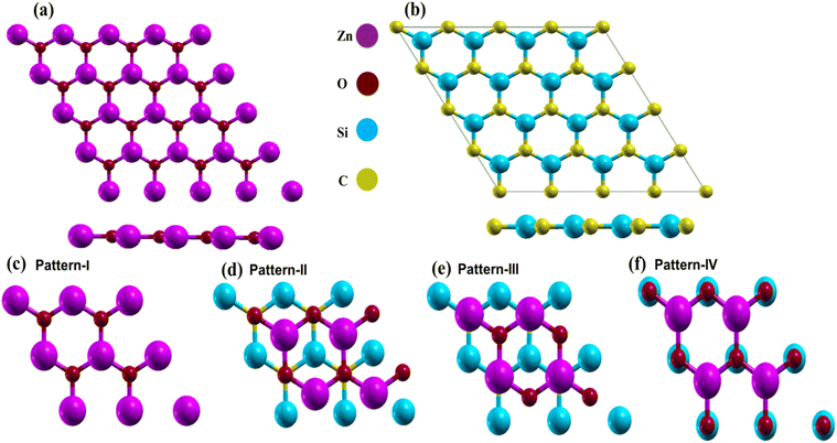
First, the structural characteristics of the proposed ZnO/SiC vdW-HBLs are investigated. The geometry relaxed 2D ZnO, SiC, and four different stacked patterns (pattern-I, II, III, and IV) are presented in Fig. 1. The intrinsic 2D ZnO, and SiC are found in non-buckling two-dimensional (2D) hexagonal structures. Here, the calculated geometry relaxed bond length of ZnO is 1.875 Å and lattice constant, a= 3.262 Å while 2D-SiC has 1.847 Å for bond length and 3.138 Å for the lattice constant. The results are closely matched with the previous studies.57,58 The four patterns were proposed by stacking a 2 × 2 2D-ZnO (a = b = 6.524 Å) layer above a 2 × 2 2D-SiC (a = b = 6.276 Å) monolayer with four unique patterns.Due to having closely matched lattice parameters of ZnO and SiC lattice disparity between ZnO and SiC layers is found around ∼3.3%, residing the maximum allowable 5% mismatch limit, calculated using the relation,  The four stacking patterns are defined as pattern I, the Zn (O) atoms of the ZnO monolayer are located right above Si (C) of the bottom SiC; pattern II(III), Zn (C) atoms were at right on top of the Si atoms, but the C (Zn) atoms were fixed at the center of the hexagons and pattern IV, the Zn and O atoms of the ZnO monolayer are on right above C and Si, correspondingly, of the bottom SiC monolayer.
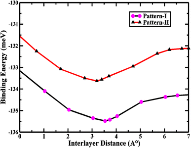
The interlayer binding energy is calculated by following the formula to predict the chemical formation probability of the stacked vdWs,
| Eb = EZnO/SiC − EZnO − ESiC | (2) |
| Pattern | a (Å) | dB (Å) | Eb (meV) | d (Å) | Eg (PBE) | Eg (HSE-06) |
|---|---|---|---|---|---|---|
| 2D-ZnO | 3.246 | 1.874 | — | — | 1.71 | 2.92 |
| 2D-SiC | 3.135 | 1.794 | — | — | 2.51 | 3.22 |
| 2D ZnO/SiC pattern-I | 3.224 | — | −135.5 | 3.54 | 1.76 | 2.86 |
| 2D ZnO/SiC pattern-II | 3.231 | — | −132.2 | 3.21 | 1.67 | 2.74 |
| 2D ZnO/SiC pattern-III | 3.234 | — | −96.8 | 3.06 | — | — |
| 2D ZnO/SiC pattern-IV | 3.226 | — | −87.6 | 3.15 | — | — |
The DFPT-based phonon dispersion predicts the dynamical stability of the projected patterns. The negative phonon frequencies found for patterns III and IV, as depicted in Fig. 3, suggest the dynamical instability of the materials. The other structures, i.e., the monolayers and pattern-I & II, having nonzero phonon frequencies show dynamical stability. The longitudinal acoustic (LA), transverse acoustic (TA), and flexural acoustic (ZA) modes are found the lowest value at the Γ point. The optical phonon modes LO and TO are found non-degenerate at Γ for the stable vdW-HBLs. The maximum frequency of the LO phonon mode is 921 cm−1 (923 cm−1) for pattern I (pattern II).
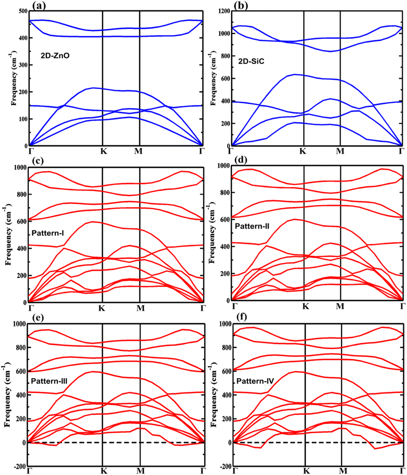 | ||
| Fig. 3 The phonon band dispersions for (a) 2D-ZnO, (b) 2D-SiC, (c) pattern-I, (d) pattern-II, (e) pattern-III, and (f) pattern-IV. | ||
Now, the electronic characteristics of 2D-ZnO, 2D-SiC, and the four stacked vdWs are calculated through DFT. The electronic dispersion at GGA-PBE and HSE-06 levels for intrinsic ZnO and SiC monolayer is calculated and demonstrated in Fig. 4, in red and blue lines, correspondingly. The calculated direct bandgap is found ∼2.92 eV and 3.234 eV at the HSE-06 level for ZnO and SiC monolayer. The bandgap and nature values of ZnO, and SiC monolayer (Fig. 4(a)) and (Fig. 4(b)) are in well-agreement with earlier studies.58,59 The band structure of the two stable vdW patterns (pattern-I, and pattern-II) are presented in Fig. 4(c) and (d), in both GGA-PBE and HSE-06 functional marked in the red and blue line, correspondingly. The ZnO monolayer has a direct bandgap at the gamma point while the SiC monolayer has a direct bandgap at K-point (Fig. 4(b)). However, both stable stacked patterns have G-point direct gap, suggesting the photocatalytic application suitability. Patterns I and II show 2.86 eV and 2.79 eV bandgap, respectively calculated using HSE-06 functional. Table 1 summarizes the different bandgap values at GGA-PBE and HSE-06 levels for the monolayers and vdWHs. To find photocatalytic kinetic overpotential, the band edge energies compared to the vacuum are needed to be calculated. Using HSE-06 bandgaps the photocatalytic band ends are formulated as,
 | (3) |
 | (4) |
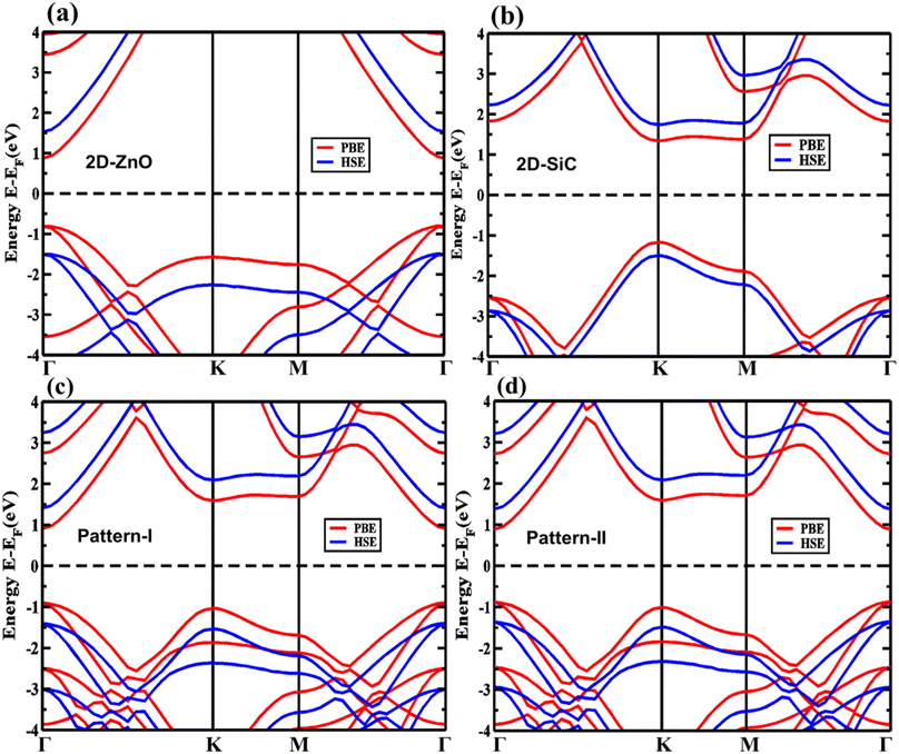 | ||
| Fig. 4 The electronic band structures for (a) ZnO monolayer, (b) SiC monolayer (2D-SiC), and for the 2D ZnO/SiC vdW HBLs (c) pattern-I, and (d) pattern-II using the PBE and HSE-06 functional. | ||
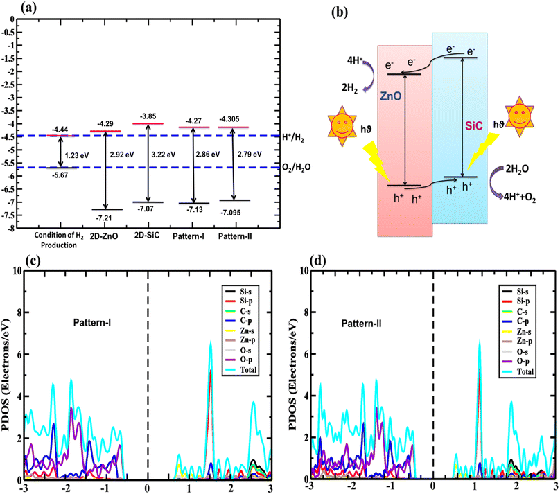
The X = Mulliken electro-negativity's geometric mean of the comprising atoms. The attained X for ZnO (SiC) monolayer is 5.75 eV (5.48 eV). The band edges for all the ZnO/SiC HBLs are also investigated for photocatalytic H2 production water-splitting capability.
Generally, semiconductors-based photocatalytic water splitting (SPWS) requires certain conditions to be met up:34 (i) the conduction band end energy level (CBE) needs to be higher or same as −4.44 eV (reduction potential) for HER (H+/H2), (ii) the valence band end (VBE) energy level needs to be lower or same as −5.67 eV (oxidation potential) for OER (O2/H2O), (iii) at least ∼1.23 eV of the bandgap is needed for the semiconductor, (iv) the semiconductor needs to possesses high-absorption in near ultra-violet (NUV), and visible spectrum, and (v) to promote H2 formation, the semiconductor must have high surface area for redox reaction.
The calculated band edges of ZnO, SiC, and ZnO/SiC vdW-HBLs are presented in Fig. 5(a). Also, the vdW HBLs show type-II bandgap as calculated in band-edges. In the monolayers and vdWHs, the conduction (valence) band edge is found greater (lower) than the potential of oxidation (reduction). Hence, the structures having adequate kinetic overpotential are promising for PWS. Additionally, the measured valence band offset (0.402 eV) and conduction band offset (0.015 eV) value is confirmed, showing carrier parting spatially. The concise carrier separation mechanism through the photo redox process is demonstrated in Fig. 5(b). The formation of the type-II bandgap is confirmed as the VBM and CBM of the SiC monolayer are below that of the ZnO monolayer. This results in the photogenerated electrons moving from ZnO to SiC monolayer strikes, surpassing conduction offset and contributing to HER to generate H2. Likely, the holes are moving toward ZnO from SiC and contribute to OER to form O2 as depicted in Fig. 5(b). Among the two stable patterns, pattern-I is shown to be the most suited photocatalyst due to having a high band offset in redox potential. From the computed total and partial density of state (DOS) to show orbital contribution in total DOS as found in Fig. 5(c) and (d), in pattern I and II, the Zn-s-orbital contributes mainly to CBM while the VBM is primarily from O-s-orbital from ZnO monolayer. Thus both of them show a type-II bandgap.
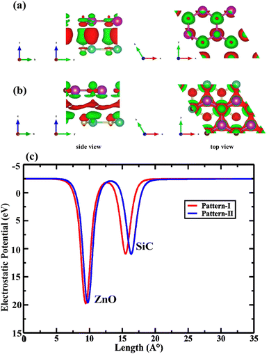
The charge sweeping between the ZnO and SiC monolayers, the charge density difference (CDD) is calculated and presented in Fig. 6 for the two patterns, as formulated, ΔρCDD = ρHBL − ρZnO − ρSiC; where, ΔρCDD is the CDD; ρHBL, ρZnO, and ρSiC, mention the charge density (CD) of the studied HBL pattern, the ZnO monolayer, and the SiC monolayer. The charge addition is marked in blue, while charge depletion is marked in red. In both pattern-I (Fig. 6(a)) and pattern-II (Fig. 6(b)), the charge lessens from the Zn atoms and collects near the O atoms of the ZnO layer. A small quantity of charge also decreases near the C atoms of the SiC layer. Interestingly, the charges are accumulated in the ZnO monolayer in all the patterns, indicating that ZnO largely determines the properties of the heterobilayer. Moreover, the most electron transport is afforded by the ZnO layer, resulting in altering bandgaps for the heterobilayer while the SiC monolayer turns into a property tuner of the heterobilayers. In Fig. 6(c), the electrostatic potential for pattern-I and pattern-II is provided, which helps to predict the charge polarities near the active sites of the monolayer surfaces. For each pattern, two negative electrostatic potential peaks are observed, one from the ZnO layer and one from the SiC layer. Electrostatic potential in ZnO being more negative refers that more electron appears on the ZnO layer; this could be due to the charge shift from the SiC layer to the ZnO layer. The potential difference between the two vertically stacked monolayer surfaces (ZnO and SiC) is 0.883 eV and 0.866 eV, respectively, for pattern-I and pattern-II. Thus, ∼0.9 eV of energy would suffice for an efficient charge transfer between the vertical layers. Fig. 7 demonstrates the electron localization function across the ZnO/SiC heterobilayer pattern-I and pattern-II atoms. It is observed that comparatively higher localization appears in the proximity of oxygen (O) and carbon (C) atoms of the ZnO and SiC layer. The inherent electron affinity of O and C could be a crucial factor that pulls the localized σ-bonds’ electrons formed through the covalent sp3 bonding of SiC and ZnO.
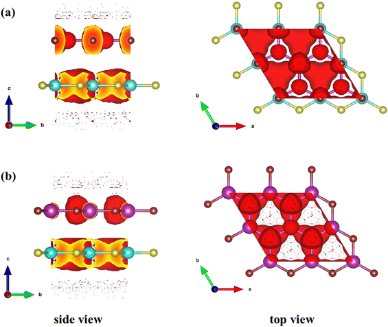 | ||
| Fig. 7 Electron localization function of (a) pattern-I and (b) pattern-II of 2D ZnO/SiC heterobilayer structure. The red overlayer refers to the localized electron. | ||
Altering electronic properties of the vdWHs, biaxial strain is a significant way. Therefore, the biaxial strain-induced electronic property is investigated. Here, the 2% incremental −6% to +6% strain range is considered. In Fig. 8(a) the strain-tuned bandgaps are shown. It is clear that a noticeable lowering of the bandgap is found from compressive to tensile strain application due to CBM and VBM moving on the Fermi level. This trend is found in both the PBE and HSE-06 levels of the bandgap values. This bandgap lowering facilitates high absorption in the visible spectrum due to the shifting of absorption peaks from UV to the visible spectrum, suitable for photocatalytic application. As strains tune the bandgap, the photocatalytic band edges are also calculated for strain-tuned bandgap value as seen in Fig. 8(b) and (c) for pattern-I and II. In the whole strain range, pattern-I has sufficient kinetic overpotential while pattern II has sufficient kinetic overpotential except at 6% tensile strain. These findings suggest that the proposed vdWHs, with a tunable photocatalytic feature, can be a potential candidate for PWS.
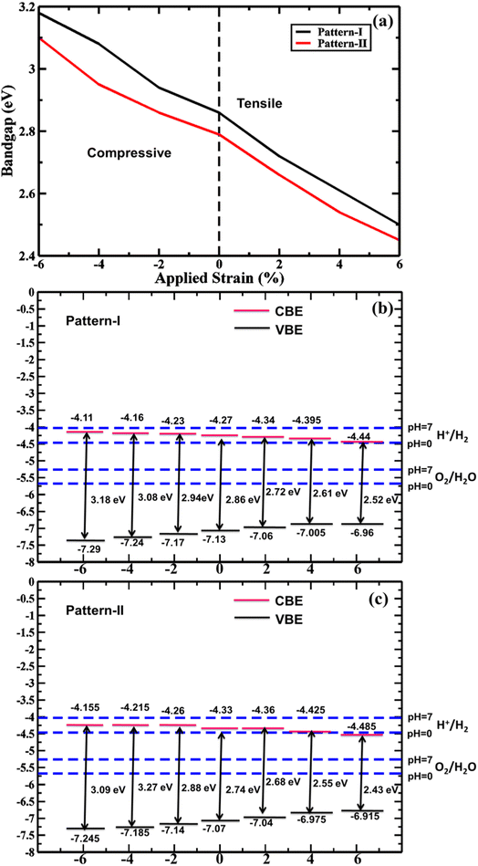 | ||
| Fig. 8 Strain-dependent (a) bandgap and band edge position for (b) pattern-I and (c) pattern-II 2D ZnO/SiC vdW HBLs using the HSE-06 functional. | ||
To study the optical features of the stable vdWHs, the first-order DFPT is incorporated. The real and the imaginary parts, signifying the result of scattering and absorption are obtained through Kramers–Kronig conversion, and momentum matrix, correspondingly. The dielectric function defined by ε(ω) = ε1(ω) + iε2(ω), with angular frequency (ω) strikes it. While the absorption coefficient of the materials can be formulated by real and imaginary dielectric functions portions as,
 | (5) |
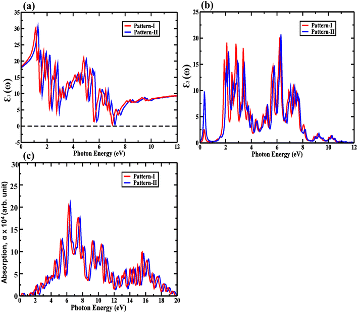 | ||
| Fig. 9 (a) The real, (b) imaginary parts of the dielectric function, and (c) absorption for pattern-I and pattern-II of 2D ZnO/SiC vdW HBLs. | ||
Our proposed ZnO/SiC HBLs show an enhanced absorption peak as demonstrated in Fig. 9. The peak absorption is acquired ∼3.9 × 105 cm−1, and 4 × 105 cm−1, at 6.4 eV, and 6.5 eV, suitable for photocatalytic application.45 A large number of absorption peaks and high-intensity peaks mean high absorption, resulting in a more photo-generated carrier, a requirement for photocatalyst. Apart from this, a larger number of peaks, inferring, more carrier transition, predict high mobility of carrier. Furthermore, the visible peak is at (∼3.4 eV) of ∼1 × 105 cm−1 in the visible spectrum.
Introducing biaxial strain can shift the absorption peaks from UV to visible and render efficient utilization of solar spectra. Biaxial strain-induced optical absorption is thus investigated as exposed in Fig. 10 (a) and (b) for −6% to +6% biaxial strains. The absorption top-points are at ∼410 nm, and ∼415 nm, wavelength for pattern-I, and II, similarly, and outcome an absorption coefficient of ∼7 × 105 cm−1, and ∼7.2 × 105 cm−1. Yet, compressive strains shift the absorption peak from UV to visible. Additionally, pattern-II shows the highest tuned due to applied biaxial strains. Moreover, a significant portion of the optical absorption coefficient is near the UV region, suggesting enhanced optical performance. The biaxial strained tuned low-bandgap values are also responsible for the high-absorption peaks near UV. These two effects get combined, resulting in efficiently utilized solar spectra by the proposed HBLs.
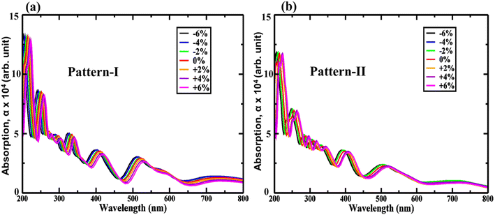 | ||
| Fig. 10 Strain-induced absorption properties for (a) pattern-I and (b) pattern-II of 2D ZnO/SiC vdW HBLs. | ||
4. Conclusions
In this report, the novel 2D ZnO/SiC vdWHs by dint of first-principles density functional theory are thoroughly studied. Phonon dispersions and binding energy of ZnO/SiC show dynamic stability and chemical formidability. Stacked patterns have direct bandgaps of 2.86 eV for pattern-I and 2.74 eV for pattern-II as obtained with the HSE-06. Biaxial strain tailored the bandgap, and the edges and initiate UV to visible shifting, through bandgap lowering, resulting in a high photogenerated carrier for photocatalysis. The bandgap-lowering nature is monotonic from compressive to tensile strains. The intrinsic optical absorption peak is achieved at ∼105 cm−1 comparable with efficient optoelectronic materials. Biaxial strains introduce the enhancement of optical absorption and UV to visible shifting, facilitating the photocatalytic activity. Concisely, the findings we have obtained for SiC/ZnO vdWHs are indicative of the potential application of this material in efficient photocatalytic water-splitting technology.Conflicts of interest
There are no conflicts to declare.Acknowledgements
Sohail Ahmad extends his appreciation to the Deanship of Scientific Research at King Khalid University for financial support through the general research program under grant number GRP-172-43.References
- S. Chu and A. Majumdar, Nature, 2012, 488, 294–303 CrossRef CAS PubMed.
- E. Serrano, G. Rus and J. García-Martínez, Renewable Sustainable Energy Rev., 2009, 13, 2373–2384 CrossRef CAS.
- M. Zäch, C. Hägglund, D. Chakarov and B. Kasemo, Curr. Opin. Solid State Mater. Sci., 2006, 10, 132–143 CrossRef.
- C. Liu, U. Burghaus, F. Besenbacher and Z. L. Wang, ACS Nano, 2010, 4, 5517–5526 CrossRef CAS PubMed.
- A. P. Simpson and A. E. Lutz, Int. J. Hydrogen Energy, 2007, 32, 4811–4820 CrossRef CAS.
- G. L. Chiarello, M. H. Aguirre and E. Selli, J. Catal., 2010, 273, 182–190 CrossRef CAS.
- M. M. Momeni and Y. Ghayeb, J. Alloys Compd., 2015, 637, 393–400 CrossRef CAS.
- Q. Xiang, J. Yu and M. Jaroniec, Chem. Soc. Rev., 2012, 41, 782–796 RSC.
- C. Han, N. Zhang and Y.-J. Xu, Nano Today, 2016, 11, 351–372 CrossRef CAS.
- Md. R. Islam, K. Liu, Z. Wang, S. Qu, C. Zhao, X. Wang and Z. Wang, Chem. Phys., 2021, 542, 111054 CrossRef CAS.
- A. Di Bartolomeo, Nanomaterials, 2020, 10, 579 CrossRef CAS PubMed.
- J. Ran, W. Guo, H. Wang, B. Zhu, J. Yu and S.-Z. Qiao, Adv. Mater., 2018, 30, 1800128 CrossRef PubMed.
- A. K. Singh, K. Mathew, H. L. Zhuang and R. G. Hennig, J. Phys. Chem. Lett., 2015, 6, 1087–1098 CrossRef CAS PubMed.
- B. Amin, N. Singh and U. Schwingenschlögl, Phys. Rev. B: Condens. Matter Mater. Phys., 2015, 92, 075439 CrossRef.
- Q. Lu, Y. Yu, Q. Ma, B. Chen and H. Zhang, Adv. Mater., 2016, 28, 1917–1933 CrossRef CAS PubMed.
- H. L. Zhuang and R. G. Hennig, Chem. Mater., 2013, 25, 3232–3238 CrossRef CAS.
- A. Rawat, R. Ahammed, D. Dimple, N. Jena, M. K. Mohanta and A. De Sarkar, J. Phys. Chem. C, 2019, 123, 12666–12675 CrossRef CAS.
- M. R. H. Mojumder, M. S. Islam and J. Park, AIP Adv., 2021, 11, 015126 CrossRef CAS.
- N. Ferdous, Md. S. Islam, J. Park and A. Hashimoto, AIP Adv., 2019, 9, 025120 CrossRef.
- A. S. Rashid, Md. S. Islam, N. Ferdous, K. N. Anindya, J. Park and A. Hashimoto, J. Comput. Electron., 2019, 18, 836–845 CrossRef CAS.
- Md. S. Islam, Md. R. H. Mojumder, N. Ferdous and J. Park, Mater. Today Commun., 2021, 26, 101718 CrossRef CAS.
- Md. R. H. Mojumder, Md. S. Islam, Md. S. Hassan and Md. J. S. Hossain, in 2020 11th International Conference on Electrical and Computer Engineering (ICECE), 2020, pp. 141–144 Search PubMed.
- J. D. Sarker, M. S. Islam, N. Ferdous, P. P. Sarker, A. G. Bhuiyan, T. Makino and A. Hashimoto, Jpn. J. Appl. Phys., 2019, 59, SCCC03 CrossRef.
- M. S. Islam, I. Mia, S. Ahammed, C. Stampfl and J. Park, Sci. Rep., 2020, 10, 22050 CrossRef CAS PubMed.
- S. Ahammed, M. S. Islam, I. Mia and J. Park, Nanotechnology, 2020, 31, 505702 CrossRef CAS PubMed.
- M. S. Islam, M. Y. Zamil, M. R. H. Mojumder, C. Stampfl and J. Park, Sci. Rep., 2021, 11, 18669 CrossRef CAS PubMed.
- K. Ren, Y. Luo, S. Wang, J.-P. Chou, J. Yu, W. Tang and M. Sun, ACS Omega, 2019, 4, 21689–21697 CrossRef CAS PubMed.
- X. Gao, Y. Shen, Y. Ma, S. Wu and Z. Zhou, Appl. Phys. Lett., 2019, 114, 093902 CrossRef.
- X. Gao, Y. Shen, Y. Ma, S. Wu and Z. Zhou, J. Mater. Chem. C, 2019, 7, 4791–4799 RSC.
- L. Ju, Y. Dai, W. Wei, M. Li and B. Huang, Appl. Surf. Sci., 2018, 434, 365–374 CrossRef CAS.
- M. K. Mohanta, A. Rawat, D. Dimple, N. Jena, R. Ahammed and A. D. Sarkar, Nanoscale, 2019, 11, 21880–21890 RSC.
- E. Benavente, F. Durán, C. Sotomayor-Torres and G. González, J. Phys. Chem. Solids, 2018, 113, 119–124 CrossRef CAS.
- P. T. Huong, M. Idrees, B. Amin, N. N. Hieu, H. V. Phuc, L. T. Hoa and C. V. Nguyen, RSC Adv., 2020, 10, 24127–24133 RSC.
- Md. S. H. Khan, Md. R. Islam, M. S. Islam, I. M. Mehedi and Md. T. Hasan, IEEE Access, 2020, 8, 209030–209042 Search PubMed.
- F. Hu, L. Tao, H. Ye, X. Li and X. Chen, J. Mater. Chem. C, 2019, 7, 7104–7113 RSC.
- K. Ren, S. Wang, Y. Luo, Y. Xu, M. Sun, J. Yu and W. Tang, RSC Adv., 2019, 9, 4816–4823 RSC.
- F. Li, M. Tang, T. Li, L. Zhang and C. Hu, Appl. Catal., B, 2020, 268, 118397 CrossRef CAS.
- M. R. Islam, M. S. Islam, A. F. Mitul, M. R. H. Mojumder, A. S. M. J. Islam, C. Stampfl and J. Park, Sci. Rep., 2021, 11, 17739 CrossRef CAS PubMed.
- G. Wang, L. Gong, Z. Li, B. Wang, W. Zhang, B. Yuan, T. Zhou, X. Long and A. Kuang, Phys. Chem. Chem. Phys., 2020, 22, 9587–9592 RSC.
- G. Wang, Z. Li, W. Wu, H. Guo, C. Chen, H. Yuan and S. A. Yang, Phys. Chem. Chem. Phys., 2020, 22, 24446–24454 RSC.
- G. Wang, L. Zhang, Y. Li, W. Zhao, A. Kuang, Y. Li, L. Xia, Y. Li and S. Xiao, J. Phys. D: Appl. Phys., 2019, 53, 015104 CrossRef.
- M. Farbod, R. Taheri and A. Kosarian, Mater. Sci. Semicond. Process., 2021, 123, 105562 CrossRef CAS.
- R. Pandey, M. Rérat, C. Darrigan and M. Causà, J. Appl. Phys., 2000, 88, 6462–6466 CrossRef CAS.
- J. B. Casady and R. W. Johnson, Solid-State Electron., 1996, 39, 1409–1422 CrossRef.
- P. Giannozzi, O. Baseggio, P. Bonfà, D. Brunato, R. Car, I. Carnimeo, C. Cavazzoni, S. de Gironcoli, P. Delugas, F. Ferrari Ruffino, A. Ferretti, N. Marzari, I. Timrov, A. Urru and S. Baroni, J. Chem. Phys., 2020, 152, 154105 CrossRef CAS PubMed.
- P. Giannozzi, S. Baroni, N. Bonini, M. Calandra, R. Car, C. Cavazzoni, D. Ceresoli, G. L. Chiarotti, M. Cococcioni, I. Dabo, A. D. Corso, S. de Gironcoli, S. Fabris, G. Fratesi, R. Gebauer, U. Gerstmann, C. Gougoussis, A. Kokalj, M. Lazzeri, L. Martin-Samos, N. Marzari, F. Mauri, R. Mazzarello, S. Paolini, A. Pasquarello, L. Paulatto, C. Sbraccia, S. Scandolo, G. Sclauzero, A. P. Seitsonen, A. Smogunov, P. Umari and R. M. Wentzcovitch, J. Phys.: Condens. Matter, 2009, 21, 395502 CrossRef PubMed.
- G. Kresse and J. Hafner, J. Phys.: Condens. Matter, 1994, 6, 8245–8257 CrossRef CAS.
- D. R. Hamann, M. Schlüter and C. Chiang, Phys. Rev. Lett., 1979, 43, 1494–1497 CrossRef CAS.
- L. Z. Tan, A. M. Rappe and J. Yang, Phys. Rev. B, 2018, 97, 085130 CrossRef.
- H. J. Monkhorst and J. D. Pack, Phys. Rev. B: Solid State, 1976, 13, 5188–5192 CrossRef.
- J. Heyd, G. E. Scuseria, R. L. Martin and J. E. Peralta, Phys. Rev. B: Condens. Matter Mater. Phys., 2006, 74, 073101 CrossRef.
- E. Caldeweyher, C. Bannwarth and S. Grimme, J. Chem. Phys., 2017, 147, 034112 CrossRef PubMed.
- S. Baroni, S. de Gironcoli, A. Dal Corso and P. Giannozzi, Rev. Mod. Phys., 2001, 73, 515–562 CrossRef CAS.
- R. Baer, D. J. Kouri, M. Baer and D. K. Hoffman, J. Chem. Phys., 2003, 119, 6998–7002 CrossRef CAS.
- C. L. Hammer and T. A. Weber, J. Math. Phys., 1965, 6, 1591–1606 CrossRef.
- C. N. Singh, G. Pilania, J. Bárta, B. P. Uberuaga and X.-Y. Liu, J. Mater. Chem. C, 2021, 9, 7292–7301 RSC.
- A. Benzair, B. Bouhafs, B. Khelifa, C. Mathieu and H. Aourag, Phys. Lett. A, 2001, 282, 299–308 CrossRef CAS.
- Z. Xu, Y. Li, C. Li and Z. Liu, Appl. Surf. Sci., 2016, 367, 19–25 CrossRef CAS.
- Md. R. Islam, Md. S. Islam, N. Ferdous, K. N. Anindya and A. Hashimoto, J. Comput. Electron., 2019, 18, 407–414 CrossRef CAS.
| This journal is © The Royal Society of Chemistry 2023 |

