 Open Access Article
The influences of AlGaN barrier epitaxy in multiple quantum wells on the optoelectrical properties of AlGaN-based deep ultra-violet light-emitting diodes†
Tien-Yu Wanga,
Wei-Chih Lai *ab,
Qiao-Ju Xiea,
Shun-Hao Yanga,
Sheng-Po Chang
 abc,
Cheng-Huang Kuod and
Jinn-Kong Sheu
 ab
ab
aDepartment of Photonics, National Cheng Kung University, Tainan 70101, Taiwan. E-mail: weilai@ncku.edu.tw
bAdvanced Optoelectronic Technology Center, Research Center for Energy Technology and Strategy, National Cheng Kung University, Tainan 70101, Taiwan
cInstitute of Microelectronics and Department of Electrical Engineering, National Cheng Kung University, Tainan 70101, Taiwan
dInstitute of Lighting and Energy Photonics, College of Photonics, National Yang Ming Chiao Tung University, Tainan 71150, Taiwan
First published on 13th February 2023
Abstract
The growth conditions of the AlGaN barrier in AlGaN/AlGaN deep ultra-violet (DUV) multiple quantum wells (MQWs) have crucial influences on the light output power of DUV light-emitting diodes (LEDs). The reduction of the AlGaN barrier growth rate improved the qualities of AlGaN/AlGaN MQWs, such as surface roughness and defects. The light output power enhancement could reach 83% when the AlGaN barrier growth rate was reduced from 900 nm h−1 to 200 nm h−1. In addition to the light output power enhancement, lowering the AlGaN barrier growth rate altered the far-field emission patterns of the DUV LEDs and increased the degree of polarization in the DUV LEDs. The enhanced transverse electric polarized emission indicates that the strain in AlGaN/AlGaN MQWs was modified by lowering the AlGaN barrier growth rate.
1. Introduction
Deep ultraviolet (DUV) light has shown its importance in many fields, such as water purification, UV photolithography, high-density optical data storage, and portable chemical/biological agent detection/analysis systems.1–5 Furthermore, UV communication has been presented as a promising candidate for military wireless communication.6,7 A record-breaking data rate has been reported continuously in the past few years.8–11 Many applications require the light output power of the UV light source to be as high as possible. Especially, the output power of the UV light source essentially determines the transmission distance of UV communication, and its bandwidth has a major impact on the data rate.12 The light output efficiency of AlGaN-based DUV light-emitting diodes (LEDs) has been improved by the optimization of the epitaxy techniques for improving the material quality of AlN.13–17 Although the efficiency of DUV LEDs has been greatly improved, their performance is still hindered by high defect density, poor carrier injection, and low carrier confinement. Many studies have reported strategies of defect reduction via substrate or template,18–20 methods of high carrier confinement, and hole injection.21–35 Low light extraction efficiency (LEE) is another challenge in achieving high efficiency for DUV LEDs. The LEE of the DUV LEDs has been improved by utilizing the flip-chip design,36,37 a patterned sapphire substrate,20,38 a patterned p-type layer,39 and the nanowire structure.40,41AlGaN/AlGaN multiple quantum wells (MQWs) are the main active layers in DUV LEDs. The quality of AlGaN/AlGaN MQWs dominated the optoelectrical characteristics of DUV LEDs, such as leakage current and light output power. Furthermore, the defect reduction of AlGaN/AlGaN MQWs would improve the internal quantum efficiency (IQE) of DUV LEDs. The growth conditions of epitaxy directly affect the quality of AlGaN/AlGaN MQWs. Previously, Bryan et al.42 reported that the growth condition of the V/III ratio could impact the IQE of AlGaN/AlGaN MQWs. (The V/III ratio in metalorganic chemical vapor deposition (MOCVD) is normally defined as the ratio of the molar flow rate of ammonia (NH3) to the total molar flow rates of trimethylgallium (TMGa) and trimethylaluminum (TMAl).) They found that AlGaN/AlGaN MQWs grown with high V/III ratio could achieve a high IQE of ∼80%. The same group also reported that surface kinetics influence the growth of AlGaN in terms of Al composition inhomogeneity and crystal quality.43 Therefore, the growth conditions are crucial during the growth of AlGaN/AlGaN MQWs. During the growth of AlGaN/AlGaN MQWs, the condition of Al0.7Ga0.3N barrier might strongly affect the growth of the following Al0.4Ga0.6N wells. In this study, we varied the growth rates of the Al0.7Ga0.3N barrier to investigate the influences on the electrical and optical properties of DUV LEDs.
2. Experimental
Epitaxial wafers were prepared on a 2-in (0001) sapphire substrate by MOCVD (Thomas Swan close-coupled showerhead 31 × 2 in). The source materials of gallium (Ga), aluminum (Al), and nitrogen (N) were TMGa, TMAl, and NH3, respectively. The n-type doping source was silane (SiH4), and the p-type doping source was bis(cyclopentadienyl)magnesium(II) (Cp2Mg). Initially a 20 nm-thick AlN nucleation layer was deposited on sapphire at 500 °C, and a 3 μm-thick undoped AlN layer was grown at 1250 °C. The screw and edge dislocation densities of the AlN epitaxy were 1.03 × 108 cm−2 and 1.64 × 109 cm−2, respectively. Following the AlN layer, a 20-pair AlN (2.5 nm)/Al0.8Ga0.2N (2.5 nm) superlattice and a 0.5 μm-thick Al0.68Ga0.32N layer were grown as transition layers. A 1.5 μm-thick Al0.6Ga0.4N:Si layer was grown as an n-type layer. The active layer was a five-pair Al0.7Ga0.3N:Si (12 nm)/Al0.4Ga0.6N (2 nm) MQWs structure grown at 1050 °C, and a 2 nm-thick undoped Al0.65Ga0.35N was grown as the last barrier. The Al0.7Ga0.3N barriers grown at different growth rates were obtained by modifying the molar flows of TMGa and TMAl, and the molar flow of silane was also adjusted to fix the doping concentration. The growth rates of the Al0.7Ga0.3N barriers were 900, 400, and 200 nm h−1, respectively. After the MQW structure, an electron blocking layer, Al0.8Ga0.2N (7 nm), and three-pair Al0.8GaN0.2:Mg (7.5 nm)/Al0.7Ga0.3N:Mg (3.5 nm) were grown. The p-type layer consisted of a 10-pair Al0.8Ga0.2N:Mg (1 nm)/Al0.48Ga0.52N:Mg (1 nm) superlattice, a 20 nm-thick Al-grading AlGaN:Mg layer (Al composition from 47% to 25%), and 10 nm-thick GaN:Mg layer.The chip processes were performed to fabricate 500 μm × 500 μm flip-chip DUV LEDs. The mesa area was revealed by the inductively coupled plasma (ICP) etching process, and Ti (20 nm)/Al (120 nm)/Ti (100 nm)/Au (50 nm) was subsequently deposited as the n-contact. Indium tin oxide (20 nm)/Al (100 nm) was deposited on the p-GaN as the p-contact. Through the thinning and dicing processes, the DUV LED chip was flipped and mounted on the AlN submount by AuSn eutectic bonding. The epitaxial structure and the schematic of the flip-chip DUV LED are shown in Fig. S1(a) and (b) in ESI,† respectively. A Keysight B1500 semiconductor parameter analyzer was employed to measure the current–voltage (I–V) characteristics of the flip-chip DUV LEDs for high- and low-current measurements. A calibrated integrating sphere and a spectrometer (Ocean Optics USB2000) were used to measure the output power and the emission spectra at room temperature. Moreover, the surface morphology of the AlGaN/AlGaN MQWs was measured by atomic force microscopy (AFM, Bruker Dimension Icon).
3. Results and discussion
The fabricated DUV LEDs with AlGaN barrier grown at 900, 400, and 200 nm h−1 are denoted as BG900, BG400, and BG200, respectively. Fig. 1 reveals the forward I–V characteristics and dynamic resistances of the AlGaN-based DUV LEDs with different barrier growth rates. BG900, BG400, and BG200 have forward voltages (Vf) of 5.994, 5.915, and 5.948 V at 100 mA, respectively. The Vf of the DUV LEDs decreased slightly after the decrease of the AlGaN barrier growth rate. In addition, the dynamic resistances at 350 mA of DUV LEDs with different AlGaN barrier growth rates were in the range of 19.6–19.8 Ω. The inset of Fig. 1 shows the reverse I–V curves of the DUV LEDs, and the reverse leakage currents at −15 V of BG900, BG400, and BG200 were −0.2, −1.15, and −2.49 μA, respectively. The reverse leakage current at −15 V increased with the decreasing AlGaN barrier growth rate. By reducing the AlGaN barrier growth rate, the forward I–V changed slightly, but the reverse leakage current increased. The cause of the increased reverse currents of DUV LEDs with low AlGaN barrier growth rates remains unclear.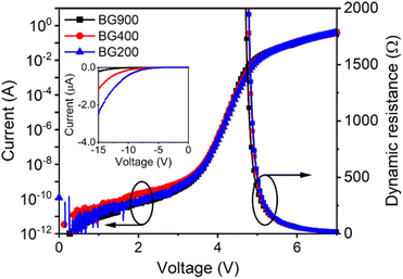 | ||
| Fig. 1 Semi-log forward I–V curves of the DUV LEDs varying AlGaN barrier growth rate. The inset of figure is linear reverse I–V curves. | ||
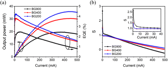
The light output power–current (L–I) and external quantum efficiency–current (EQE–I) curves of the DUV LEDs with different AlGaN barrier growth rates are presented in Fig. 2(a). The light output powers of all the DUV LEDs increased initially with the current and then reached the maximum output power at certain currents. The light output powers and EQEs of the DUV LEDs increased with decreasing AlGaN barrier growth rate for all the driving currents. The 100 mA light output powers of BG900, BG400, and BG200 were 10.01, 14.01, and 15.51 mW, and the corresponding EQEs were 2.26%, 3.16%, and 3.49%, respectively. The 100 mA light output power enhancement was 40% by reducing the barrier growth rate from 900 nm h−1 to 400 nm h−1, and the 100 mA light output enhancement could reach the largest value of 55% when the barrier growth rate was reduced to 200 nm h−1. The enhancements of the maximum light output power were 55% and 83% for the barrier growth rates of 400 and 200 nm h−1, respectively, compared with the barrier growth rate of 900 nm h−1. The driving currents for the maximum light output power increased with the decrease of the barrier growth rate. The peak EQEs of BG900, BG400, and BG200 were 2.48%, 3.87%, and 4.27%, respectively. The corresponding improvements of EQE were 56% and 73% for the reductions of the barrier growth rates from 900 nm h−1 to 400 and 200 nm h−1, respectively. Furthermore, the efficiency droops (defined as 1 − EQE450mA/EQEpeak) of the DUV LEDs were improved by decreasing the barrier growth rate. The efficiency droops of BG900, BG400, and BG200 were 62%, 57%, and 58%, respectively. The enhancements of the light output power and EQE of the DUV LEDs could be attributed to the quality improvement of the low AlGaN barrier growth rate.
The L–I curves were further analysed by dlog![[thin space (1/6-em)]](https://www.rsc.org/images/entities/char_2009.gif) L/dlog
L/dlog![[thin space (1/6-em)]](https://www.rsc.org/images/entities/char_2009.gif) I (ref. 44) (S is defined as the differential of the log
I (ref. 44) (S is defined as the differential of the log![[thin space (1/6-em)]](https://www.rsc.org/images/entities/char_2009.gif) L–log
L–log![[thin space (1/6-em)]](https://www.rsc.org/images/entities/char_2009.gif) I curve) to obtain the S–I curves to further elucidate the dominant carrier recombination process in the DUV LEDs with different AlGaN barrier growth rates. BG400 and BG200 presented lower S values than BG900 in the low injection current region (<40 mA), as presented in the inset of Fig. 2(b). The reduction of the S value in the low current region implies that the non-radiative recombination via defect was suppressed by lowering the barrier growth rate. In the mid and high injection current regions (>150 mA) in Fig. 2(b), the S values of BG400 and BG200 were larger than that of BG900, and all these S values were less than 1. The dominant carrier recombination process in this current range would be the carrier overflow, and a low S value implies severe carrier overflow. Therefore, a high AlGaN barrier growth rate would have a large carrier overflow. A low AlGaN barrier growth rate would have good carrier confinement in AlGaN/AlGaN MQWs, which would effectively reduce the carrier overflow process and improve the efficiency droop.
I curve) to obtain the S–I curves to further elucidate the dominant carrier recombination process in the DUV LEDs with different AlGaN barrier growth rates. BG400 and BG200 presented lower S values than BG900 in the low injection current region (<40 mA), as presented in the inset of Fig. 2(b). The reduction of the S value in the low current region implies that the non-radiative recombination via defect was suppressed by lowering the barrier growth rate. In the mid and high injection current regions (>150 mA) in Fig. 2(b), the S values of BG400 and BG200 were larger than that of BG900, and all these S values were less than 1. The dominant carrier recombination process in this current range would be the carrier overflow, and a low S value implies severe carrier overflow. Therefore, a high AlGaN barrier growth rate would have a large carrier overflow. A low AlGaN barrier growth rate would have good carrier confinement in AlGaN/AlGaN MQWs, which would effectively reduce the carrier overflow process and improve the efficiency droop.
The surface morphology of AlGaN can be changed by the growth conditions. The high growth rate induced 2D nucleation in the steps and the AlGaN growth tended to be in 3D growth mode.43 The high growth rate might increase the surface roughness of the AlGaN barrier. Fig. 3 shows the AFM images of the MQWs with different AlGaN barrier growth rates. The root mean square (RMS) surface roughness (Rq) of the AlGaN/AlGaN MQWs increased from 3.95 nm to 6.94 nm when the AlGaN barrier growth rate was increased from 200 nm h−1 to 900 nm h−1. The high growth rate increased the surface roughness of the AlGaN barrier. This phenomenon might deteriorate the interface quality of the AlGaN/AlGaN MQWs and weaken the IQE. Moreover, the high growth rate of the AlGaN barrier might enhance the inhomogeneity of the Al composition of the barrier, which might also decrease the IQE. Given the fixed ammonia molar flow during the growth of MQWs, the reduction of the AlGaN barrier growth rate also implies the increase of the V/III ratio (from 1900 to 6300) in AlGaN growth. Bryan et al.42 reported that the high V/III ratio during the growth of AlGaN/AlGaN MQWs could suppress the midgap defect luminescence due to the reduction of the point defects. Therefore, the AlGaN barrier grown at low growth rate could have a better surface quality and fewer defects than that grown at high growth rate. These phenomena could result in the enhancement of the 100 mA light output power and the reduction of the S value in the low current range of DUV LEDs. Moreover, the improved interfaces of AlGaN/AlGaN MQWs due to a low AlGaN barrier growth rate would improve the MQWs' carrier confinements, which could suppress the carrier overflow and enhance the S value of DUV LEDs in the mid and high current regions.
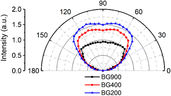
To further understand the impacts of the AlGaN barrier growth rate on the optical properties, far-field emission pattern and polarization measurements were taken. The far-field emission patterns of the DUV LEDs are presented in Fig. 4. The DUV LED with the highest growth rate, BG900, showed the lowest light intensity at each measured angle. The light intensities were augmented at all angles with the reduction of the barrier growth rate. The increases in light intensity in the far-field emission patterns are consistent with the enhancements of the light output power for the DUV LEDs with decreasing barrier growth rates. In addition, the enhancement of the light intensity at 90° was higher than those at 30° and 150°. The reduction of barrier growth rate primarily enhanced the normal emission and led to a shrink in the emission angles (the angle width at half maximum intensity) of the DUV LEDs. The normal light intensity to lateral light intensity ratio of the DUV LEDs might be related to the strain in the AlGaN/AlGaN MQWs due to the band structure change. By reducing the barrier growth rate, the surface roughness of the MQWs was diminished, and the strain in the MQWs might be altered at the same time. The large enhancement of the normal light intensity of the DUV LEDs with low barrier growth rates might be attributed to the change of the strain in the MQWs.
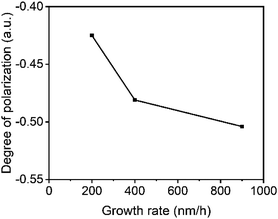
The light emission of the AlGaN-based DUV LEDs contained both TE- and TM-polarized lights, which originated from different band-to-band transitions. Many studies reported that the TE- and TM-polarized lights of AlGaN-based LEDs mainly propagate in the normal (perpendicular to the c-axis, E ⊥ c) and lateral directions (parallel to the c-axis, E ∥ c), respectively.40,41 Given that the AlGaN barrier growth rate affected the normal light intensity, polarization-dependent electroluminescence (EL) was performed to investigate the change of the TE- and TM-polarized lights of the DUV LEDs. A spectrometer was used to measure the EL spectrum of the sample at an angle of 10° to the bottom surface of the sample. The TE- and TM-polarized EL emissions could be distinguished by the polarizer (a Glan–Taylor prism) inserted between the lenses. The EL spectra of the TE- and TM-polarized lights of all the DUV LEDs are provided in Fig. S2 in the ESI.† The degree of polarization (DOP) is defined as DOP = (ITE − ITM)/(ITE + ITM), where ITE and ITM are the integrated intensities of the TE- and TM-polarized EL spectra, respectively. Fig. 5 shows that the DOP in the DUV LEDs varied with the AlGaN barrier growth rates. The DOP increased with decreasing AlGaN barrier growth rate. The result indicates that the low AlGaN barrier growth rate augmented the TE-polarized emission in the DUV LEDs. Zhang et al.45 reported that the compressive strain in the AlGaN/AlGaN MQWs could enhance the TE-polarized light emission. With the decrease of the AlGaN barrier growth rate, the increase of DOP could be attributed to the increase of the compressive strain in the MQWs. Given that the low AlGaN barrier growth rate enhanced the TE-polarized emission of the DUV LEDs, the normal light intensity of the far-field pattern was significantly increased, and the emission angle was also shrunk, as shown in Fig. 4.
To understand how the growth rate affected the AlGaN barrier, the AlN (104) X-ray diffraction reciprocal space mapping (RSM) was performed on the sample of a 400 nm-thick Al0.7Ga0.3N barrier layer grown with different growth rates to analyse the strain. The detailed epitaxial structure is presented in Fig. S3.† The structure from AlN to n-AlGaN layers was retained so that the situation of strain before growing MQWs was the same as that in the DUV LED structure. The AlN (104) RSMs of AlGaN barrier layers grown with different growth rate are presented in Fig. 6, and it was found that the contour lines of the AlGaN barrier layer shifted along the relaxation line, which meant that the strain was partially relaxed. All AlGaN barrier layers grown with different growth rates showed partial relaxation. According to the RSM data, the calculated Al composition, in-plane strain (εa), and relaxation of in-plane strain (Ra) of AlGaN barrier layers grown with different growth rates are summarized in Table 1. The εa and Ra are defined as
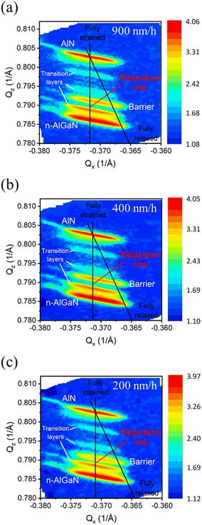 | ||
| Fig. 6 The reciprocal space mappings of AlN (104) reflection plane of barrier layers with growth rate (a) 900, (b) 400, and (c) 200 nm h−1. | ||
| Growth rate of barrier (nm h−1) | Al composition (%) | In-plane strain, εa (%) | Relaxation of in-plane strain, Ra (%) |
|---|---|---|---|
| 900 | 69.9 | −0.46 | 40.1 |
| 400 | 70.2 | −0.48 | 37.6 |
| 200 | 69.5 | −0.53 | 31.4 |
and
Finally, we compared our results to several previous reports.46–48 The flip-chip DUV LEDs with similar emission wavelengths are listed in Table 2. Zhang et al. proposed a dislocation filter (DF) layer to improve the unfavourable step-bunching morphology of AlN layer grown at a high growth rate.46 The DF layer made a transition from step-bunching to step-flow morphology, which made it feasible to grow high quality AlN at high growth rate. Hu et al. proposed a superlattice electron deceleration layer (SEDL) to improve the performance of DUV LED.47 The SEDL could decrease the electron injection current density and increase the hole injection current density. Hence, the radiative recombination rates in MQWs were raised by SEDL. Sun et al. reported the performance of DUV LED grown on nano-patterned sapphire substrates (NPSS) in combination with the optimization of V/III ratio and Si doping in MQWs.48 They also found that the IQE of MQWs was improved from 56.2% to 70.3% when the V/III ratio was increased from 500 to 1000. However, further increasing V/III from 1000 to 2000 in MQWs slightly reduced the IQE from 70.3% to 69.2%. This phenomenon could be attributed to the degradation of crystal quality of MQWs under high V/III ratio. Even if the AlGaN MQWs were grown at high V/III ratio, the crystal quality was also important. In our study, the V/III ratio was increased by lowering the growth rate of the AlGaN barrier. According to the AlN (104) RSM results, the AlGaN barrier grown at high growth rate tended to relax the strain, and the relaxation of strain usually caused defects. In other words, the barrier grown at low growth rate tended to sustain the strain, which caused fewer defects. Therefore, by lowering the growth rate, the V/III ratio was increased without degrading the crystal quality of the AlGaN barrier. Both effects were beneficial to the optical properties of MQWs. Our DUV LEDs with AlGaN barrier grown at low growth rate presented the maximum EQE of 4.27% and the maximum power enhancement of 83%, which were comparable to the previous reports. Furthermore, the DOP of DUV LEDs was increased by reducing the growth rate of the AlGaN barrier in MQWs.
| Ref. | Techniques | Structure of LED chip | Wavelength (nm) | MQWs pairs | Maximum EQE (%) | Maximum power enhancement (%) |
|---|---|---|---|---|---|---|
| 46 | Dislocation filtering (DF) layer | Flip-chip | 276.6 | 5 | 2.28 | 40.4 |
| 47 | Superlattice electron deceleration layer (SEDL) | Flip-chip | 275 | 5 | 3.43 | 200 |
| 48 | Optimization of V/III ratio and Si doping in MQWs and nano-patterned sapphire substrates (NPSS) | Flip-chip | 276.1 | 10 | 4.01 | n/a |
| This work | Reduction of barrier growth rate | Flip-chip | 279 | 5 | 4.27 | 83 |
4. Conclusions
In summary, the growth conditions of the AlGaN barrier in the AlGaN/AlGaN MQWs presented crucial influences on the light output power of the DUV LEDs. The reduction of the AlGaN barrier growth rate improved the surface roughness of the AlGaN/AlGaN MQWs, and the smooth surface could be favourable to enhancing the IQE. Furthermore, the accompanying high V/III ratio during the growth could lessen the AlGaN barrier defects. The light output power enhancement could reach 83% when the AlGaN barrier growth rate was reduced from 900 nm h−1 to 200 nm h−1. Furthermore, lowering the AlGaN barrier growth rate enhanced the normal light intensity in the far-field emission patterns and increased the DOP in the DUV LEDs. The enhanced TE-polarized emission implies that the strain in the MQWs was compressive through the decrease of the AlGaN barrier growth rate.Conflicts of interest
There are no conflicts to declare.Acknowledgements
We extend our gratitude to the National Science and Technology Council, Taiwan for their financial support under Grant Numbers: MOST 111-2221-E-006-033-MY3, MOST 107-2221-E-006-186-MY3, MOST 110-2221-E-006-153 and MOST 110-2218-E-006-025-MBK. We would also like to thank the core facility centre of the National Cheng Kung University for the support of the SEM observation and ICP etcher.References
- W. L. Morison, Phototherapy and photochemotherapy for skin disease, CRC Press, 2005 Search PubMed.
- III-Nitride Ultraviolet Emitters: Technology and Applications, ed. M. Kneissl and J. Rass, Springer, Cham, 2016 Search PubMed.
- H. Hirayama, T. Yatabe, N. Noguchi and N. Kamata, Electron. Commun. Jpn, 2010, 93, 24–33 CrossRef.
- M. Martens, F. Mehnke, C. Kuhn, C. Reich, V. Kueller, A. Knauer, C. Netzel, C. Hartmann, J. Wollweber, J. Rass, T. Wernicke, M. Bickermann, M. Weyers and M. Kneissl, IEEE Photonics Technol. Lett., 2014, 26, 342–345 CAS.
- F. Mehnke, M. Guttmann, J. Enslin, C. Kuhn, C. Reich, J. Jordan, S. Kapanke, A. Knauer, M. Lapeyrade, U. Zeimer, H. Krüger, M. Rabe, S. Einfeldt, T. Wernicke, H. Ewald, M. Weyers and M. Kneissl, IEEE J. Sel. Top. Quantum Electron., 2017, 23, 29–36 Search PubMed.
- Z. Xu and B. M. Sadler, IEEE Commun. Mag., 2008, 46, 67–73 Search PubMed.
- G. A. Shaw, A. M. Siegel, J. Model and D. Greisokh, in Unattended Ground Sensor Technologies and Applications VII, SPIE, 2005, vol. 5796, pp. 214–225 Search PubMed.
- A. Vavoulas, H. G. Sandalidis, N. D. Chatzidiamantis, Z. Xu and G. K. Karagiannidis, IEEE Commun. Surv. Tutor., 2019, 21, 2111–2133 Search PubMed.
- O. Alkhazragi, F. Hu, P. Zou, Y. Ha, Y. Mao, T. K. Ng, N. Chi and B. S. Ooi, Optical Fiber Communication Conference (OFC) 2020, OSA, 2020, p. M3I.5 Search PubMed.
- K. Kojima, Y. Yoshida, M. Shiraiwa, Y. Awaji, A. Kanno, N. Yamamoto and S. Chichibu, 2018 European Conference on Optical Communication (ECOC), 2018, pp. 1–3 Search PubMed.
- O. Alkhazragi, F. Hu, P. Zou, Y. Ha, C. H. Kang, Y. Mao, T. K. Ng, N. Chi and B. S. Ooi, Opt. Express, 2020, 28, 9111–9122 CrossRef PubMed.
- L. Guo, Y. Guo, J. Wang and T. Wei, J. Semicond., 2021, 42, 081801 CrossRef CAS.
- H. Hirayama, S. Fujikawa, N. Noguchi, J. Norimatsu, T. Takano, K. Tsubaki and N. Kamata, Phys. Status Solidi, 2009, 206, 1176–1182 CrossRef CAS.
- H. Hirayama, S. Fujikawa, J. Norimatsu, T. Takano, K. Tsubaki and N. Kamata, Phys. Status Solidi C, 2009, 6, S356–S359 Search PubMed.
- S. M. Islam, V. Protasenko, K. Lee, S. Rouvimov, J. Verma, H. Xing and D. Jena, Appl. Phys. Lett., 2017, 111, 091104 CrossRef.
- M. Shatalov, W. Sun, R. Jain, A. Lunev, X. Hu, A. Dobrinsky, Y. Bilenko, J. Yang, G. A. Garrett, L. E. Rodak, M. Wraback, M. Shur and R. Gaska, Semicond. Sci. Technol., 2014, 29, 084007 CrossRef CAS.
- C. Pernot, S. Fukahori, T. Inazu, T. Fujita, M. Kim, Y. Nagasawa, A. Hirano, M. Ippommatsu, M. Iwaya and S. Kamiyama, et al., Phys. Status Solidi, 2011, 208, 1594–1596 CrossRef CAS.
- J. R. Grandusky, S. R. Gibb, M. C. Mendrick, C. Moe, M. Wraback and L. J. Schowalter, Appl. Phys. Express, 2011, 4, 082101 CrossRef.
- N. Susilo, S. Hagedorn, D. Jaeger, H. Miyake, U. Zeimer, C. Reich, B. Neuschulz, L. Sulmoni, M. Guttmann, F. Mehnke, C. Kuhn, T. Wernicke, M. Weyers and M. Kneissl, Appl. Phys. Lett., 2018, 112, 041110 CrossRef.
- T. Takano, T. Mino, J. Sakai, N. Noguchi, K. Tsubaki and H. Hirayama, Appl. Phys. Express, 2017, 10, 031002 CrossRef.
- H. Hirayama, Y. Tsukada, T. Maeda and N. Kamata, Appl. Phys. Express, 2010, 3, 031002 CrossRef.
- R. K. Mondal, V. Chatterjee and S. Pal, Opt. Mater., 2020, 104, 109846 CrossRef CAS.
- A. Pandey, W. J. Shin, X. Liu and Z. Mi, Opt. Express, 2019, 27, A738–A745 CrossRef CAS PubMed.
- X. Wang, H.-Q. Sun and Z.-Y. Guo, Opt. Mater., 2018, 86, 133–137 CrossRef CAS.
- S. Wang, Y. A. Yin, H. Gu, N. Wang and L. Liu, J. Disp. Technol., 2016, 12, 1112–1116 CAS.
- Q. Si, H. Chen, S. Li, S. Lu and J. Kang, IEEE Photonics J., 2017, 9, 1–7 Search PubMed.
- X. Yang, H. Sun, X. Fan, Z. Zhang, J. Sun, X. Yi and Z. Guo, Superlattices Microstruct., 2017, 101, 293–298 CrossRef CAS.
- S. Sumiya, Y. Zhu, J. Zhang, K. Kosaka, M. Miyoshi, T. Shibata, M. Tanaka and T. Egawa, Jpn. J. Appl. Phys., 2008, 47, 43 CrossRef CAS.
- F. Mehnke, C. Kuhn, M. Guttmann, C. Reich, T. Kolbe, V. Kueller, A. Knauer, M. Lapeyrade, S. Einfeldt, J. Rass, T. Wernicke, M. Weyers and M. Kneissl, Appl. Phys. Lett., 2014, 105, 051113 CrossRef.
- Y. Hou and Z. Guo, Opt. Commun., 2019, 433, 236–241 CrossRef CAS.
- Y. Kuo, J. Chang, F. Chen, Y. Shih and H. Chang, IEEE J. Quantum Electron., 2016, 52, 1–5 Search PubMed.
- W. Hu, P. Qin, W. Song, C. Zhang, R. Wang, L. Zhao, C. Xia, S. Yuan, Y. Yin and S. Li, Superlattices Microstruct., 2016, 97, 353–357 CrossRef CAS.
- J. Simon, V. Protasenko, C. Lian, H. Xing and D. Jena, Science, 2010, 327, 60–64 CrossRef CAS PubMed.
- J. Zhang, W. Tian, F. Wu, W. Yan, H. Xiong, J. Dai, Y. Fang, Z. Wu and C. Chen, IEEE Photonics J., 2013, 5, 1600310 Search PubMed.
- X. Bao, P. Sun, S. Liu, C. Ye, S. Li and J. Kang, IEEE Photonics J., 2015, 7, 1–10 Search PubMed.
- H.-Y. Ryu, I.-G. Choi, H.-S. Choi and J.-I. Shim, Appl. Phys. Express, 2013, 6, 062101 CrossRef.
- K. H. Lee, H. J. Park, S. H. Kim, M. Asadirad, Y.-T. Moon, J. S. Kwak and J.-H. Ryou, Opt. Express, 2015, 23, 20340–20349 CrossRef CAS PubMed.
- Y. K. Ooi and J. Zhang, IEEE Photonics J., 2018, 10, 1–13 Search PubMed.
- P. Zhao, L. Han, M. R. McGoogan and H. Zhao, Opt. Mater. Express, 2012, 2, 1397–1406 CrossRef CAS.
- Y. K. Ooi, C. Liu and J. Zhang, IEEE Photonics J., 2017, 9, 1–12 Search PubMed.
- M. Djavid and Z. Mi, Appl. Phys. Lett., 2016, 108, 051102 CrossRef.
- Z. Bryan, I. Bryan, J. Xie, S. Mita, Z. Sitar and R. Collazo, Appl. Phys. Lett., 2015, 106, 142107 CrossRef.
- I. Bryan, Z. Bryan, S. Mita, A. Rice, L. Hussey, C. Shelton, J. Tweedie, J.-P. Maria, R. Collazo and Z. Sitar, J. Cryst. Growth, 2016, 451, 65–71 CrossRef CAS.
- K.-S. Kim, D.-P. Han, H.-S. Kim and J.-I. Shim, Appl. Phys. Lett., 2014, 104, 091110 CrossRef.
- S. Zhang, Y. Zhang, N. Tang, W. Wang, X. Chen, L. Fu, C. He, Y. Lv, Z. Feng, F. Xu, T. Yu, W. Ge and B. Shen, Superlattices Microstruct., 2021, 150, 106749 CrossRef CAS.
- Y. Zhang, H. Long, J. Zhang, B. Tan, Q. Chen, S. Zhang, M. Shan, Z. Zheng, J. Dai and C. Chen, CrystEngComm, 2019, 21, 4072–4078 RSC.
- J. Hu, J. Zhang, Y. Zhang, H. Zhang, H. Long, Q. Chen, M. Shan, S. Du, J. Dai and C. Chen, Nanoscale Res. Lett., 2019, 14, 347 CrossRef PubMed.
- Y. Sun, F. Xu, N. Zhang, J. Lang, J. Wang, B. Liu, L. Wang, N. Xie, X. Fang, X. Kang, Z. Qin, X. Yang, X. Wang, W. Ge and B. Shen, CrystEngComm, 2021, 23, 1201–1206 RSC.
Footnote |
| † Electronic supplementary information (ESI) available. See DOI: https://doi.org/10.1039/d2ra07368d |
| This journal is © The Royal Society of Chemistry 2023 |

