 Open Access Article
First-principles study on the electronic structure and photocatalytic property of a novel two-dimensional ZrS2/InSe heterojunction
Lijun Luan *,
Kaili Sun,
Di Zhang,
Kaiyang Bai,
Liuyang Han,
Changyan Xu,
Long Li and
Li Duan
School of Materials Science and Engineering, Chang'an University, Xi'an, 710064, China. E-mail: nmllj050@chd.edu.cn
First published on 11th April 2023
Abstract
Photocatalytic water cracking technology provides a broad prospect for solving the current energy crisis using solar energy and water resources. In this paper, a two-dimensional ZrS2/InSe heterojunction for accelerating the process of hydrogen production from water decomposition was constructed, and its electronic structure and photocatalytic property were studied using first-principles calculation. The results show that the lattice mismatch rate of the heterojunction from monolayer ZrS2 and monolayer InSe is 2.48%, and its binding energy is −1.696 eV, indicating that the structure of the heterojunction is stable. The ZrS2/InSe heterojunction is an indirect bandgap with a bandgap value of 1.41 eV and a typical type-II band arrangement. Importantly, the ZrS2/InSe heterostructure has a Z-scheme structure, which is beneficial to the separation of photogenerated electron hole pairs. Moreover, the ZrS2/InSe heterojunction has a strong absorption ability for visible light (up to 3.84 × 105 cm−1), which is helpful for improving its photocatalytic efficiency. The two-dimensional ZrS2/InSe heterojunction is a very promising photocatalyst, as concluded from the above studies.
Introduction
The rapid industrialization increases the demand for energy, which rapidly depletes fossil energy and seriously increases environmental pollution. Energy and environment problems have become a serious bottleneck restricting the further development of economy and society.1 Environment pollution and energy need urgent search for renewable and alternative clean energy sources to supplement and eventually replace our dependence on fossil fuels. As a new type of renewable energy, hydrogen has the advantages of low cost and zero pollution and is an ideal new energy to replace fossil fuels.2 In 1972, Fujishima and Honda3 reported a creative work, wherein they achieved hydrogen energy from light energy that was titanium dioxide single crystal used as a photoelectrode to decompose water into hydrogen under the radiation of ultraviolet light, thus realizing the conversion of light energy to hydrogen energy, which created the photocatalysis technology. Since then, the technology of using inexhaustible solar energy to split water under the action of photocatalysts to obtain clean hydrogen energy has been gaining increasing attention. Later, various kinds of bulk photocatalysts have been proposed, including metal oxides (such as TiO2,4 ZnO5), sulfides (such as CdS,6 ZnS7), nitrides (containing d0 or d10 transition metal cations8), and other new materials. Although these systematical photocatalytic activities on the bulk catalysts have been studied, it was found that most of them have some disadvantages, such as large bandgap, high recombination rate of electron–hole, poor stability, and insensitive spectral response, which seriously restrict the efficiency of photocatalytic water decomposition. Therefore, there is an urgent need to find some new light catalysts theoretically and experimentally to improve the existing photocatalytic ability.In 2004, Geim and Novoselov of the Department of Physics and Astronomy at the University of Manchester in the UK used mechanical stripping to obtain graphite with only one layer of carbon atoms, which they named as graphene.9 Since the advent of monolayer graphene, two-dimensional (2D) materials exfoliated from bulk materials have attracted more and more interest in 2D photocatalyst materials because of their larger specific surface area,10 higher carrier mobility,11 and good energy band structure.12 In recent years, many new 2D photocatalytic materials have been investigated theoretically and experimentally, such as hBN, black phosphorus (BP), transition metal dichalcogenides (TMDCs), graphite-like carbon nitride (g-C3N4), and MXenes, and have shown great potential in the field of photocatalytic splitting of water.13–17 Among them, TMDCs is a general name of a series of compounds in the form of MX2 (M is Mo, W, Zr, etc., X is S, Se, Te). Its intralayer structure is arranged as X–M–X. This special “sandwich” stacking method endows TMDCs with several unique optoelectronic properties. Zirconium disulfide (ZrS2), as one of the representatives of IV-B-TMDCs, has attracted great attention because of its good thermodynamic stability, environmental friendliness, high light sensitivity, and low production cost, and it has wide application prospects in the fields of photodetectors,18 solar cells,19 and photocatalysis.20 In recent years, monolayer ZrS2 due to these excellent properties have been successfully prepared by various experimental methods,21–23 among which the atomic layer thin ZrS2 nanowires was synthesized on conventional substrates (silica, sapphire) using optimized chemical vapor deposition (CVD) by Wang et al.,24 and photodetectors based on these thin slices were fabricated in 2015.25 Moreover, the energy band structure of ZrS2 has been proved to be a great advantage in photocatalysis.26–28 Based on the first principle, the bandgap width of monolayer ZrS2 is about 2.0 eV,29 which can maximize the use of solar light theoretically. However, because the maximum level of conduction band (CBM) is slightly smaller than the reduction potential level of hydrogen, the measured solar-hydrogen production efficiency of monolayer ZrS2 is quite lower than that of the theoretical value. To overcome these shortcomings, many methods have been explored to improve the photocatalytic performance of ZrS2. Among these, there is an effective strategy to improve the stability and photocatalytic activity of ZrS2 by building semiconductor heterostructures with other semiconductors such as graphene, g-C3N4, hBN, and ZnO.30
2D InSe materials have attracted much attention in recent years. It is a very important wide bandgap III–VI semiconductor material with high synthesis rate and stable structure. At present, monolayer InSe materials can be successfully prepared by mechanical stripping and chemical vapor transport.31 In terms of theoretical studies, the electronic and optical properties of monolayer InSe were calculated, which is an indirect bandgap semiconductor material, with a bandgap of 2.83 eV and a high ultraviolet light absorption rate. Also, the band edge position meets the requirements of photocatalytic reaction; thus, it is a promising photocatalytic material.32 However, the wide bandgap of 2.83 eV allows it to only absorb light in the wavelength range less than 438 nm, which will affect the photocatalytic performance of monolayer InSe. To solve the problem, some methods have been proposed. The light absorption range of InSe monolayer was broadened by constructing a heterojunction with Zr2CO2.33 Therefore, it is feasible to select suitable monolayer materials to form a heterojunction structure to obtain a high efficiency photocatalyst.
In this work, we chose ZrS2 and InSe materials to construct van der Waals heterostructures and systematically study their electronic structure and optical properties. In particular, the electronic structure and photocatalytic properties of 2D ZrS2, 2D InSe, and 2D ZrS2/InSe heterojunctions will be systematically explored using Perdew–Burke–Ernzerhof (PBE) functional and Heyd–Scuseria–Ernzerhof (HSE06) functional method based on density functional theory (DFT), which can provide theoretical guidance for the design and synthesis of efficient light photocatalysts in the future.
Computational methodology
Based on density functional theory (DFT), first-principles calculations were carried out using the VASP (Vienna ab initio simulation package) software package.34 We used the PBE35 functional under the generalized gradient approximation to describe the exchange correlation energy and potential. The van der Waals (vdW) correction method (DFT-D3)36 was selected to describe the interaction between ZrS2 and InSe layers. To eliminate the influence of the coupling interaction between the two adjacent layers of atoms, all calculations set up a vacuum layer of 20 Å along the z-axis. Then, in the self-consistent and property calculation, the cutoff energy of the plane wave basis set was 400 eV and the K-point grid was 4 × 4 × 1; the convergence threshold of the total energy of ion relaxation was set to 10−6 eV, and the convergence criterion of the interatomic force was 0.01 eV Å−1 to ensure the convergence accuracy of the calculation results for the most stable structure. It is well known that when using PBE functional method to calculate the bandgap of semiconductor materials, the value will lower be than the real one. Therefore, we used HSE06 functional method to accurately determine the band edge position and optical absorption spectrum of the material in the calculation of electronic and optical properties.37To evaluate the vdW interaction between 2D ZrS2 and 2D InSe, we define the binding energy (Eb) as follows.
| Eb = EZrS2/InSe − EZrS2 − EInSe | (1) |
 | (2) |
Results and discussion
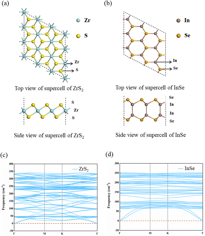
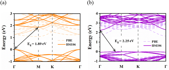
Before the ZrS2/InSe heterojunction was studied, two kinds of monolayer materials, ZrS2 and InSe, were analyzed. The structural model diagram of the ZrS2 monolayer is shown in Fig. 1(a); the solid blue circle represents Zr atom and the yellow circle represents S atom. The lattice structure of ZrS2 belongs to hexagonal closed packed (hcp) structure, and the lattice parameter of the optimized ZrS2 monolayer is a = b = 3.634 Å, which is consistent with the report in the ref. 38. Fig. 1(b) is the structural model diagram of the InSe single layer, and InSe also has an hcp structure; the solid brown circle represents In atom and the orange circle is for Se atom. The lattice constant of optimized InSe monolayer is a = b = 4.039 Å, which is consistent with the calculation result of Yang et al.39 In addition, we further calculate the phonon spectra of ZrS2 monolayer and InSe monolayer to verify their dynamic stability. Fig. 1(c) and (d) are phonon spectra of ZrS2 and InSe monolayers, respectively. It can be seen from the figure that all the phonon modes of the two monolayers do not have negative frequency, and the phonon spectrum without imaginary frequency means that the two monolayer materials have excellent dynamic stability and experimental preparation, which is the premise of constructing heterojunctions.In addition, the band structure of the ZrS2 monolayer was calculated using the PBE functional and HSE06 functional, respectively, as shown in Fig. 2(a). It can be clearly seen from diagram (a) that the energy band structure type of ZrS2 obtained by the PBE and HSE06 method is indirect bandgap. The conduction band minimum (CBM) of ZrS2 is at M point and the valence band maximum (VBM) is at Γ point both by the PBE and HSE06 methods. Fig. 2(b) shows that the band structure of InSe monolayer was calculated by the PBE functional and HSE06 functional, respectively. Fig. 2(b) also shows that both the algorithm by InSe is with an indirect bandgap; the CBM of InSe is located at Γ point, and the VBM is located between the Γ point and M point.
However, at the HSE06 level, the bandgaps of ZrS2 and InSe monolayers are 1.89 eV and 2.25 eV, respectively, and at the PBE level, the corresponding values are 1.07 eV and 1.62 eV, respectively. This result exactly supports that the bandgap value calculated by the PBE method is lower than the HSE06 method, whose result is much closer to the actual value. In addition, all the above results are in good agreement with the results of individual ZrS2 and InSe studies.32,40
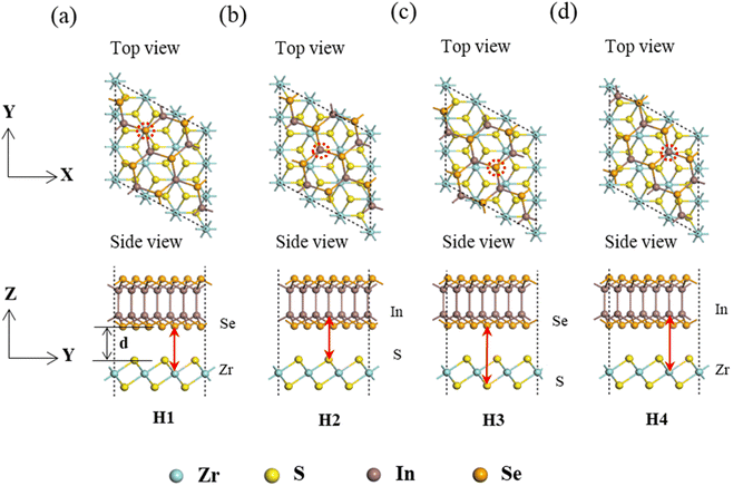
The ZrS2/InSe vdW heterojunction is constructed by combining 3 × 3 × 1 ZrS2 supercell and √7 × √7 × 1 InSe supercell. The lattice mismatch rate is calculated to be about 2.48%, which indicates that the two superprimitive cells are suitable for the construction of a heterojunction. Fig. 3 shows the top and side views of the ZrS2/InSe heterojunction model. Fig. 3(a) is the original heterojunction model, labeled ZrS2/InSe–H1. Some of the Se and Zr atoms in the ZrS2/InSe–H1 heterojunction are in the same vertical direction, marked with red double arrows in the side view and a red circle in the top view. Then, to verify that the ZrS2/InSe–H1 heterostructure is the most stable configuration, we construct three other different stacking configurations by moving the InSe layer horizontally, which were marked as ZrS2/InSe–H2, ZrS2/InSe–H3, and ZrS2/InSe–H4 heterostructures, respectively, as shown in Fig. 3(b–d). The configurations of H2, H3, and H4 correspond to In and S atoms, Se and S atoms, and In and Zr atoms in the same vertical line, respectively, and are marked with red double arrows and red circles. In Fig. 3(a), the interlayer distance is represented by d.
In addition, to verify the stability of these four different stacking structures, their lattice constants, layer spacing, and binding energy were calculated and are summarized in Table 1.
| System | Configuration | a = b/Å | LIn–In/Å | LIn–Se/Å | LZr–S/Å | d/Å | Eb/eV | /eV |
|---|---|---|---|---|---|---|---|---|
a Lattice constant (a and b), bond length (L), interlayer distance (d), binding energy (Eb), bandgap  . . |
||||||||
| ZrS2 | 3.634 | 2.581 | 1.07 | |||||
| InSe | 4.039 | 2.786 | 2.671 | 1.62 | ||||
| ZrS2/InSe | H1 | 10.826 | 2.784 | 2.672 | 2.555 | 3.132 | −1.696 | |
| ZrS2/InSe | H2 | 10.826 | 2.786 | 2.683 | 2.557 | 3.126 | −1.685 | |
| ZrS2/InSe | H3 | 10.825 | 2.789 | 2.684 | 2.557 | 3.112 | −1.684 | |
| ZrS2/InSe | H4 | 10.826 | 2.785 | 2.683 | 2.559 | 3.128 | −1.685 | |
It can be seen from Table 1 that the binding energies of these four structures are all negative, and the smaller the binding energy is, the more stable the structure. Among them, the binding energy of the ZrS2/InSe heterostructure with stacking-H1 is −1.696 eV, which is one with the lowest energy among the four configurations, which means that the stacking-H1 is the most stable structure of ZrS2/InSe heterojunction. In addition, this value of binding energy is lower than that of both the graphene/ZrS2 heterojunction (−1.67 eV) and hBN/ZrS2 heterojunction (−1.63 eV) reported by Zhang et al.30 The layer spacing of the stacking-H1 ZrS2/InSe heterojunction is 3.132 Å, which conforms to the range of the vdW interaction, indicating that it is a vdW heterojunction. Therefore, in the next study, only the stacking-H1 configuration of the ZrS2/InSe heterojunction was considered.
In addition, to evaluate the thermal stability of ZrS2/InSe–H1 heterostructures, molecular dynamics (AIMD) ab initio calculation method was used to simulate. In the AIMD simulation, the temperature is set to 300 K, the total dynamic step is set to 5000, and the time step is set to 1.0 fs. The result is shown in Fig. 4. When 5.0 ps is heated at room temperature, the energy and temperature of the heterostructure oscillate slightly with the increase in time and finally become stable and bond continuously, and there is no obvious structural change. This proves that the heterostructure of ZrS2/InSe–H1 is thermodynamically stable.
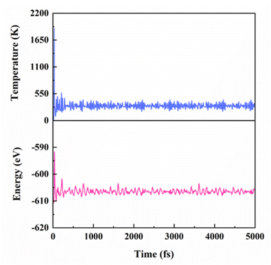 | ||
| Fig. 4 At 300 K, the temperature and energy changes of ZrS2/InSe–H1 heterostructure in AIMD simulation under continuous 5 ps. | ||
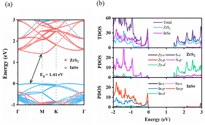
After verifying the stability of the ZrS2/InSe heterojunction, the electronic properties of the ZrS2/InSe heterojunction were explored. Fig. 5(a) shows the projected band structure of the ZrS2/InSe heterojunction calculated using the HSE06 functional. The band structure calculation results show that ZrS2/InSe heterojunction is with an indirect bandgap structure, CBM is located at the M point, VBM is between the Γ point and the M point, and the bandgap value is 1.41 eV, which conforms to the bandgap value range of photolysis water. The bandgap value of the heterojunction compared with that of monolayer ZrS2 (1.89 eV) and InSe (2.25 eV) decreases to 0.48 eV and 0.84 eV, respectively, which makes the transfer of electrons from VBM to CBM easier. The distance between the ZrS2 and InSe layers is 3.132 Å, which clearly indicates that the interaction between the ZrS2 and InSe layers is too weak to form covalent bonds. The red and blue dots in the projected energy band structure represent the contribution of monolayer ZrS2 and monolayer InSe, respectively. It is found that the VBM of the heterostructure is mainly contributed by the InSe layer, and the CBM is completely dominated by the ZrS2 layer. Therefore, the ZrS2/InSe heterojunction shows the characteristics of Type-II band arrangement. Compared with independent ZrS2 and InSe monolayers, the dispersion relation of the ZrS2/InSe heterojunction CBM is almost the same as that of two-dimensional ZrS2, while the dispersion relation of VBM is very similar to that of two-dimensional InSe.
In addition, as can be seen from the total density of states (TDOS) and the partial density of states (PDOS) of the ZrS2/InSe heterostructure in Fig. 5(b), VBM is mainly derived from InSe monolayer, and the CBM is mainly contributed by ZrS2. Further analysis of PDOS results shows that the CBM of the heterostructure mainly comes from the Zr-d orbitals of ZrS2, and the VBM mainly comes from the Se-p orbitals of InSe. This shows that the ZrS2/InSe heterojunction is a type-II van der Waals heterojunction and the electron transitions in the system will take place between different orbits for different matter. It has been proved that this type-II band structure has the characteristic of spontaneous separation of free holes and electrons, which will improve the utilization of photogenerated carriers.
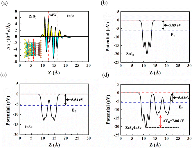
To further explore the charge transfer mechanism of the ZrS2/InSe heterostructure at the interface and reveal the mechanism for enhancing the photocatalytic activity of the system, charge density difference (CDD) and electrostatic potential near the interface of ZrS2/InSe were investigated; the result are shown in Fig. 6. For ease of presentation, the differential charge density (Δρ) is defined as follows.
| Δρ = ρZrS2/InSe − ρZrS2 − ρInSe | (3) |
The work function and plane average electrostatic potential of the material can also effectively verify the charge transfer between the interfaces. In general, the work function can be calculated by the following formula
| ϕ = Evac − EF | (4) |
Fig. 6(b)–(d) shows the electrostatic potential of single-layer ZrS2, single-layer InSe, and two-dimensional ZrS2/InSe heterojunctions along the z-axis, respectively. The results show that the work functions of ZrS2, InSe, and ZrS2/InSe heterojunctions are 5.89 eV, 5.54 eV, and 5.62 eV, respectively. Obviously, the work function of the InSe monolayer is smaller than that of the ZrS2 monolayer, which means that when the InSe monolayer interacts with the ZrS2 monolayer to form a heterojunction, the charge transfer occurs between the layers. Because the ZrS2 has a higher work function, the electrons will spontaneously transfer from the InSe layer to the ZrS2 layer until the Fermi levels of the two monolayers reach the same level. It is obvious seen from Fig. 6(d) that the electrostatic potential energy of the ZrS2 side is deeper than that of the InSe side, which is attributed to the different electronegativity of different atoms. There is a potential drop (ΔVH) of about 7.06 eV between the ZrS2/InSe heterojunction interface; thus, a built-in electric field (Eint) from InSe to ZrS2 is formed between the heterogeneous. The Eint can not only drive the photogenerated electrons to transition from the ZrS2 monolayer to the InSe monolayer but also effectively restrain the rapid recombination of photogenerated carriers in the heterojunction, thus greatly improving the photocatalytic performance.
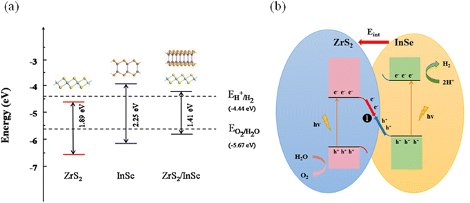
In addition, the photocatalyst should have suitable band edge positions that satisfy the oxidation and reduction potentials of water decomposition, which is an indispensable prerequisite as a photocatalyst. The potential at the bottom of the conduction band needs to be higher than the standard hydrogen potential (EH+/H2) while the potential at the top of the valence band needs to be lower than the standard oxygen potential (EO2/H2O) to meet the basic requirements of the redox reaction. When the pH = 0, the H+/H2 reduction and O2/H2O oxidation potentials are −4.44 eV and −5.67 eV, and the standard oxidation-reduction potentials increase with the increase in the pH value. Fig. 7(a) shows the band edge position of the ZrS2 layer, InSe layer, and ZrS2/InSe heterojunction. The two dotted lines represent the reduction and oxidation potential levels of water decomposition at pH = 0. The band edge of InSe monolayer is in a favorable position of photocatalysis, while the CBM of ZrS2 monolayer is slightly lower than the standard hydrogen potential, which does not meet the requirement of the band edge position of water cracking. However, the band edge position of the CBM of the constructed ZrS2/InSe heterojunction is −4.34 eV, and for the VBM, it is −5.75 eV. Then, based on the above analysis of the ZrS2/InSe heterojunction interface, Fig. 7(b) plots the photogenerated carrier transport mechanism and photocatalytic hydrolysis process of the heterojunctions. The electrons are excited from the valence band of ZrS2 (InSe) to the conduction band under the irradiation of visible light. Under the action of the built-in electric field, the photogenerated electrons transition from the ZrS2 layer to the InSe layer (path 1). At this time, the InSe with electrons will produce coulombic repulsion with a negative charge in ZrS2, resulting in the upward bending of the energy band of InSe and the downward bending of the energy band of ZrS2, thus forming a potential barrier between the conduction band (CB) of InSe and the valence band (VB) of ZrS2 under the action of an external barrier and an internal electric field. Inhibiting the transfer of electrons in the InSe conduction band to the conduction band of ZrS2 and inhibiting the transfer of holes in the ZrS2 valence band to the valence band of InSe promotes the combination of electrons in the ZrS2 conduction band and holes in the InSe valence band. Therefore, there are a large number of holes in the VB of the ZrS2 layer, and oxygen evolution occurs because of its strong oxidation: 2H2O + 4h+ → O2 + 4H+. Similarly, the CB of the InSe layer contains abundant electrons and has strong reducibility; thus, the hydrogen evolution reaction occurs as 4H+ + 4e− → 2H2. The analysis shows that the ZrS2/InSe heterojunction has a Z-type carrier transition path; thus, it is a very promising photocatalyst.
The optical absorption coefficient of the material is an important parameter to measure the photocatalytic performance of semiconductors. Therefore, the optical absorption coefficients of ZrS2, InSe, and ZrS2/InSe heterojunctions were calculated using the HSE06 functional method; the results are shown in Fig. 8. The two monolayers and ZrS2/InSe heterojunctions reached light absorption of 105 cm−1 in the ultraviolet and visible regions. The optical absorption coefficient of monolayer InSe between 243 nm and 525 nm was higher than that of the ZrS2 monolayer, and the highest light absorption coefficient could reach 3.6 × 105 cm−1 in the ultraviolet and visible regions. However, the highest optical absorption coefficient of the ZrS2 monolayer is 1.35 × 105 cm−1 in the ultraviolet and visible regions. Interestingly, compared with the two monolayer materials, the optical absorption ability of the ZrS2/InSe heterojunction is stronger than that of both the monolayer materials. In the ultraviolet region, the maximum light absorption intensity of the ZrS2/InSe heterojunction is 3.3 × 105 cm−1, and in the visible light region, the maximum light absorption intensity is 3.84 × 105 cm−1, indicating that it has good absorption capacity in the ultraviolet and visible light regions. Therefore, the ZrS2/InSe heterojunction is expected to be an efficient light photocatalyst.
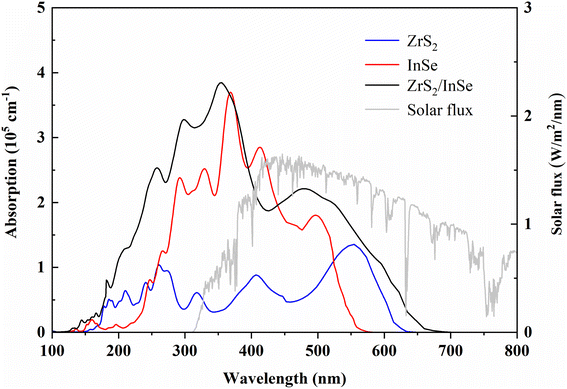 | ||
| Fig. 8 The optical absorption coefficients of monolayer ZrS2, monolayer InSe, and ZrS2/InSe heterostructures, calculated by the HSE06 method. | ||
Conclusion
In summary, on the basis of density functional theory calculations, we systematically studied the geometry and electronic properties of 2D ZrS2/InSe heterostructures and the mechanism of photocatalytic decomposition of water. First, the calculated lattice mismatch rate is 2.48%, and its binding energy is −1.696 eV, which verifies that this heterojunction is a stable heterostructure. Secondly, through the HSE06 functional calculation modified by vdW, we predict that the two-dimensional ZrS2/InSe heterostructure is an indirect bandgap structure with type-II band arrangement, its bandgap value is 1.41 eV, and it has a suitable band edge position for promoting water oxidation and reduction reaction. Furthermore, the decent band alignment of the ZrS2/InSe vdW heterostructure demonstrates a Z-scheme photocatalytic mechanism near the interface. The next optical absorption coefficient calculation shows that the ZrS2/InSe heterojunction has good absorption coefficient in the ultraviolet and visible light range (up to 3.84 × 105 cm−1). Based on the above analysis and discussion, the two-dimensional ZrS2/InSe heterostructure with good light response is expected to become a potential catalyst for the photocatalytic decomposition of water, which provides a new way for the construction of highly active photocatalysts.Conflicts of interest
We declare that we have no financial and personal relationships with other people or organizations that can inappropriately influence our work. We declare that we do not have any commercial or associative interest that represents a conflict of interest in connection with the work submitted.References
- S. Chu and A. Majumdar, Nature, 2012, 488, 294–303 CrossRef CAS PubMed
.
- X. Chen, L. Liu, P. Y. Yu and S. S. J. S. Mao, Science, 2011, 331, 746–750 CrossRef CAS PubMed
.
- K. H. A Fujishima, Nature, 1972, 238(5358), 5337–5338 CrossRef PubMed
.
- J. Yan, G. Wu, N. Guan, L. Li, Z. Li and X. Cao, Phys. Chem. Chem. Phys., 2013, 15, 10978–10988 RSC
.
- J.-H. Sun, S.-Y. Dong, J.-L. Feng, X.-J. Yin and X.-C. Zhao, J. Mol. Catal. A: Chem., 2011, 335, 145–150 CrossRef CAS
.
- J. Zhang, S. Wageh, A. Al-Ghamdi and J. Yu, Appl. Catal., B, 2016, 192, 101–107 CrossRef CAS
.
- M. Kimi, L. Yuliati and M. Shamsuddin, J. Energy Chem., 2016, 25, 512–516 CrossRef
.
- B. Luo, G. Liu and L. Wang, Nanoscale, 2016, 8, 6904–6920 RSC
.
- K. S. Novoselov, A. K. Geim, S. V. Morozov, D. Jiang, Y. Zhang, S. V. Dubonos, I. V. Grigorieva and A. A. Firsov, Science, 2004, 306, 666–669 CrossRef CAS PubMed
.
- C. Tan, X. Cao, X. J. Wu, Q. He, J. Yang, X. Zhang, J. Chen, W. Zhao, S. Han, G. H. Nam, M. Sindoro and H. Zhang, Chem. Rev., 2017, 117, 6225–6331 CrossRef CAS PubMed
.
- Y. Zhang, C. Ren, Y. Zhang, W. Lin and K. Ding, Appl. Surf. Sci., 2019, 478, 119–127 CrossRef CAS
.
- S. Ahmed and J. Yi, Nano-Micro Lett., 2017, 9, 50 CrossRef PubMed
.
- X. Sun, H. Huang, Q. Zhao, T. Ma and L. Wang, Adv. Funct. Mater., 2020, 30, 43 Search PubMed
.
- Q. Lu, Y. Yu, Q. Ma, B. Chen and H. Zhang, Adv. Mater., 2016, 28, 1917–1933 CrossRef CAS PubMed
.
- Y. Sun, Z. Sun, S. Gao, H. Cheng, Q. Liu, J. Piao, T. Yao, C. Wu, S. Hu, S. Wei and Y. Xie, Nat. Commun., 2012, 3, 1057 CrossRef PubMed
.
- Y. Sun, X. Meng, Y. Dall'Agnese, C. Dall'Agnese, S. Duan, Y. Gao, G. Chen and X. F. Wang, Nano-Micro Lett., 2019, 11, 79 CrossRef CAS PubMed
.
- Q. Liu, X. Tan, S. Wang, F. Ma, H. Znad, Z. Shen, L. Liu and S. Liu, Environ. Sci.: Nano, 2019, 6, 3170 RSC
.
- L. Li, X. Fang, T. Zhai, M. Liao, U. K. Gautam, X. Wu, Y. Koide, Y. Bando and D. Golberg, Adv. Mater., 2010, 22, 4151–4156 CrossRef CAS PubMed
.
- L. Li, H. Wang, X. Fang, T. Zhai, Y. Bando and D. Golberg, Energy Environ. Sci., 2011, 4, 5 Search PubMed
.
- R. J. Toh, Z. Sofer and M. Pumera, J. Mater. Chem. A, 2016, 4, 18322–18334 RSC
.
- M. Zhang, Y. Zhu, X. Wang, Q. Feng, S. Qiao, W. Wen, Y. Chen, M. Cui, J. Zhang, C. Cai and L. Xie, J. Am. Chem. Soc., 2015, 137, 7051–7054 CrossRef CAS PubMed
.
- S. Jeong, D. Yoo, M. Ahn, P. Miro, T. Heine and J. Cheon, Nat. Commun., 2015, 6, 5763 CrossRef CAS PubMed
.
- Z. Zeng, Z. Yin, X. Huang, H. Li, Q. He, G. Lu, F. Boey and H. Zhang, Angew. Chem., Int. Ed. Engl., 2011, 50, 11093–11097 CrossRef CAS PubMed
.
- X. Wang, L. Huang, X.-W. Jiang, Y. Li, Z. Wei and J. Li, J. Mater. Chem. C, 2016, 4, 3143–3148 RSC
.
- Z. Y. Wen Y and S. Zhang, RSC Adv., 2015, 5(81), 66082–66085 RSC
.
- A. H. Reshak and S. Auluck, Phys. B, 2004, 353, 230–237 CrossRef CAS
.
- K. B. John, P. Perdew and M. Ernzerhof, Phys. Rev. Lett., 1996, 77(18), 3865 CrossRef PubMed
.
- M. Abdulsalam and D. P. Joubert, Eur. Phys. J. B, 2015, 88, 7 CrossRef
.
- S. Li, C. Wang and H. Qiu, Int. J. Hydrogen Energy, 2015, 40, 15503–15509 CrossRef CAS
.
- X. Zhang, Z. Meng, D. Rao, Y. Wang, Q. Shi, Y. Liu, H. Wu, K. Deng, H. Liu and R. Lu, Energy Environ. Sci., 2016, 9, 841–849 RSC
.
- G. W. Mudd, S. A. Svatek, T. Ren, A. Patane, O. Makarovsky, L. Eaves, P. H. Beton, Z. D. Kovalyuk, G. V. Lashkarev, Z. R. Kudrynskyi and A. I. Dmitriev, Adv. Mater., 2013, 25, 5714–5718 CrossRef CAS PubMed
.
- B. Wang, H. Yuan, J. Chang, X. Chen and H. Chen, Appl. Surf. Sci., 2019, 485, 375–380 CrossRef CAS
.
- Y. He, M. Zhang, J.-j. Shi, Y.-l. Cen and M. Wu, J. Phys. Chem. C, 2019, 123, 12781–12790 CrossRef CAS
.
- J. D. Kresse G, Phys. Rev. B: Condens. Matter Mater. Phys., 1999, 59(53), 1758 CrossRef
.
- B. K. Perdew J P and M. Ernzerhof, Phys. Rev. Lett., 1996, 77(18), 3865 CrossRef PubMed
.
- S. Grimme, J. Antony, S. Ehrlich and H. Krieg, J. Chem. Phys., 2010, 132, 154104 CrossRef PubMed
.
- J. Heyd, G. E. Scuseria and M. Ernzerhof, J. Chem. Phys., 2003, 118, 8207–8215 CrossRef CAS
.
- Y. Si, H. Y. Wu, H. M. Yang, W. Q. Huang, K. Yang, P. Peng and G. F. Huang, Nanoscale Res. Lett., 2016, 11, 495 CrossRef PubMed
.
- L.-L. Yang, J.-J. Shi, M. Zhang, Z.-M. Wei, Y.-M. Ding, M. Wu, Y. He, Y.-L. Cen, W.-H. Guo, S.-H. Pan and Y.-H. Zhu, Chin. Phys. Lett., 2019, 36, 5 Search PubMed
.
- Y. Li, J. Kang and J. Li, RSC Adv., 2014, 4, 6 Search PubMed
.
| This journal is © The Royal Society of Chemistry 2023 |

