
 Open Access Article
 This Open Access Article is licensed under a
 Creative Commons Attribution 3.0 Unported Licence
Effect of novel graphitic carbon/NiO hole transporting electrode on the photovoltaic and optical performance of semi-transparent perovskite solar cells†
Shubhranshu Bhandari *a,
Sreeram Valsalakumara,
Yusuf Chanchangia,
Prabhakaran Selvarajab and
Tapas K. Mallicka
*a,
Sreeram Valsalakumara,
Yusuf Chanchangia,
Prabhakaran Selvarajab and
Tapas K. Mallicka
aEnvironment and Sustainability Institute, University of Exeter, Cornwall, UK TR10 9FE. E-mail: s.bhandari@exeter.ac.uk; shubhranshu0094@gmail.com
bWolfson School of Mechanical, Electrical and Manufacturing Engineering, Loughborough University, UK LE11 3TU
First published on 6th March 2023
Abstract
Perovskite devices can play a critical role as tunable semi-transparent photovoltaics managing the buildings' energy health for energy harvesting, storage and utilization. Here we report ambient semi-transparent PSCs with novel graphitic carbon/NiO-based hole transporting electrodes having variable thicknesses achieving a highest efficiency of ∼14%. On the other hand, the altered thickness produced the highest average visible transparency (AVT) of the devices, nearly 35%, which also influenced other glazing-related parameters. This study envisages the impact of the electrode deposition technique on indispensable parameters like colour rendering index, correlated colour temperature, and solar factor evaluated using theoretical models to illuminate these CPSCs' colour and thermal comfort for BIPV integration. The solar factor value between 0 to 1, CRI value >80 and CCT value >4000 K make it a significant semi-transparent device. This research work suggests a possible approach to fabricating carbon-based PSC for high-performance semi-transparent solar cells.
Introduction
Perovskite solar cells (PSCs) have explored great breakthroughs in the field of third-generation solar cells and spurred researchers to develop a variety of new architectures.1–19 These cells mainly consist of electron transport-spacer/perovskite-hole transport layers, a simple fabrication process exhibiting high power conversion efficiency (PCE) and enhanced stability towards environmental factors.20–24 Although highly efficient, PSCs sometimes rapidly lose their efficiency due to the hygroscopic and air-sensitive character of the materials used.25 Therefore, the selection of materials and their fabrication process has a significant role in the performance. PSCs often include a carbon-based back contact, a suitable solution to substitute noble metals due to their high conductivity, low cost, low-temperature processing, work function close to gold, and ambient stability.26–33 So far, various carbon polymorphs and composites have been used for PSCs as counter electrodes.34–40 The property of the counter electrode is highly crucial to determine the semi-transparent nature of PSCs as well.41–46 In this context, maintaining healthy optical and photovoltaic characters using carbon-based electrodes can be a game-changer that has not been thoroughly explored to date.Here we report the utilization of novel graphitic carbon nanoparticles (CNP) synthesized from plant materials and NiO as a hole transporting electrode (HTE) having variable thicknesses for CH3NH3PbI3 based PSCs with an FTO/compact TiO2/brookite TiO2/perovskite/graphitic CNP–NiO architecture. The method is based on a fully wet deposition process, which takes less time and utilizes a combination of spin-coating and blade-coating methods. The thickness of the HTE was varied by 1-step to 3-step deposition with a sheet resistance variation of ∼12 to ∼25 ohm. In connection, an impressive photovoltaic parameter with an overall average PCE of ∼11% was achieved for these carbon-based devices. The influence of thickness significantly altered the AVT (average visible transmittance) of the devices as well attaining an overall average of ∼31%, which influenced the calculation of the glazing-related parameters like correlated colour temperature (CCT), colour rendering index (CRI), solar factor (SF), and subjective rating (SR). We believe this finding reports an excellent combination of photovoltaics and optical performances of graphitic carbon-based PSC (CPSC) via thickness engineering as a futuristic approach for building-integrated photovoltaics.
Materials and methods
The synthesis of graphitic CNP (carbon nanoparticles) and device fabrication methods were adopted from our earlier reported article.47 The entire device fabrication process was carried out under ambient conditions for all cases. In short, fluorine doped tin oxide (FTO) glass substrate (2 cm × 2 cm) was etched, followed by standard cleaning procedures in the first place as described in ESI.† Next, 0.35 ml titanium isopropoxide (TTIP) in 0.1 ml of 2 M HCl and 5 ml ethanol was used as the precursor solution of the blocking-TiO2 layer. The compact-TiO2 layer was spin-coated at 3000 rpm for 30 s, then heated at 415 ± 10 °C for 30 minutes and cooled to room temperature. After that, the brookite TiO2 (3 wt% aqueous suspensions) layer was coated following our previous report, followed by heating at 150 °C for 30 min.48 Next, the MAPI (MAI and PbI2 were mixed in a 1![[thin space (1/6-em)]](https://www.rsc.org/images/entities/char_2009.gif) :1 molar ratio) precursor solution (4:1 DMF:DMSO) with an appropriate amount (50 μl) was spin-coated at 1000 and 5000 rpm for 10 s and 20 s, respectively. During the last 10 s of rotation, chlorobenzene (400 μl) was splashed from the top. Then the devices were heated at 100 °C for 10 min and cooled down to room temperature. Finally, the low-temperature carbon/NiO composite HTE was deposited by screen printing and heated at 100 °C for 10 min (this step was done 1 to 3 times). The carbon paste was prepared by mixing graphite (Aldrich; product number: 282863) and graphitic carbon nanoparticles (2:1 w/w) uniformly in ∼8 g terpineol via ball milling for 2 h. Then, 1.8 ml TTIP, 0.2 ml Hac (glacial acetic acid), 5 ml ethanol and 2.5 g NiO (Sigma-Aldrich; Product code: 637130) were added to the mixture by ball milling for another 10 h to gain homogenized carbon paste.
:1 molar ratio) precursor solution (4:1 DMF:DMSO) with an appropriate amount (50 μl) was spin-coated at 1000 and 5000 rpm for 10 s and 20 s, respectively. During the last 10 s of rotation, chlorobenzene (400 μl) was splashed from the top. Then the devices were heated at 100 °C for 10 min and cooled down to room temperature. Finally, the low-temperature carbon/NiO composite HTE was deposited by screen printing and heated at 100 °C for 10 min (this step was done 1 to 3 times). The carbon paste was prepared by mixing graphite (Aldrich; product number: 282863) and graphitic carbon nanoparticles (2:1 w/w) uniformly in ∼8 g terpineol via ball milling for 2 h. Then, 1.8 ml TTIP, 0.2 ml Hac (glacial acetic acid), 5 ml ethanol and 2.5 g NiO (Sigma-Aldrich; Product code: 637130) were added to the mixture by ball milling for another 10 h to gain homogenized carbon paste.
The theoretical calculations for the optical performance of devices have been detailed in the ESI.†
Results and discussions
The top surface SEM (scanning electron microscopy) of the CNP–NiO hole transporting system coated on top of a glass substrate is shown in Fig. 1a. The particle nature is very clear from the SEM, showing particle size in the range of 40 to 70 nm for the CNP and NiO. The hole transport property of NiO was the reason behind its inclusion in the CNP paste. The Device structure is shown in Fig. 1b, which indicates the small carbon bar technique to utilize the CPSC as the semi-transparent device. Depending on the number of carbon layer printing steps, the performances of the devices were analyzed. Each printing step produces ∼2 microns thick carbon layer. The sheet resistance measurement was carried out for the carbon layer depending on the number of printing steps using the Ossila four-point probe system. Table S1, ESI† shows the nature of sheet resistance according to the coating steps. Lower sheet resistance was desirable as it implies higher conductivity for the better performance of perovskite devices. These measurements helped in the understanding of the cell fabrication process. These devices consist of brookite TiO2 as an effective electron transport layer instead of high-temperature mesoporous layers, which also reduces the time and cost of fabrication. Also, brookite TiO2 and perovskite make better interfacial contact, according to previous literature.48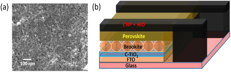 | ||
| Fig. 1 (a) Top surface SEM of carbon electrode and (b) schematic diagram of the semi-transparent PSC. | ||
The fabricated devices were initially tested with cross-sectional SEM to understand the layer thickness. The brookite and perovskite layers had thicknesses of ∼200 and ∼400 nm, respectively (Fig. S1, ESI†). Next, the photovoltaic performance was determined using the solar simulator and I–V tracer. The current density vs. voltage (J–V) characteristic measurement was performed under simulated AM 1.5 (100 mW cm−2) for the three different types of devices, as shown in Fig. 2a. Table 1 provides information about efficiency, short circuit current density (JSC), open-circuit voltage (VOC) and fill factor (FF) of the champion CPSCs of each set considering an active area of 0.12 cm2 by masking in reverse bias condition. Six devices were fabricated for each set in a batch to visualize the reproducibility of the results, as shown in Fig. S2b, ESI.† The hysteresis effect on the photovoltaic performance for champion devices has been displayed in Fig. S3, ESI,† which suggests minimal changes in forward and reverse bias conditions making the cells efficient. The average photovoltaic performances of devices are given in Table S2, ESI.† The one-step printed devices showed average PCE values of 8.5%. The two-step printed devices showed an average PCE of 10.3%. In the case of three-step coated CPSCs, an average PCE of 12.7% was observed. The effect of NiO and CNP for the devices were also observed by developing PSCs without NiO and CNP, as illustrated in Fig. S4, ESI.† The results imply maximum PCE of 10.5% and 12% for devices without NiO and CNP, respectively. Similarly, the effect of 4 step coating shows similar average PCE for the devices which implies three step coating as the saturation point.
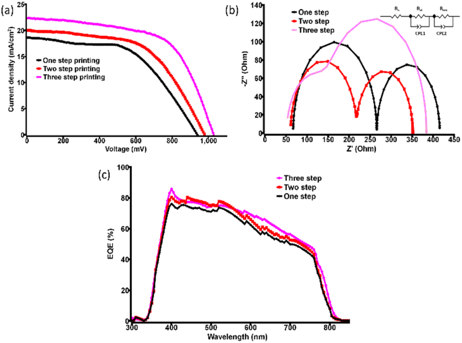 | ||
| Fig. 2 (a) Current density vs. voltage (J–V) plot for champion devices with different printing steps in reverse bias, (b) corresponding EIS spectra of the corresponding champion devices (inset: circuit diagram) and (c) IPCE measurement of the devices indicating high external quantum efficiency. | ||
| Printing step | JSC (mA cm−2) | VOC (mV) | FF (%) | PCE (%) | Integrated JSC from IPCE (mA cm−2) |
|---|---|---|---|---|---|
| One step | 18.65 | 935.4 | 55.5 | 9.68 | 17.0 |
| Two step | 20.01 | 980.6 | 58.2 | 11.4 | 18.5 |
| Three step | 22.39 | 1028.5 | 60.8 | 14.0 | 20.6 |
Further, the electrochemical impedance spectroscopy (EIS) measurements were carried out to understand the charge transport properties at different interfaces. The EIS spectrum (Nyquist plot) with the equivalent circuit diagram of the concerned CPSCs was recorded under dark at 0.9 V bias from 1 MHz to 10 mHz, as shown in Fig. 2b. The EIS analysis showed two semi-circle systems in the Nyquist plot. By using EC-lab software, the best fit was obtained for the given circuit diagram (inset Fig. 2b).
In the circuit diagram, RS represents the series resistance, including the resistance of FTO and HTE systems. RCT is the charge transfer resistance at the perovskite/carbon interface, and Rrec is the charge recombination resistance at TiO2/MAPbI3 interface.17 The small parabola in the high-frequency region for the three-step printed device indicates lower charge exchange resistance from perovskite to carbon counter electrode (HTE), enhancing the fill factor as reflected from J–V characterization. On the other hand, the large Rrec value implies a slow charge recombination process or a low charge recombination rate. This low recombination rate is responsible for high values of JSC and VOC, which are reflected in the J–V curves. Devices with higher RS values should have lower efficiency, which can be observed in Table 2.
| Printing step | RS (ohm) | RCT (ohm) | Rrec (ohm) |
|---|---|---|---|
| One step | 67.1 | 198.8 | 149.8 |
| Two step | 60.74 | 133.9 | 156.7 |
| Three step | 51.8 | 94.14 | 238.0 |
The other important factor in confirming the nature of devices was incident photon to electron conversion efficiency (IPCE) determination. It showed high external quantum efficiency (EQE) for the devices, as displayed in Fig. 2c and the integrated current density values closely matched with J–V data. Fig. 2c also implies nice IPCE coverage in the range of 400 to 700 nm for different champion devices indicating good perovskite film quality. To clarify the reliability of the cell performance box and whiskers plot of the PCE for each type of device is given in Fig. S2, ESI.† After realizing the device's photovoltaic properties, the semi-transparent nature of the CPSCs was examined. The transmittance of the different sets of devices is shown in Fig. 3 (data obtained from UV-visible spectrophotometer), which implies the highest AVT for the single-step printed devices. The AVT values observed for the champion device of each set are given in Table 3. An impressive value of 34.3% was noticed for the single-step coating of the counter electrode in CPSC, although the photovoltaic performances of these devices are the poorest. AVT of devices without any carbon bar HTE system was also observed to understand the difference, which showed an impressive value of >50%. The inclusion of three layers severely damages the AVT of the devices, although they have produced better photovoltaic data. Next, different glazing-related parameters were calculated for these CSPCs using theoretical models and equations following previous literature.42 CCT and CRI are two important parameters for glazing purposes. Typically a CCT value between 3000 and 7000 K is suitable for entering daylight through glazing. On the other hand, a CRI value near 100 is highly favourable, although values ≥80 are also acceptable. The observed CCT and CRI values for prepared CPSCs are fascinating, as shown in Fig. 4. The highest CCT and CRI were observed for the devices with lower AVT, i.e. the triple-printed devices showed higher CCT and CRI along with high PCE values as well (Table 3).
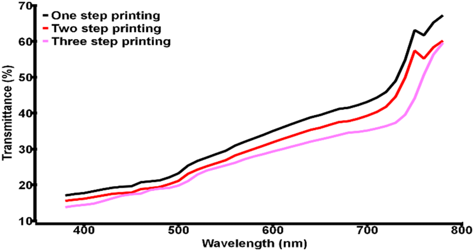 | ||
| Fig. 3 Transmittance vs. wavelength plot for the champion devices with various printing steps. | ||
| Printing step | AVT (%) | CCT (K) | CRI | SF |
|---|---|---|---|---|
| One step | 34.3 | 4436.09 | 80.3 | 0.57 |
| Two step | 31.2 | 4318.52 | 80.4 | 0.53 |
| Three step | 28.4 | 4547.68 | 82.1 | 0.52 |
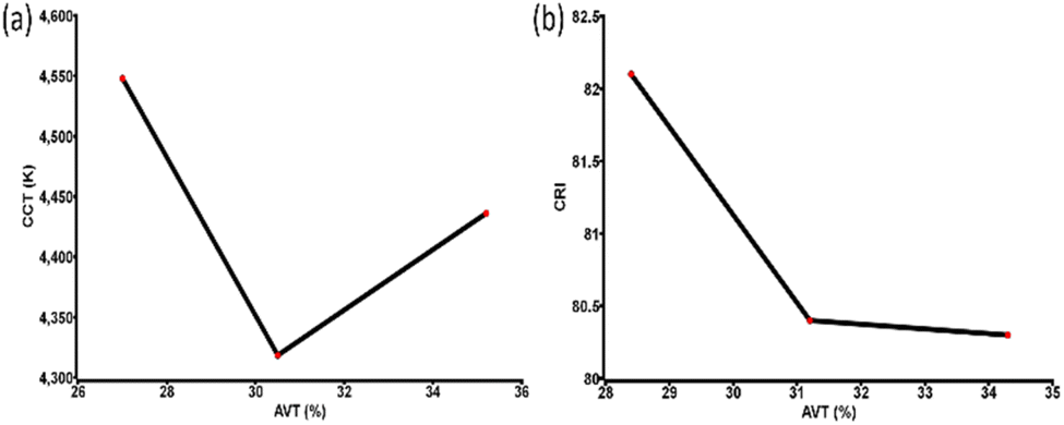 | ||
| Fig. 4 (a) CCT vs. AVT and (b) CRI vs. AVT of the champion devices fabricated by variable electrode deposition steps. | ||
Further, the SF and SR of the devices were evaluated. The SF value indicates the protection parameter from the solar radiation, which is usually between 0 to 1. The value near zero implies the best protection from solar radiation. The SF values significantly suggest the lowest value for the lower AVT based devices pointing to more suitable protection from solar radiation. Table 3 and Fig. 5a give the idea of the SF parameter. The trends reflect convenient colour comfort as well as radiation control for the devices having lower values of AVT and higher PCE.
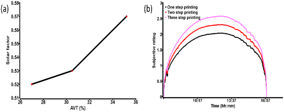 | ||
| Fig. 5 (a) SF vs. AVT of the champion CPSCs considering each type and (b) SR of the champion devices considering a clear sunny day of Cornwall in Summer. | ||
Finally, the SR of the CPSCs were considered taking into account the clear sunny day of Cornwall during the summer, as shown in Fig. 5b. SR dictates the glare daylight control potential, and values ≥2.5 become intolerable. The fabricated devices showed the potential for daylight control during the clear sunny day of summer, which makes them highly suitable for cloudy or intermittent cloudy conditions.
Noticeably the SR value is near the acceptable range for the devices with higher AVT. Although high PCE devices have better protection from solar radiation, they lack daylight control through glazing. This indicates the difficulty of attaining colour comfort and glare daylight control potential in the same device.
Finally, the stability of the devices was observed under ambient conditions kept in the dark. Devices with one-step coating were found to be less stable compared to three-step CNP coating. Usually, carbon as a counter electrode protects devices from atmospheric (air and moisture mainly) interaction; thus, the thickness of the HTE produced the differences in stability, as shown in Fig. S5, ESI.† The maximum stability of three-step carbon-coated devices was ∼600 h with a loss of approximately 10% of initial efficiency.
Conclusion
In this work, semi-transparent CPSCs were fabricated under ambient conditions, and performances (photovoltaic and optical) were investigated depending on the electrode printing technique. Low-temperature graphitic CNP–NiO HTE system significantly influenced the performances. The AVT value of 34.3% for CPSC makes this study significant, although the device with the highest PCE (14%) attained the lowest value of AVT (28.4%). Optical parameters like CCT, CRI, SF and SR have shown remarkable values that dictate the carbon-based device's potential. This study is noteworthy for more detailed future research to unveil the possibilities of CPSC for building integrated photovoltaic systems by incorporating low-temperature procedures to save time and cost.Author contributions
Shubhranshu Bhandari: Conceptualization, Methodology, Formal analysis, Investigation, Writing – original draft, Visualization. Sreeram Valsalakumar: Investigation, Writing – review & editing, Visualization. Yusuf Chanchangi: Investigation, Writing – review & editing, Visualization. Prabhakaran Selvaraj: Investigation, Writing – review & editing, Visualization. Tapas Mallick: Writing – review & editing, Visualization, Supervision, Project administration, Funding acquisition.Conflicts of interest
There are no conflicts to declare.Acknowledgements
The funding from Engineering and Physical Science Research Council (EPSRC) is acknowledged.References
- G. Huang, C. Wang, H. Zhang, S. Xu, Q. Xu and Y. Cui, J. Mater. Chem. A, 2018, 6, 2449–2455 RSC.
- Y. Rong, X. Hou, Y. Hu, A. Mei, L. Liu, P. Wang and H. Han, Nat. Commun., 2017, 8, 14555 CrossRef PubMed.
- D. H. Kim, G. S. Han, W. M. Seong, J.-W. Lee, B. J. Kim, N.-G. Park, K. S. Hong, S. Lee and H. S. Jung, ChemSusChem, 2015, 8, 2392–2398 CrossRef CAS PubMed.
- J.-Y. Seo, R. Uchida, H.-S. Kim, Y. Saygili, J. Luo, C. Moore, J. Kerrod, A. Wagstaff, M. Eklund, R. McIntyre, N. Pellet, S. M. Zakeeruddin, A. Hagfeldt and M. Grätzel, Adv. Funct. Mater., 2018, 28, 1705763 CrossRef.
- L. Zhu, Z. Shao, J. Ye, X. Zhang, X. Pan and S. Dai, Chem. Commun., 2016, 52, 970–973 RSC.
- B. Kim, S. G. Ko, K. S. Sonu, J. H. Ri, U. C. Kim and G. Il Ryu, J. Electron. Mater., 2018, 47, 6266–6271 CrossRef CAS.
- W. Chen, X. Yin, M. Que, H. Xie, J. Liu, C. Yang, Y. Guo, Y. Wu and W. Que, J. Power Sources, 2019, 412, 118–124 CrossRef CAS.
- H.-S. Kim, C.-R. Lee, J.-H. Im, K.-B. Lee, T. Moehl, A. Marchioro, S.-J. Moon, R. Humphry-Baker, J.-H. Yum, J. E. Moser, M. Grätzel and N.-G. Park, Sci. Rep., 2012, 2, 591 CrossRef PubMed.
- Z. Wang, J. Fang, Y. Mi, X. Zhu, H. Ren, X. Liu and Y. Yan, Appl. Surf. Sci., 2018, 436, 596–602 CrossRef CAS.
- K. Cao, Z. Zuo, J. Cui, Y. Shen, T. Moehl, S. M. Zakeeruddin, M. Grätzel and M. Wang, Nano Energy, 2015, 17, 171–179 CrossRef CAS.
- S. Liu, W. Huang, P. Liao, N. Pootrakulchote, H. Li, J. Lu, J. Li, F. Huang, X. Shai, X. Zhao, Y. Shen, Y.-B. Cheng and M. Wang, J. Mater. Chem. A, 2017, 5, 22952–22958 RSC.
- Y. Yang, K. Ri, A. Mei, L. Liu, M. Hu, T. Liu, X. Li and H. Han, J. Mater. Chem. A, 2015, 3, 9103–9107 RSC.
- S. S. Mali, H. Kim, J. V Patil and C. K. Hong, ACS Appl. Mater. Interfaces, 2018, 10, 31280–31290 CrossRef CAS PubMed.
- N.-G. Park, J. Phys. Chem. Lett., 2013, 4, 2423–2429 CrossRef CAS.
- Z. Ku, Y. Rong, M. Xu, T. Liu and H. Han, Sci. Rep., 2013, 3, 3132 CrossRef PubMed.
- T. Liu, Y. Xiong, A. Mei, Y. Hu, Y. Rong, M. Xu, Z. Wang, L. Lou, D. Du, S. Zheng, X. Long, S. Xiao, S. Yang and H. Han, RSC Adv., 2019, 9, 29840–29846 RSC.
- S. Liu, K. Cao, H. Li, J. Song, J. Han, Y. Shen and M. Wang, Sol. Energy, 2017, 144, 158–165 CrossRef CAS.
- M. M. Lee, J. Teuscher, T. Miyasaka, T. N. Murakami and H. J. Snaith, Science, 2012, 338, 643–647 CrossRef CAS PubMed.
- F. Giordano, A. Abate, J. P. Correa Baena, M. Saliba, T. Matsui, S. H. Im, S. M. Zakeeruddin, M. K. Nazeeruddin, A. Hagfeldt and M. Graetzel, Nat. Commun., 2016, 7, 10379 CrossRef CAS PubMed.
- A. Abate, J.-P. Correa-Baena, M. Saliba, M. S. Su’ait and F. Bella, Chem.–Eur. J., 2018, 24, 3083–3100 CrossRef CAS PubMed.
- N. Torabi, A. Behjat, Y. Zhou, P. Docampo, R. J. Stoddard, H. W. Hillhouse and T. Ameri, Mater. Today Energy, 2019, 12, 70–94 CrossRef.
- S. Bhandari, A. Roy, T. K. Mallick and S. Sundaram, Mater. Lett., 2020, 268, 127568 CrossRef CAS.
- M. Khalid, A. Roy, S. Bhandari, P. Selvaraj, S. Sundaram and T. K. Mallick, J. Alloys Compd., 2022, 895, 162626 CrossRef CAS.
- M. S. Sheikh, A. Roy, S. Bhandari, T. K. Mallick, S. Sundaram and T. P. Sinha, Mater. Lett., 2020, 276, 128220 CrossRef CAS.
- R. Wang, M. Mujahid, Y. Duan, Z.-K. Wang, J. Xue and Y. Yang, Adv. Funct. Mater., 2019, 29, 1808843 CrossRef CAS.
- S. Collavini and J. L. Delgado, Adv. Energy Mater., 2017, 7, 1601000 CrossRef.
- S. N. Habisreutinger, T. Leijtens, G. E. Eperon, S. D. Stranks, R. J. Nicholas and H. J. Snaith, Nano Lett., 2014, 14, 5561–5568 CrossRef CAS PubMed.
- Q.-Q. Chu, B. Ding, J. Peng, H. Shen, X. Li, Y. Liu, C.-X. Li, C.-J. Li, G.-J. Yang, T. P. White and K. R. Catchpole, J. Mater. Sci. Technol., 2019, 35, 987–993 CrossRef CAS.
- X. Wu, L. Xie, K. Lin, J. Lu, K. Wang, W. Feng, B. Fan, P. Yin and Z. Wei, J. Mater. Chem. A, 2019, 7, 12236–12243 RSC.
- R. Hu, R. Zhang, Y. Ma, W. Liu, L. Chu, W. Mao, J. Zhang, J. Yang, Y. Pu and X. Li, Appl. Surf. Sci., 2018, 462, 840–846 CrossRef CAS.
- S. Wang, P. Jiang, W. Shen, A. Mei, S. Xiong, X. Jiang, Y. Rong, Y. Tang, Y. Hu and H. Han, Chem. Commun., 2019, 55, 2765–2768 RSC.
- F. Meng, L. Gao, Y. Yan, J. Cao, N. Wang, T. Wang and T. Ma, Carbon, 2019, 145, 290–296 CrossRef CAS.
- X. Xu, Z. Liu, Z. Zuo, M. Zhang, Z. Zhao, Y. Shen, H. Zhou, Q. Chen, Y. Yang and M. Wang, Nano Lett., 2015, 15, 2402–2408 CrossRef CAS PubMed.
- F. Meng, A. Liu, L. Gao, J. Cao, Y. Yan, N. Wang, M. Fan, G. Wei and T. Ma, J. Mater. Chem. A, 2019, 7, 8690–8699 RSC.
- Y. Rong, L. Liu, A. Mei, X. Li and H. Han, Adv. Energy Mater., 2015, 5, 1501066 CrossRef.
- M. Batmunkh, C. J. Shearer, M. J. Biggs and J. G. Shapter, J. Mater. Chem. A, 2015, 3, 9020–9031 RSC.
- X. Cai, J. Tang, M. Zhao, L. Liu, Z. Yu, J. Du, L. Bai, F. Lu, T. Jiu and Y. Li, Nano Res., 2022, 15, 9734–9740 CrossRef CAS.
- W. Yu, X. Sun, M. Xiao, T. Hou, X. Liu, B. Zheng, H. Yu, M. Zhang, Y. Huang and X. Hao, Nano Res., 2022, 15, 85–103 CrossRef CAS.
- M. Sun, J. Shu, C. Zhao, J. Wu, H. Guo, Y. Guo, X. Yin, Y. Lin, Z. Tan, M. He and L. Wang, ACS Appl. Mater. Interfaces, 2022, 14, 13352–13360 CrossRef CAS PubMed.
- X. Yin, Y. Guo, Z. Xue, P. Xu, M. He and B. Liu, Nano Res., 2015, 8, 1997–2003 CrossRef CAS.
- A. Roy, A. Ghosh, S. Bhandari, S. Sundaram and T. K. Mallick, Build, 2020, 10 Search PubMed.
- S. Bhandari, A. Ghosh, A. Roy, T. K. Mallick and S. Sundaram, Chem. Eng. J. Adv., 2022, 10, 100267 CrossRef CAS.
- B. Shi, L. Duan, Y. Zhao, J. Luo and X. Zhang, Adv. Mater., 2020, 32, 1806474 CrossRef CAS PubMed.
- H.-C. Kwon and J. Moon, Curr. Opin. Electrochem., 2018, 11, 114–121 CrossRef CAS.
- M. Saifullah, J. Gwak and J. H. Yun, J. Mater. Chem. A, 2016, 4, 8512–8540 RSC.
- F. R. Li, Y. Xu, W. Chen, S. H. Xie and J. Y. Li, J. Mater. Chem. A, 2017, 5, 10374–10379 RSC.
- S. Bhandari, A. Roy, M. S. Ali, T. K. Mallick and S. Sundaram, Sci. Rep., 2021, 11, 23388 CrossRef CAS PubMed.
- S. Bhandari, A. Roy, T. K. Mallick and S. Sundaram, Chem. Eng. J., 2022, 446, 137378 CrossRef CAS.
Footnote |
| † Electronic supplementary information (ESI) available. See DOI: https://doi.org/10.1039/d2ra08198a |
| This journal is © The Royal Society of Chemistry 2023 |