
 Open Access Article
 This Open Access Article is licensed under a
 Creative Commons Attribution 3.0 Unported Licence
Near-infrared to visible and ultraviolet upconversion in TiO2 thin films modified with Er and Yb
Anna Śliz *a,
Marta Radeckaa,
Piotr Jeleńa,
Dominik Dorosza and
Katarzyna Zakrzewskab
*a,
Marta Radeckaa,
Piotr Jeleńa,
Dominik Dorosza and
Katarzyna Zakrzewskab
aFaculty of Materials Science and Ceramics, AGH University of Science and Technology, al. A. Mickiewicza 30, 30-059 Kraków, Poland. E-mail: annakot@agh.edu.pl
bFaculty of Computer Science, Electronics and Telecommunications, AGH University of Science and Technology, al. A. Mickiewicza 30, 30-059 Kraków, Poland
First published on 7th March 2023
Abstract
Upconversion as a modification strategy to enhance the utilization of sunlight in titanium dioxide photoanodes with an internal upconverter was investigated. TiO2 thin films containing an Er activator and Yb sensitizer were deposited in the magnetron sputtering process on conducting glass, amorphous silica, and silicon. Scanning electron microscopy, energy dispersive spectroscopy, grazing incidence X-ray diffraction, and X-ray absorption spectroscopy allowed assessment of the thin film composition, structure, and microstructure. Optical and photoluminescence properties were measured by means of spectrophotometry and spectrofluorometry. Changing the content of Er3+ (1, 2, 10 at%) and Yb3+ (1, 10 at%) ions allowed us to achieve thin film upconverters with a crystallized and amorphous host. Upon 980 nm laser excitation Er3+ exhibits upconversion with the main emission in green (2H11/2 → 4I15/2, λem ≈ 525 nm) and weak emission in red (4F9/2 → 4I15/2, λem ≈ 660 nm). For a thin film with a higher ytterbium content (10 at%) a significant increase in red emission and upconversion from NIR to UV was observed. The average decay times of green emission for TiO2:Er and TiO2:Er,Yb thin films were calculated based on time-resolved emission measurements.
Introduction
Lanthanide ions (Ln3+), along with transition metal ions and organic molecules, are well known to be luminescent centers in materials.1,2 The ladder-like structure of Ln3+ with abundant 4f energy levels enables multiple intraconfigurational transitions and allows not only light emission according to Stokes law but also the upconversion (UC) of two or more low-energy photons into a photon of a higher energy in the anti-Stokes upconversion process.3 Upconversion nanomaterials find applications in photonics, biomedicine, sensors, photocatalysis, photovoltaics, and photoelectrochemical cells.4–10A typical upconversion material consists of emitting ions (activator), and optionally enhancing ions (sensitizer), embedded in a matrix (host).8,11,12 Er3+ ions are one of the extensively studied activator ions for upconversion from near-infrared (NIR) to visible (VIS), red and green, and ultraviolet (UV) regions (390–410 nm), which is due to an appropriate energy level structure.11 To enhance the absorption of infrared photons an Yb3+ sensitizer is added, due to its large absorption cross-section in NIR compared to other Ln3+ ions (9.11 × 10⁻²¹ cm−2 at 980 nm excitation).13 When ytterbium ions absorb infrared photons, electrons are excited from the 2F7/2 ground state to the higher energetic state. The excited state 2F5/2 of Yb3+ matches the f–f transitions in Ln3+ activators, for example it overlaps the 4I11/2 state of Er3+, thus excessive energy can be transferred to activator ions by the energy transfer mechanism.14 Choice of the host material is crucial due to its impact on the upconversion ability, emission intensity, and wavelength of emitted light.5,11,12,15 To achieve efficient luminescence, the host should be a low phonon material, which decreases the rate of non-radiative relaxation, with a good distribution of a high amount of activator ions to avoid cross-relaxation mechanisms. Usually, for inorganic upconversion materials fluorides (NaYF4), oxides (ZrO2, Y2O3, SiO2, TiO2), oxyhalides (GdOCl), oxysulfides (La2O2S), and phosphates (LuPO4, YPO4) are used as hosts.5
TiO2, in polymorphic forms of anatase, rutile and brookite, is an important semiconductor for photocatalysis and photoelectrochemical cells (PEC).16–18 In particular, its ability to utilize solar energy to split water into hydrogen and oxygen is applicable for green solar energy. However, the wide bandgap of TiO2 (Eg, rutile = 3.0 eV, Eg, anatase = 3.2 eV) limits light harvesting to UV, while VIS and NIR light are underutilized (sub-bandgap energy photons) and thus modification strategies such as microstructure modification, doping, formation of heterostructures, bandgap engineering, and enhancement by the upconversion process are investigated.16,17 The last mentioned strategy does not rely on the modification of TiO2 properties to better fit the solar spectrum, but rather on the change of the light distribution. Combining TiO2 with UC materials allows to absorb additional photons from the NIR range, then upconvert them to visible and UV that can excite TiO2.
To the best of our knowledge, the application of upconverters in photoelectrochemical cells for water splitting, contrary to well-developed upconverters for photovoltaic cells or photocatalysts, is still an unexploited research area.17,19,20 Moreover, most of the investigated UC materials are in the form of powders21 or bulk materials,22 like optical fibers, while upconversion thin film materials remain a challenge. To achieve upconversion and maintain good photoelectrochemical performance in case of a few hundred nanometers thick TiO2 film photoanode, it is important to find a balance between introducing a high amount of activator and sensitizer ions, their distribution in the host, and obtaining proper structure and microstructure of TiO2. In general, a higher activator concentration increases the possibility of upconversion, but after reaching a certain level, the activator ions are too close to each other and the UC efficiency is lowered due to the cross-relaxation mechanism. Meanwhile, the sensitizer ions need short distances between the ions, which allows for non-radiative energy transfer. Thus, another strategy is to keep the activator ion concentration at a low level, but with the addition of a sensitizer. In that way, the amount of activator ion can be reduced to a few mol%, while for the sensitizer it can reach a high concentration (≈20 mol%).17 Salhi and Deschanvres23 prepared crystallized TiO2 powders with 5 mol% Er and 10 mol% Yb via hydrothermal method. However, a high concentration of Ln3+ ions, due to significantly larger ionic radii than Ti4+, leads to the amorphization of TiO2. Pérez et al.24 investigated TiO2 films with Er3+ ions doping concentration up to 10 at%, for which diffraction peak of (1 0 1) anatase plane was still observable, but the amorphous TiO2 phase was dominant. Johannsen et al.25 showed that changes in host crystallinity in Er3+ doped TiO2 films deposited on Si (100) substrates significantly modified its luminescence properties. Moreover, red-to-green emission ratio relate to Er3+/Yb3+ concentration ratio as presented by Jung,26 while blue or UV light emission is observed only for UC materials with high efficiency due to low probability of the three or four photon UC processes.9
In our previous works, we investigated both the concepts of external27 and internal upconverter,28,29 and we demonstrated the possibility to use TiO2 thin film photoanodes modified with rare earth ions (Nd3+, Er3+, Yb3+) in photoelectrochemical cells.27,29 Thin film photoanodes deposited at 20% O2/(O2 + Ar) flow rate ratio exhibit the best photoelectrochemical properties (high value of photocurrent and rectangular shape of current density versus voltage curves).27 In our research on photoanodes with internal upconverter, we examined two strategies: introduction of high activator content (TiO2:Er (10 at%)) or incorporation of the low activator content with the addition of sensitizer (TiO2:Er,Yb (1 at%, 1 at%) and TiO2:Er,Yb (2 at%, 10 at%)). Recently, we described the photoelectrochemical properties of such photoanode materials.29 Here, we would like to focus on the investigation of TiO2 modified with Er and Yb thin films luminescence properties and the influence of the surrounding host on the lanthanide ions upconversion ability. We compare thin film upconverters with crystallized and amorphous host, which was achieved by changing the content of Er3+ and Yb3+ ions.
Experimental
TiO2, TiO2:Er and TiO2:Er,Yb thin films were deposited in reactive radio frequency magnetron sputtering in an ultra-high vacuum system (PREVAC). The base vacuum in the process chamber, after heating up the substrates to 350 °C, was at the level of 10−7–10−8 mbar. During deposition, the argon and oxygen flow rates were set at 32 sccm and 8 sccm, respectively to keep 20% O2/(O2 + Ar) flow rate ratio, and the working pressure at the level of 6–7 × 10⁻³ mbar. Sputtering of 2′′ targets (Kurt Lesker Ltd) with diverse compositions, Ti, Ti/Er (90/10 at%), Ti/Er/Yb (98/1/1 at%), and Ti/Er/Yb (88/2/10 at%), was performed with a power density of 9–10 W cm−2. More details of process steps and parameters are described in our previous work.28 Thin films were deposited on various substrates: amorphous silica (Q) for investigation of the thin film structure, and to assess the impact of rare earth ions on the optical bandgap of the TiO2 host, silicon (Si) for observation of the thin film microstructure and further investigation of its structural properties, conducting indium tin oxide glass (ITO) to assess luminescence properties of upconversion photoanodes.The average thickness of the deposited films was measured with a Rank Taylor Hobson Talystep stylus surface profilometer. The structure of the deposited thin films was determined by means of grazing incidence X-ray diffractometry (GIXRD) with a Philips X'Pert MPD diffractometer (λCu = 0.154 nm). The diffractograms, with a subtracted background that originates from the silica substrate, were analysed according to data from the International Centre for Diffraction Data (ICDD) database (anatase 01-078-2486 and rutile 01-086-0147 cards). Scanning electron microscopy (SEM) imaging with energy dispersive spectroscopy (EDS) analysis was performed using Thermo Fischer Scientific Helios G4-PFIB-CXe microscope. For further structural investigation, X-ray absorption spectroscopy (XAS) measurements were conducted at SOLARIS National Synchrotron Radiation Centre in Kraków, Poland. XAS spectra were collected with synchrotron soft X-ray radiation at the PIRX beamline (Premiere InstRument for XAS, former PEEM/XAS). A more detailed description of the experimental procedure at the PIRX beamline is described in ref. 30. Measurements were carried out with 1 s per point acquisition time and energy steps of 0.05 eV for the pre-edge and white line range, and 0.1 eV over the range free from any sharp absorption peaks. Transmittance (T) and reflectance (R) spectra were measured with the UV-VIS-NIR Perkin Elmer double beam Lambda 19 spectrophotometer. Triax 180 Jobin Yvon grating monochromator with 450 W xenon lamp equipped with optical fiber and lens was used as a light source for photoelectrochemical experiments. Current versus time characteristics (I–t) were recorded under monochromatic illumination, changing the wavelength from 300 to 420 nm with a 10 nm step. 0.8 M Na2SO4 solution and a three electrode setup (working electrode – sample, auxiliary electrode – platinum foil covered with platinum black, reference electrode – Ag/AgCl in 3 M KCl) was used. The MTM Anko M161E electrochemical analyser served as a potentiostat for I–t measurements. Raman and photoluminescence spectra were collected with the WITec Alpha 300M+ spectrometer equipped with a 488 nm laser, the Zeiss LD EC 50× objective, and a CCD UV-NIR detector. Measurements in the 0–15![[thin space (1/6-em)]](https://www.rsc.org/images/entities/char_2009.gif) 000 cm−1 wavenumber range were conducted in multiple scans, while each scan consisted of 2 seconds acquisition and 2 accumulations. Upconversion steady-state luminescence spectra and time-resolved emission measurements were performed in Horiba Fluorolog-QM-75-12C spectrofluorometer equipped with 700 mm double monochromator and photon counting PMT 920 IS detector with thermoelectric cooling, upon 980 nm semiconductor laser diode (LD) excitation.
000 cm−1 wavenumber range were conducted in multiple scans, while each scan consisted of 2 seconds acquisition and 2 accumulations. Upconversion steady-state luminescence spectra and time-resolved emission measurements were performed in Horiba Fluorolog-QM-75-12C spectrofluorometer equipped with 700 mm double monochromator and photon counting PMT 920 IS detector with thermoelectric cooling, upon 980 nm semiconductor laser diode (LD) excitation.
Results and discussion
Thin film samples are named according to the composition of the sputtering targets. The list of samples with target composition, temperature of substrate during deposition, deposition rate, and thickness measured with the profilometer can be found in Table 1.| Sample name | Target | Substrate heating temperature (°C) | Deposition rate (nm min−1) | Thickness (nm) |
|---|---|---|---|---|
| TiO2 crystallized | Ti | 350 | 11.0 | 320 |
| TiO2:Er (10 at%) | Ti/Er (90/10 at%) | 350 | 7.7 | 230 |
| TiO2:Er,Yb (1 at%, 1 at%) | Ti/Er/Yb (98/1/1 at%) | 350 | 11.3 | 340 |
| TiO2:Er,Yb (2 at%, 10 at%) | Ti/Er/Yb (88/2/10 at%) | 350 | 8.2 | 270 |
| TiO2 amorphous | Ti | No heating | 7.3 | 220 |
To investigate the structure, microstructure and determine the elemental composition of thin films, GIXRD, SEM and EDS measurements were conducted (Fig. 1). Analysis of top-view SEM images and diffractograms showed that a high addition of Er and Yb ions caused amorphization of thin films, a decrease in average grain size, and a smooth surface compared to crystallized pure TiO2 or thin film with a low addition of Er and Yb. Crystallized TiO2 and TiO2:Er,Yb (1 at%, 1 at%) films have grains with pyramid-like tops with average grain size 57 and 52 nm, respectively. Anatase is a dominant phase, whereas rutile and a trace of brookite phase are also observed. For amorphous TiO2:Er (10 at%) the average grain size was 26 nm and for TiO2:Er,Yb (2 at%, 10 at%) 18 nm. It was reported that a high concentration of Er3+ seems to stabilize the TiO2 amorphous phase or hinder the crystallization.31 The ionic radii of Er3+ and Yb3+, 89 pm and 86 pm respectively, are significantly larger than Ti4+ ionic radius (68 pm). This mismatch has an impact on lattice distortion of TiO2.20,32,33 Therefore, substitution of Ti4+ in its lattice site is less probable than interstitial incorporation or segregation of Ln3+ ions at the grain boundaries.20 The EDS elemental analysis results (Fig. 1), considering the semi-quantitative character of this technique, correlate well with the composition of the targets used for the sputtering. In all EDS spectra, due to the beam penetration depth larger than film thickness, besides peaks from elements in the thin film (Ti, O, Er, and Yb), a high-intensity peak originating from the substrate (Si) is observed.
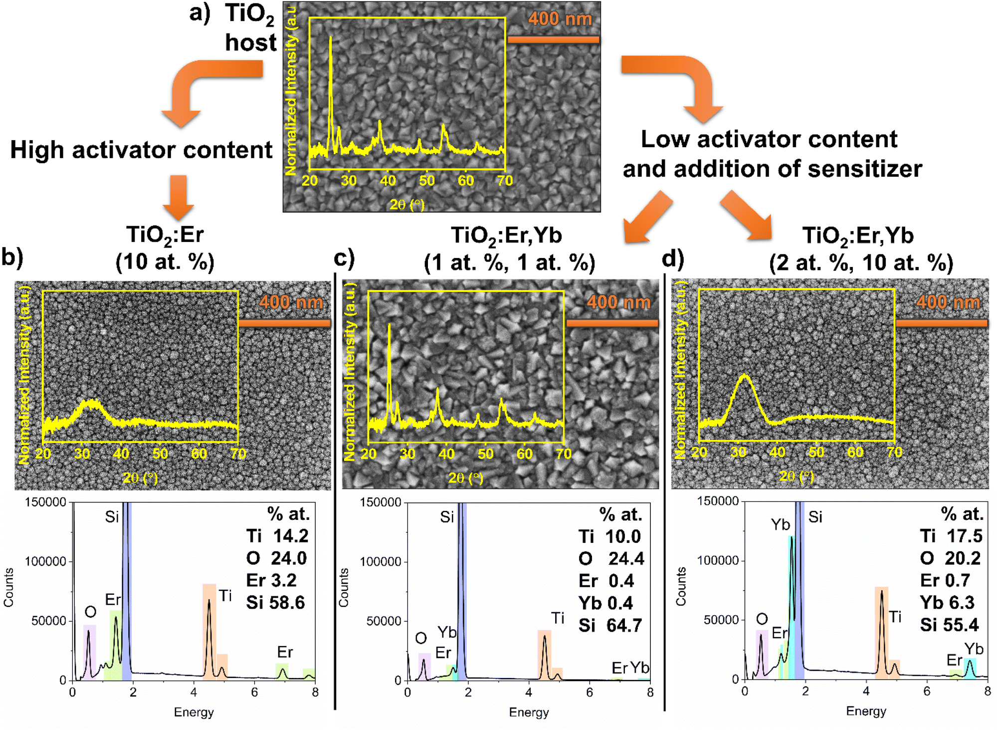 | ||
| Fig. 1 Diffractograms (GIXRD) and SEM images of (a) thin film crystallized TiO2 host, (b) modified thin film with high activator ions content TiO2:Er (10 at%), and (c and d) modified thin films with low activator content but with addition of sensitizer (c) TiO2:Er,Yb (1 at%, 1 at%), (d) TiO2:Er,Yb (2 at%, 10 at%). Additionally, EDS spectra with elemental analysis for modified thin films are presented. | ||
The presence of Er and Yb ions in films was also confirmed in the XAS measurements (Fig. 2). The absorption of synchrotron X-ray radiation in total electron yield (TEY) mode, as a very sensitive method, allowed to easily detect even very low addition of Er and Yb. The M4,5 Er and M5 Yb lines of thin films and reference oxide powders (Er2O3, Yb2O3) are presented in Fig. 2c and d. The area under the peak line in the XAS spectra collected for the same measurement sensitivity is dependent on the detected ions concentration. To compare the shape of the spectrum curves, it is necessary to perform a normalization procedure. The normalization procedure for the Ti L2,3 spectra was described in detail in our recent work,30 and here an analogous approach was applied for Ti L2,3, O K, Er M4,5 and Yb M5 spectra. The normalized Er M4,5 XAS spectra (Fig. 2c) have a similar shape, not affected by the phase composition of the samples. The same can be noticed for the normalized Yb M5 spectra (Fig. 2d). The Er M5 and M4 lines are related to 3d5/2 → 4f and 3d3/2 → 4f transitions with major absorption energies at 1404.9 and 1446.3 eV, respectively as reported in ref. 34. The collected spectra showed peak splitting of the Er M5 line into four maxima (1404, 1406, 1409, and 1411 eV), while for Er M4 one maximum at 1447 was observed. For Yb M5 only a single line was observed at 1521 eV, which can be attributed to 3d104f7/213 → 3d5/294f14 transition.34 Spectra in Fig. 2c and d insets are presented without normalization but for the same measurement sensitivity. Here, differences in the intensity of the signal are related to the amount of ions in the samples. The Ti L2,3 and O K lines are strongly affected by changes in phase composition (Fig. 2a and b). The Ti L2,3 spectrum with sharp peaks at the pre-edge, and the splitting of the L3-eg peak at 460 eV indicated a well crystalized anatase and rutile phase, while for amorphous samples the L3-eg peak splitting did not occur (inset in Fig. 2 a). For detailed analysis of Ti L2,3 lines, see ref. 30. The maxima of the O K lines at 531, 533, 539 and 544 eV can be assigned to 1s → t2g, 1s → eg, and 1s → a1g,t1u transitions (see also ref. 35). The O K line for the crystallized sample (Fig. 2b) had better split t2g, eg, a1g, and t1u peaks than the O K spectra of the amorphous films presented in the inset.
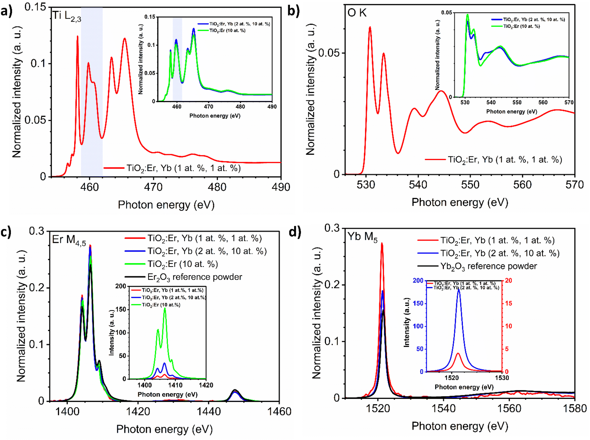 | ||
| Fig. 2 Normalized XAS spectra of: (a) Ti L2,3 and (b) O K edges of crystallized TiO2:Er,Yb thin films, in the insets amorphous TiO2:Er and TiO2:Er,Yb thin films. For the Ti L2,3 lines the L3-eg peak is marked with a light blue rectangle. XAS spectra of: (c) Er M4,5 and (d) Yb M5 edges of TiO2:Er, TiO2:Er,Yb thin films, and reference lanthanide oxide powders (Er2O3, Yb2O3). In the insets, XAS spectra of the Er M4,5 and Yb M5 edges with intensity for the same measurement sensitivity are shown. | ||
The spectral dependence of transmittance coefficient (T) (Fig. 3a) showed oscillations of transmittance in the weak absorption region, which are due to the interference in thin films. The thin film thickness ranges from 220 to 340 nm as presented in Table 1 and Fig. 3b–f. As a reference, an additional TiO2 film was used – amorphous TiO2 film deposited at room temperature, which preparation and characterization were described in detail in our recent work.36 For both TiO2 and rare earth modified TiO2 amorphous thin films, a shift of the fundamental absorption edge to higher energies in comparison to crystallized films can be observed. The absorption coefficient (α) in the strong and weak absorption region was calculated using the “envelope method” from the transmittance and reflectance spectra taking into account the values of the thin film thickness measured with the profilometer. The optical bandgap Eg can be determined from the Tauc method based on eqn (1):
| (αℏν)1/γ = A(ℏν − Eg) | (1) |
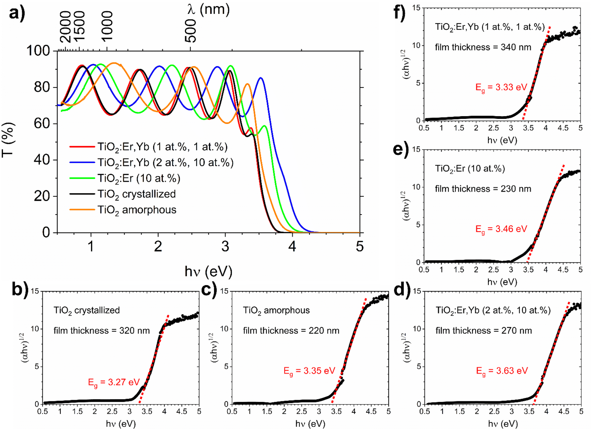 | ||
| Fig. 3 UV-VIS-NIR spectrophotometry results for TiO2, TiO2:Er, and TiO2:Er,Yb thin films. (a) Spectral dependence of the transmittance coefficient (T), (b–f) (αℏν)1/2 vs. ℏν dependence for optical bandgap Eg determination (Tauc method) with thin film thickness data from profilometer measurements. As a reference the amorphous TiO2 film results are provided. | ||
The bandgap energy for photoanode materials can be also evaluated from photoelectrochemical methods.38 For a n-type film, if film thickness Lf is very small, the photocurrent Iph and the absorption coefficient α relationship could be simplified to eqn (2):39
| Iph = eJ0αLf | (2) |
| (Iphℏν)1/γ = B(ℏν − Eg) | (3) |
| B = A(eJ0Lf)1/γ | (4) |
For TiO2 and TiO2:Er,Yb (1 at%, 1 at%) thin film photoanodes, which are samples with the best photoresponse (see results in our previous work29), this complementary method for bandgap determination based on photocurrent measurements was applied. From the photocurrent Iph versus time characteristics (Fig. 4a and b) the spectral dependence of photocurrent was determined and presented in Fig. 4c. The plots of (Iph·ℏν)1/2 versus ℏν (Fig. 4d) allow to determine bandgap value E from the intersection of the line fitted to the experimental data with the photon energy hν axis. For TiO2 and TiO2:Er,Yb thin films, bandgap value from photoelectrochemical measurements is 2.93 eV and 2.97 eV respectively. For both methods, TiO2 has slightly lower (0.04–0.05 eV) bandgap energy value than TiO2:Er,Yb (1 at%, 1 at%). The difference of about 0.3 eV between the bandgap energy evaluated from optical and photoelectrochemical measurements was also observed in other work.40
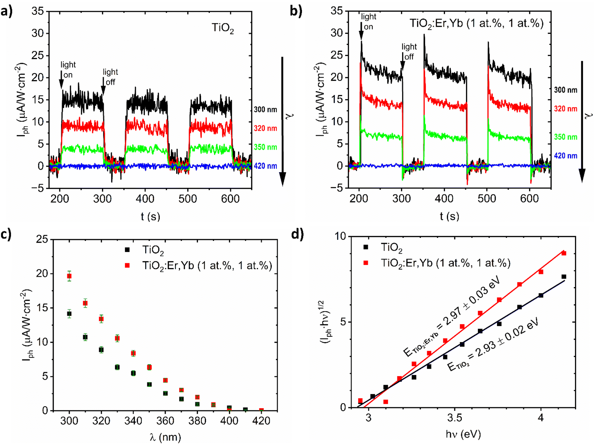 | ||
| Fig. 4 Selected characteristics of photocurrent Iph versus time (t) under monochromatic illumination (λ = 300, 320, 350, and 420 nm) for (a) crystallized TiO2 and (b) TiO2:Er,Yb (1 at%, 1 at%) thin films. (c) Spectral dependence of photocurrent Iph vs. λ, and (d) (Iph·ℏν)1/2 vs. ℏν for photoelectrochemical bandgap E determination for crystallized TiO2 and TiO2:Er,Yb (1 at%, 1 at%) thin film photoanodes. | ||
The photoluminescence spectra of crystallized and amorphous rare earth modified thin films are presented in Fig. 5a (the pure TiO2 thin film served as a reference). In this experiment, Raman and PL signals are collected at the same time, thus both TiO2 phonon bands (close to the 488 nm laser excitation line) and Er3+ emission bands (at higher wavelengths) can be observed. A similar setup for the PL measurement of Eu3+/TiO2 xerogels was described by Borlaf et al.41
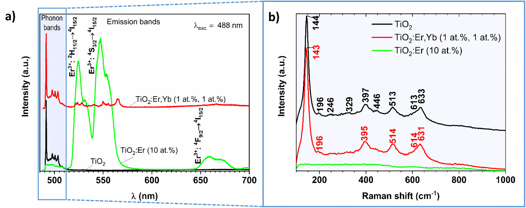 | ||
| Fig. 5 (a) Photoluminescence and (b) Raman spectra recorded for crystallized and amorphous rare earth modified TiO2 thin films and crystallized pure TiO2 reference thin film upon 488 nm laser excitation. | ||
In the phonon bands range for crystalized TiO2:Er,Yb (1 at%, 1 at%) thin film narrow lines at 490, 498, 501, and 504 nm can be observed, similarly to well-crystallized TiO2, while for amorphous TiO2:Er (10 at%) only increase in the noise level is observed. Detailed analysis of the 490–515 nm wavelength range is presented in Fig. 5b. The TiO2 phases were identified according to the following reference Raman modes: 144 (Eg), 197 (Eg), 400 (B1g), 516 (A1g + B1g) and 640 cm−1 (Eg) for anatase;42 143 (B1g), 447 (Eg), 612 (A1g), and 826 cm−1 (B2g) for rutile;43 154 (A1g), 247 (A1g), 320 (B1g), and 329 (B2g) cm−1 for brookite.44 The obtained Raman shift values compared with the reference data confirm that the crystallized samples are a mixture of anatase, rutile and brookite (Table 2). The recorded PL spectra (Fig. 5a) allowed for investigation of the luminescence properties and analysis of the optical quality of the thin film. The sample with high Er3+ activator content showed high emission in green, peaks with the main maximum at 524 and 547 nm, which corresponds to 2H11/2 → 4I15/2, and 4S3/2 → 4I15/2 transitions in Er3+ respectively, and weak emission in red with the maximum at 659 nm (4F9/2 → 4I15/2). Pure TiO2 does not exhibit additional emission peaks in the visible light range. The results of PL proved the lack of clustering within Er3+ ions and the possibility of considering thin films in energy conversion systems.
| Raman shift (cm−1) upon 488 nm laser excitation | Upconversion emission wavelength λ (nm) upon 980 nm laser excitation | |||||||
|---|---|---|---|---|---|---|---|---|
| TiO2 crystallized | TiO2:Er,Yb (1 at%, 1 at%) | Anatase42 | Rutile43 | Brookite44 | TiO2:Er,Yb (1 at%, 1 at%) | TiO2:Er,Yb (2 at%, 10 at%) | TiO2:Er (10 at%) | Transitions24,46 |
| 144 | 143 | 144 (Eg) | 143 (B1g) | 154 (A1g) | 387 | 4G11/2 → 4I15/2 | ||
| 196 | 197 (Eg) | 410 | 2H9/2 → 4I15/2 | |||||
| 246 | 247 (A1g) | 524 | 524 | 523 | 2H11/2 → 4I15/2 | |||
| 329 | 320 (B1g), 329 (B2g) | 538 | 2H11/2 → 4I15/2 | |||||
| 397 | 395 | 400 (B1g) | 551 | 546 | 545 | 4S3/2 → 4I15/2 | ||
| 446 | 447 (Eg) | 562 | 4S3/2 → 4I15/2 | |||||
| 513 | 514 | 516 (A1g + B1g) | 660 | 658 | 659 | 4F9/2 → 4I15/2 | ||
| 613 | 614 | 612 (A1g) | ||||||
| 633 | 631 | 640 (Eg) | ||||||
To analyse the upconversion properties of the photoanodes (rare earth modified TiO2 thin films on the ITO substrate), emission spectra were collected under the 980 nm laser diode excitation with laser pump power adjusted within the 100–1000 mW range (Fig. 6a–c). Measurements in a function of the pumping power confirmed the non-linear character of luminescence (Fig. 6d). All samples exhibit the main emission peak in the green wavelength range (λ ≈ 524 nm). TiO2:Er,Yb (2 at%, 10 at%) showed one order of magnitude higher green emission intensity than TiO2:Er,Yb (1 at%, 1 at%) and TiO2:Er (10 at%). The emission spectrum of the crystallized sample, similarly to the XAS spectra, has more split peaks, as presented in Table 2. The peak located at 490 nm wavelength in the UC spectra has origin from the second harmonic of the laser generated in the samples. On the basis of TiO2:Er and TiO2:Er,Yb spectra (Fig. 6a–c), it was observed that the addition of a high concentration of Yb ions significantly increases intensity of the upconversion emission. It occurs due to the following probable mechanisms45 (schematic diagram of UC processes shown in Fig. 6e):
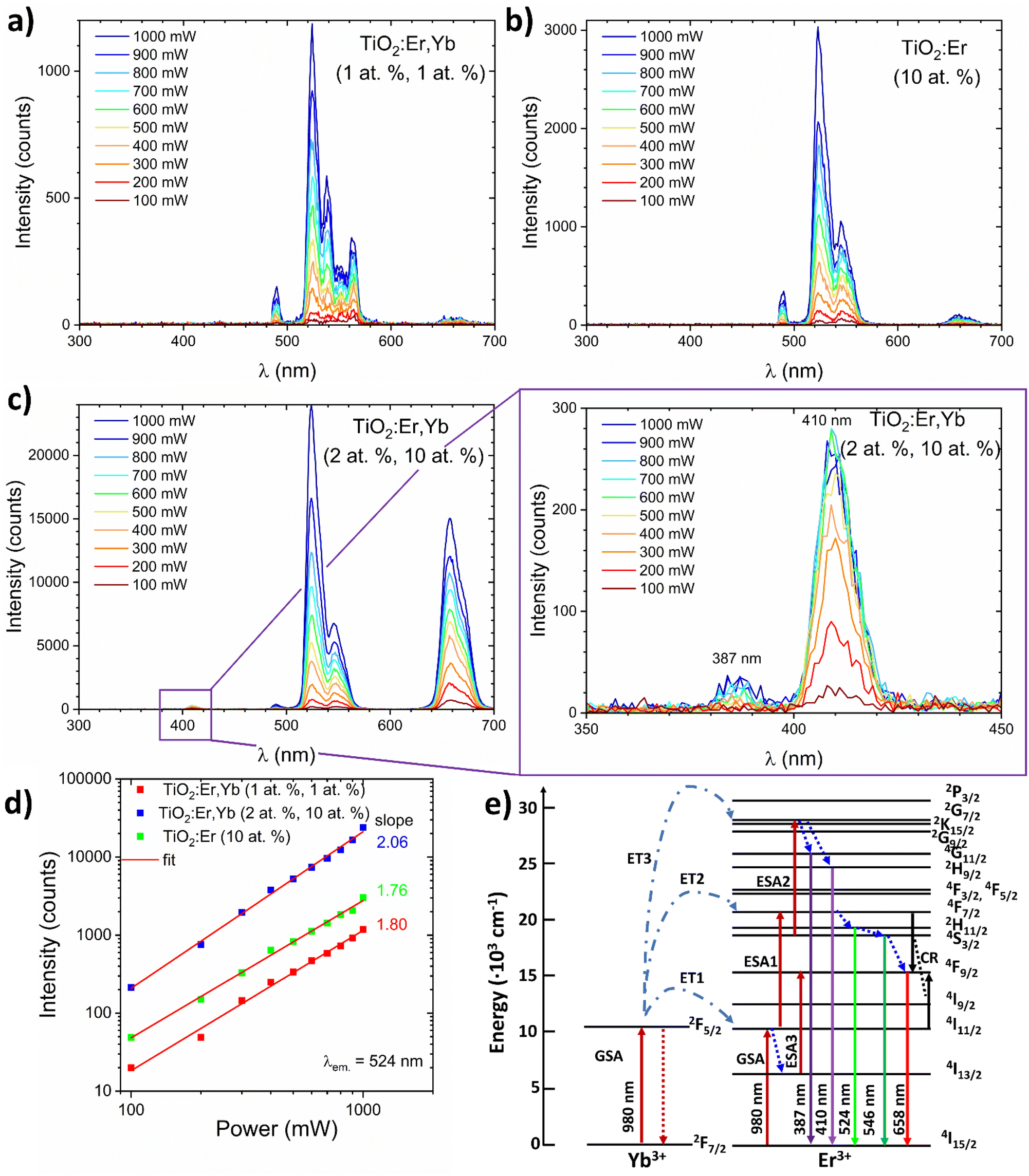 | ||
| Fig. 6 (a–c) Dependence of the upconversion spectrum of TiO2 and TiO2:Er,Yb thin films on the excitation power of the 980 nm laser diode. (d) Logarithmic plot of the green emission intensities of Er-, and Yb-modified thin films as a function of the laser pump power. (e) Upconversion transitions in a Yb3+/Er3+ couple upon 980 nm excitation. The dash and dot lines symbolize energy transfer (ET), the dote lines represent relaxation, the full lines indicate ground state absorption (GSA), excited state absorption (ESA), cross-relaxation transitions (CR) and radiative decay. | ||
(1) Due to two subsequent transfers (ET1, ET2) from ytterbium ion (2F5/2) the 4F7/2 Er3+ level is directly excited. Non-radiative relaxations from 4F7/2 Er3+ level populate the following 2H11/2, 2H11/2 and 4F9/2 levels. Then, radiative emissions at 524 nm, 546 nm and 658 nm occur as a result of transitions from 2H11/2, 2H11/2 and 4F9/2 levels to the ground state 4I15/2 respectively.
(2) Nonradiative transition 4I11/2 → 4I13/2 may promote population (LD and ET from Yb is possible) of the 4F9/2 level (ESA3) from which radiative relaxation 4F9/2 → 4I15/2 enhances emission in red.
(3) In result of high concentration, two adjacent Er3+ ions undergo a cross-relaxation according to 4F7/2 + 4I11/2 → 4F9/2 + 4F9/2 scheme (CR).
(4) In the presence of high concentration of Er, Yb (2 at%, 10 at%) the third Yb photon (ET3) may excite 4S3/2 Er ions to the 2G9/2 level. Then, after non-radiative relaxation to the 4G11/2 and 2H9/2 levels, emissions at 384 and 410 nm take place after the transition to the ground state.
In case of higher than NaYF4 phonon host like TiO2, both multi-phonon and cross-relaxation mechanisms are promoted. It is consistent with the results of log-log plots (λem = 524 nm, Fig. 6d) where the ET3 is possible only for the sample doped with 10 at% of Yb where slope exceeded 2.0 value. Increasing the total content of Ln3+ ions changes luminous centers surroundings which is indicated by the GIXRD and XAS results. Moreover, the distances between Er3+ and Yb3+ ions are reduced as the Ln3+ content increases, which increases UC probability and CR leading to enhanced UV-red emission.
Jung26 reported that the main UC emission color of TiO2:Er3+/Yb3+ phosphors is rather controlled by the Yb3+ than the concentration of Er3+ – with increasing Yb3+ ions concentration the red-to-green ratio increased significantly. Fig. 6d shows a logarithmic plot of the green emission intensities of rare earth modified thin films as a function of the laser pump power. The slope values close to 2 (2.06, 1.76, and 1.80 mW) indicate that this level is populated in two-photon process, which is in accordance with Er3+ energy diagram.9 For TiO2:Er,Yb (2 at%, 10 at%) thin film, UV (387 nm) and violet (410 nm) upconversion emission was observed (Fig. 6c inset), confirming the high efficiency of this UC material. Moreover, achieving upconversion from IR to UV is very attractive to enhance performance of TiO2 based photoanodes. Based on energy diagrams in ref. 46–48 possible mechanism of three-photon upconversion in the Yb3+ and Er3+ couple is presented in Fig. 6e and can be described as follows. After two-photon excitation from the 4I15/2 ground state to the 4F7/2 excited state, multi-phonon relaxation to 4F9/2 occurs. Absorption of third 980 nm photon allows excitation to 2G7/2, then relaxation to the 2H9/2 or 4G11/2 energy level takes place. During the 2H9/2, 4G11/2 → 4I15/2 transition 410 and 387 nm photons are emitted.
The luminescence decay profiles (Fig. 7) were measured under 980 nm excitation. The decay curves for green emission 2H11/2 → 4I15/2 (λem ≈ 525 nm) were fitted according to eqn (5):
|
I(t) = A1exp(−t/τ1) + A2exp(−t/τ2)
| (5) |
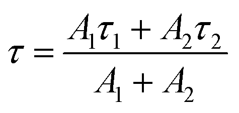 | (6) |
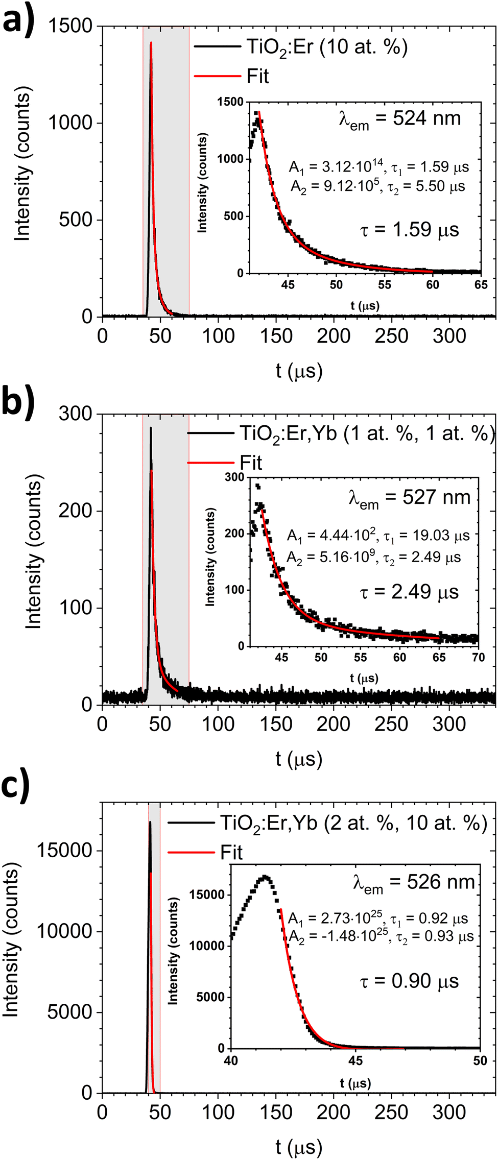 | ||
| Fig. 7 The upconversion luminescence decay for green emission (λem ≈ 525 nm) of (a) TiO2:Er and (b and c) TiO2:Er,Yb thin films upon 980 nm laser diode excitation. In the insets, results of the decay curve fitting and values of average decay time are shown. | ||
For TiO2:Er and TiO2:Er,Yb thin films, the average decay times τ of green emission were several μs (0.90–2.49 μs) as shown in Fig. 7. Lakhotiya et al.49 reported TiO2:Er thin films sputtered and annealed at 350 °C, which upon 800 nm laser excitation have a decay time of infrared emission (4I11/2 → 4I15/2 transition) around 10 μs. Zhanci et al.50 showed that the measured lifetime of the erbium ion 4S3/2 and 2H11/2 states in oxyfluoride tellurite glass at 303 K is approximately 20 μs.
Conclusions
The thin film with small addition of activator and sensitizer TiO2:Er,Yb (1 at%, 1 at%) was a well-crystallized mixture of anatase, rutile and brookite, similarly to pure TiO2, while the high addition of activator or sensitizer ions in TiO2:Er (10 at%) and TiO2:Er,Yb (2 at%, 10 at%) thin films led to amorphization as it was evaluated from GIXRD and XAS measurements. EDS and XAS measurements confirmed that erbium (activator) and ytterbium (sensitizer) ions were introduced into the TiO2 host. The TiO2:Er and TiO2:Er,Yb thin films deposited in the magnetron sputtering process showed upconversion from NIR to VIS with main emission in green (λem ≈ 525 nm). Both TiO2:Er,Yb (1 at%, 1 at%) and TiO2:Er (10 at%) showed weak emission in red (λem ≈ 660 nm), while for TiO2:Er,Yb (2 at%, 10 at%) thin film increased red emission and even upconversion from NIR to UV was observed. Thus, it can be concluded that the higher content of activator and sensitizer allowed for more efficient upconversion, and the thin film ability to upconvert NIR photons was not affected negatively by the amorphization. Both UC spectra and XAS spectra (Ti L2,3 and O K edges) are more split for crystallized samples than for amorphous ones. The emission spectrum depends not only on the host type but also on the activator and sensitizer ions surroundings. As shown in XAS spectra, samples with high erbium (10 at%) and ytterbium (10 at%) content have different surroundings than sample with low Er and Yb addition. It has an impact on the average decay times of green emission. The average decay time of a several μs (typical for the TiO2 host) decreases with increasing total Ln3+ content from 2.49, through 1.59 to 0.90 μs. Further optimalization of thin film composition, structure, microstructure, and optical properties to achieve high upconversion from NIR to UV and to maintain high photoelectrochemical performance is crucial for the development of efficient upconverting TiO2 photoanodes for photoelectrochemical water splitting.Conflicts of interest
There are no conflicts to declare.Acknowledgements
AŚ has been partly supported by the EU Project POWR.03.02.00–00-I004/16. The research was financed by NCN Poland, decision no. UMO-2020/37/B/ST8/02539. X-ray absorption experiment entitled “Local atomic structure of up-converting Ti(Er,Yb)O2 thin film photoelectrodes for hydrogen evolution” (no. 211047) was performed at PIRX beamline of National Synchrotron Radiation Centre SOLARIS, the access to which was provided by the project of Polish Ministry of Education and Science under contract no. 1/SOL/2021/2.Notes and references
- Y. Zhang and J. He, Phys. Chem. Chem. Phys., 2015, 17, 20154–20159 RSC.
- J. Zhou, Q. Liu, W. Feng, Y. Sun and F. Li, Chem. Rev., 2015, 115, 395–465 CrossRef CAS.
- H. Dong, L. D. Sun and C. H. Yan, J. Am. Chem. Soc., 2021, 143, 20546–20561 CrossRef CAS PubMed.
- M. K. Hossain, M. H. Ahmed, M. I. Khan, M. S. Miah and S. Hossain, ACS Appl. Electron. Mater., 2021, 3, 4255–4283 CrossRef CAS.
- P. Dawson and M. Romanowski, J. Lumin., 2020, 222, 117143 CrossRef CAS.
- J. De Wild, A. Meijerink, J. K. Rath, W. G. J. H. M. Van Sark and R. E. I. Schropp, Energy Environ. Sci., 2011, 4, 4835–4848 RSC.
- P. Zhang, L. Liang and X. Liu, J. Mater. Chem. C, 2021, 9, 16110–16131 RSC.
- Q. Tian, W. Yao, W. Wu and C. Jiang, Nanoscale Horiz., 2019, 4, 10–25 RSC.
- G. Gorni, J. J. Velázquez, M. Kochanowicz, D. Dorosz, R. Balda, J. Fernández, A. Durán and M. J. Pascual, RSC Adv., 2019, 9, 31699–31707 RSC.
- Z. Qiu, J. Shu and D. Tang, Anal. Chem., 2018, 90, 1021–1028 CrossRef CAS PubMed.
- F. Zhang, in Photon Upconversion Nanomaterials: Nanostructure Science and Technology, ed. D. J. Lockwood, Springer, Berlin, Heidelberg, 2015, pp. 1–20 Search PubMed.
- K. K. Markose, R. Anjana and M. K. Jayaraj, in Nanostructured Metal Oxides and Devices: Optical and Electrical properties, ed. M. K. Jayaraj, Springer Nature, Singapore, 2020, pp. 47–102 Search PubMed.
- M. K. Mahata, H. C. Hofsäss and U. Vetter, in Luminescence, ed. J. Thirumalai, InTech, Rijeka, 2016, pp. 109–131 Search PubMed.
- F. Auzel, Chem. Rev., 2004, 104, 139–173 CrossRef CAS PubMed.
- A. Nadort, J. Zhao and E. M. Goldys, Nanoscale, 2016, 8, 13099–13130 RSC.
- M. Radecka, A. Kusior, A. Trenczek-Zając and K. Zakrzewska, in Advances in Inorganic Chemistry, ed. R. van Eldik and W. Macyk, Academic Press, Cambridge, Massachusetts, 2018, vol. 72, pp. 145–183 Search PubMed.
- L. Jiang, S. Zhou, J. Yang, H. Wang, H. Yu, H. Chen, Y. Zhao, X. Yuan, W. Chu and H. Li, Adv. Funct. Mater., 2022, 32, 2108977 CrossRef CAS.
- J. Wang, Z. Wang, W. Wang, Y. Wang, X. Hu, J. Liu, X. Gong, W. Miao, L. Ding, X. Li and J. Tang, Nanoscale, 2022, 14, 6709–6734 RSC.
- T. S. Atabaev and A. Molkenova, Front. Mater. Sci., 2019, 13, 335–341 CrossRef.
- E. Cerrato, E. Gaggero, P. Calza and M. C. Paganini, Chem. Eng. J. Adv., 2022, 10, 100268 CrossRef CAS.
- J. Zhang, X. Wang, W.-T. Zheng, X.-G. Kong, Y.-J. Sun and X. Wang, Mater. Lett., 2007, 61, 1658–1661 CrossRef CAS.
- W. A. Pisarski, K. Kowalska, M. Kuwik, J. Pisarska, J. Dorosz, J. Żmojda, M. Kochanowicz and D. Dorosz, Opt. Mater. Express, 2022, 12, 2912 CrossRef CAS.
- R. Salhi and J.-L. Deschanvres, J. Lumin., 2016, 176, 250–259 CrossRef CAS.
- J. A. B. Pérez, M. Courel, R. C. Valderrama, I. Hernández, M. Pal, F. P. Delgado and N. R. Mathews, Vacuum, 2019, 169, 108873 CrossRef.
- S. R. Johannsen, S. Roesgaard, B. Julsgaard, R. A. S. Ferreira, J. Chevallier, P. Balling, S. K. Ram and A. N. Larsen, Opt. Mater. Express, 2016, 6, 1664–1678 CrossRef CAS.
- K. Y. Jung, RSC Adv., 2020, 10, 16323–16329 RSC.
- A. Kot, D. Dorosz, M. Radecka and K. Zakrzewska, Int. J. Hydrogen Energy, 2021, 46, 12082–12094 CrossRef CAS.
- A. Kot, M. Radecka, D. Dorosz and K. Zakrzewska, Materials, 2021, 14, 4085 CrossRef CAS PubMed.
- A. Kot, M. Radecka and K. Zakrzewska, Appl. Surf. Sci., 2023, 608, 155127 CrossRef CAS.
- K. Płacheta, A. Kot, J. Banas-Gac, M. Zając, M. Sikora, M. Radecka and K. Zakrzewska, Appl. Surf. Sci., 2023, 608, 155046 CrossRef.
- A. Bahtat, M. Bouderbala, M. Bahtat, M. Bouazaoui, J. Mugnier and M. Druetta, Thin Solid Films, 1998, 323, 59–62 CrossRef CAS.
- J. Reszczyńska, T. Grzyb, J. W. Sobczak, W. Lisowski, M. Gazda, B. Ohtani and A. Zaleska, Appl. Catal., B, 2015, 163, 40–49 CrossRef.
- J. A. B. Pérez, M. Courel, M. Pal, F. P. Delgado and N. R. Mathews, Ceram. Int., 2017, 43, 15777–15784 CrossRef.
- B. T. Thole, G. van der Laan, J. C. Fuggle, G. A. Sawatzky, R. C. Karnatak and J.-M. Esteva, Phys. Rev. B: Condens. Matter Mater. Phys., 1985, 32, 5107–5118 CrossRef CAS PubMed.
- M. A. van Spronsen, X. Zhao, M. Jaugstetter, C. Escudero, T. Duchoň, A. Hunt, I. Waluyo, P. Yang, K. Tschulik and M. B. Salmeron, J. Phys. Chem. Lett., 2021, 12, 10212–10217 CrossRef CAS PubMed.
- J. Banas-Gac, M. Radecka, A. Czapla, E. Kusior and K. Zakrzewska, Appl. Surf. Sci., 2023, 616, 156394 CrossRef CAS.
- P. Makuła, M. Pacia and W. Macyk, J. Phys. Chem. Lett., 2018, 9, 6814–6817 CrossRef PubMed.
- J. Sar, K. Kołodziejak, K. Wysmułek, K. Orliński, A. Kusior, M. Radecka, A. Trenczek-Zając, K. Zakrzewska and D. A. Pawlak, in Photo-Electrochemical Solar Cells, ed. N. D. Sankir and M. Sankir, Wiley, 2019, pp. 305–347 Search PubMed.
- S. A. Campbell, L. M. Peter and J. S. Buchanan, J. Power Sources, 1992, 40, 137–146 CrossRef CAS.
- M. Radecka, A. Trenczek-Zajac, K. Zakrzewska and M. Rekas, J. Power Sources, 2007, 173, 816–821 CrossRef CAS.
- M. Borlaf, M. T. Colomer, R. Moreno and A. De Andrés, J. Am. Ceram. Soc., 2015, 98, 338–345 CrossRef CAS.
- T. Ohsaka, F. Izumi and Y. Fujiki, J. Raman Spectrosc., 1978, 7, 321–324 CrossRef.
- S. P. S. Porto, P. A. Fleury and T. C. Damen, Phys. Rev., 1967, 154, 522–526 CrossRef CAS.
- G. A. Tompsett, G. A. Bowmaker, R. P. Cooney, J. B. Metson, K. A. Rodgers and J. M. Seakins, J. Raman Spectrosc., 1995, 26, 57–62 CrossRef CAS.
- Y. Wu, S. Lin, J. Liu, Y. Ji, J. Xu, L. Xu and K. Chen, Opt. Express, 2017, 25, 22648 CrossRef CAS PubMed.
- R. K. Tamrakar, D. P. Bisen and N. Bramhe, Luminescence, 2015, 30, 668–676 CrossRef CAS PubMed.
- W. G. J. H. M. van Sark, J. de Wild, J. K. Rath, A. Meijerink and R. E. I. Schropp, Nanoscale Res. Lett., 2013, 8, 1–10 CrossRef PubMed.
- K. K. Markose, R. Anjana, A. Antony and M. K. Jayaraj, J. Lumin., 2018, 204, 448–456 CrossRef CAS.
- H. Lakhotiya, J. Christiansen, J. L. Hansen, P. Balling and B. Julsgaard, J. Appl. Phys., 2018, 124, 163105 CrossRef.
- Y. Zhanci, H. Shihua, L. Shaozhe and C. Baojiu, J. Non-Cryst. Solids, 2004, 343, 154–158 CrossRef CAS.
| This journal is © The Royal Society of Chemistry 2023 |