
 Open Access Article
 This Open Access Article is licensed under a Creative Commons Attribution-Non Commercial 3.0 Unported Licence
First-principles study on electronic states of In2Se3/Au heterostructure controlled by strain engineering†
Sha Hanabc,
Cai-Juan Xia*abc,
Min Liabc,
Xu-Mei Zhaoabc,
Guo-Qing Zhangabc,
Lian-Bi Liabc,
Yao-Heng Suabc and
Qing-Long Fang *abc
*abc
aSchool of Science, Xi'an Polytechnic University, Xi'an 710048, Shaanxi, China. E-mail: caijuanxia@xpu.edu.cn; qinglong_fang@xpu.edu.cn
bEngineering Research Center of Flexible Radiation Protection Technology, University of Shaanxi Province, Xi'an Polytechnic University, Xi'an 710048, Shaanxi, China
cXi'an Key Laboratory of Nuclear Protection Textile Equipment Technology, Xi'an Polytechnic University, Xi'an 710048, Shaanxi, China
First published on 11th April 2023
Abstract
The development of low-dimensional multifunctional devices has become increasingly important as the size of field-effect transistors decreases. In recent years, the two-dimensional (2D) semiconductor In2Se3 has emerged as a promising candidate for applications in the fields of electronics and optoelectronics owing to its remarkable spontaneous polarization properties. Through first-principles calculations, the effects of the polarization direction and biaxial tensile strain on the electronic and contact properties of In2Se3/Au heterostructures are investigated. The contact type of In2Se3/Au heterostructures depends on the polarization direction of In2Se3. The more charge transfers from the metal to the space charge region, the biaxial tensile strain increases. Moreover, the upward polarized In2Se3 in contact with Au maintains a constant n-type Schottky contact as the biaxial tensile strain increases, with a barrier height ΦSB,n of only 0.086 eV at 6% strain, which is close to ohmic contact. On the other hand, the downward polarized In2Se3 in contact with Au can be transformed from p-type to n-type by applying a biaxial tensile strain. Our calculation results can provide a reference for the design and fabrication of In2Se3-based field effect transistors.
1. Introduction
As the miniaturization of silicon-based field-effect transistors (FETs) progresses, their scalability is approaching its limit, and a critical factor limiting this scalability is the short-channel effect. Therefore, an alternative material to silicon should be developed to avoid those scaling issues in future logic transistor applications. Two-dimensional (2D) materials, such as transition metal dichalcogenides (TMDs) and black phosphorus (BP), with atomic thickness, dangling-bond-free surface, and a moderate band gap of Eg ∼ 1–2 eV, are active candidates for application in logic transistors.1–4 However, TMDs suffer from a low carrier mobility (∼200 cm2 V−1 s−1), and BP easily decomposes in air, and thus they are unsuitable for high-performance applications.5,6 In recent years, In2Se3 has attracted much attention as an emerging 2D III-VI semiconductor material. This material exhibits several phases: α, β, γ, δ, and κ, depending on the temperature and preparation conditions.7,8 Among them, α-In2Se3, which belongs to the R3m group (rhombohedral structure), is stable at room temperature.9 From bulk to monolayer, α-In2Se3 has a direct band gap of 1.45 eV to 2.8 eV, comparable to BP.10 It is theoretically predicted that the electron (hole) carrier mobility of monolayer α-In2Se3 is as high as 920–960 (510–560) cm2 V−1 s−1.11 In 2D In2Se3-based FET, a high on-off ratio exceeding 108 and on-state current of 671 μA μm−1 have been observed.12 In addition, Ding et al.13 have theoretically predicted the existence of in-plane and out-of-plane ferroelectricity of the monolayer In2Se3 at room temperature and subsequently demonstrated the ferroelectricity of the material experimentally.14,15 Xue et al. observed ferroelectric polarization switching and hysteresis loop sown to the bilayer and monolayer In2Se3 at room temperature, indicating that ferroelectricity of the thinnest layer can be realized in 2D materials.16 More recently, Wan et al. successfully fabricated a 2D ferroelectric FET consisting of graphene and layered In2Se3, demonstrating nonvolatile memory after repeated writing of more than 105 cycles.17 Wang et al. observed the abnormal bipolar resistive switching phenomenon in In2Se3-based FET, which was rationalized on the basis of Schottky barrier (SB) modulation by in-plane ferroelectric switching.18 Thus, the presence of out-of-plane and in-plane piezoelectricity in α-In2Se3 flakes offers an opportunity for the development of both directed and non-directed piezoelectric devices, including optoelectronic devices,19–21 ferroelectric diodes, and nonvolatile memories.22In 2D FET devices with 2D semiconductor as the channel materials, contacts with metal electrodes are absolutely necessary, where SB is usually formed. The SB can induce an extra contact resistance and thus decrease the carrier transfer efficiency between the 2D semiconductor and metal electrodes, which often significantly reduces the performance of the FETs.23,24 Yang et al. theoretically predicted the formation of lateral p-type Schottky contact in monolayer In2Se3/Au heterostructure with Schottky barrier height (SBH) of 0.35 eV and 0.31 eV, respectively, using the work function approximation and quantum transport simulation methods.25 Unfortunately, the average pinning factor calculated for monolayer In2Se3 is about 0.09, which implies strong Fermi level pinning (FLP) effects.26 The robust FLP is influenced by the interplay between the metal and In2Se3 while being insensitive to the metal work function. Therefore, tuning SBH is difficult with different metal electrodes. In recent years, many methods have been proposed to tune the interfacial SBH, such as passivating the metal surface with external atoms or inserting an h-BN insulating layer between MoS2 and metal to reduce FLP, while the electron injection is impeded by a significant tunneling barrier due to the weak interaction between the 2D material and the metal layer.27–29 Strain engineering is one of the most feasible ways to tune the electronic properties of 2D heterostructures. For example, Dai et al. reported that biaxial strain could induce the band alignment of PtS2/MoTe2 and GaN/WS2 heterostructures transition from type-II to type-I but also can realize semiconductor–metal transition.30,31 The calculated carrier mobility of the CdS/SiI2 heterostructure is up to 103 cm2 V−1 s−1 by applying a biaxial strain, implying an excellent photocatalyst performance.32 Feng et al. achieved a strain sensor made of patterned α-In2Se3 films with high sensitivity (gauge factor ∼237 in −0.39% to 0.39% uniaxial strain range along the device channel length) and high spatial resolution of the strain distribution.33 Hou et al. deposited Au electrodes on α-In2Se3 nanosheets to prepare a flexible transistor, and they modulated the photoresponse characteristics of the transistor by applying plane strain and found that the optimized photoresponsiveness was improved by 200% at a compressive strain of −0.15%.34 However, the influence of strain on the electronic structures and contact properties of In2Se3/metal heterostructures are still veiled.
In this paper, the effect of biaxial strain on the interfacial electronic states and contact properties of monolayer In2Se3/Au heterostructures are investigated by first-principles calculations. Both polarization directions (upward and downward, defined by the built-in electric field) are considered. It is found that the type of contact between In2Se3 and Au depends on the polarization direction of In2Se3 contacted with Au, potentially leading to a transition from n-type to p-type behavior. Furthermore, biaxial strain engineering is a valuable method to modulate the electronic structure and contact properties of the In2Se3/Au heterostructure. This investigation offers a deeper comprehension of the interplay between strain engineering and polarization direction dependence on the interfacial properties of In2Se3/Au, presenting guidance for future In2Se3-based transistors.
2. Computational details
All calculations are performed using the Vienna ab initio simulation package (VASP) based on density functional theory.35,36 The electron-ion core interaction is described by projector augmented wave potentials, which is more precise than ultra-soft pseudo-potentials.37 For the generalized gradient approximation (GGA), not only the spatial distribution of the charge density but also the effect of the charge density gradient on the exchange correlation energy is taken into account. As we all know, the GGA approximation often underestimates the band gap of the semiconductor. However, considering the consistency of the resulting trend between the different methods, the GGA method is used in this work. The Perdew–Burke–Ernzerhof (PBE) formulation of the GGA is used to describe the exchange–correlation interaction.38 The DFT-D2 method in the Grimme scheme is employed to include the contribution of van der Waals interaction between layers.39 The cutoff energy of the plane wave is chosen to be 400 eV, and the Gaussian trailing method with an energy spread of 0.05 eV is used. The K points in the first Brillouin zone are optimized for geometry structure and static calculation using 5 × 5 × 1 and 11 × 11 × 1 grids, respectively. The ions are relaxed to the ground state using a conjugate gradient algorithm with an energy convergence rate of 1.0 × 10⁻⁵ eV and a force convergence rate of 0.02 eV Å−1 for each ion. A vacuum layer of 15 Å thickness is added in the z-direction of the lattice to avoid interactions between adjacent plates.The crystal structure of monolayer In2Se3 consists of five triangular atomic planes stacked in a sequence of Se–In–Se–In–Se. The optimized lattice constants of In2Se3 is 3.986 Å, in agreement with the experimental value of 4.0 Å.40 The polarization direction of In2Se3 is defined by the direction of the inducted built-in electric field. Both upward (left, Up-In2Se3/Au) and downward directions (right, Dw-In2Se3/Au) are studied interfacial systems, as presented in Fig. 1(a). Previous studies have demonstrated that even a few percentage modification of the in-plane lattice constants of closely aligned metal surfaces results in negligible changes in their electronic properties.41–43 However, modifying the lattice constant of In2Se3 can lead to significant changes in its electronic properties.44 Hence, in order to preserve the intrinsic properties of In2Se3, we kept the lattice size constant and followed the method described in the literature45 for our modeling. In this paper, the In2Se3/Au heterostructure is constructed by stretching the 4 × 4 supercell of Au (111) surface and matching the 3 × 3 supercell of the monolayer In2Se3 with a lattice mismatch rate of 2.610%. We maintained the minimum unit lattice constant of In2Se3 at a value of 3.9954 Å and the initial minimum unit lattice constant of Au at a value of 2.884 Å to ensure the desired structure. During the ionic relaxation of the interface structure, all atoms are completely relaxed. To investigate the effect of strain on the electronic properties of In2Se3/Au heterostructure, the In2Se3/Au heterostructure under biaxial tensile strain in the xy-plane is investigated. The biaxial tensile strain is applied along the xy-plane by varying the lattice constant of the heterostructure and can be defined as ε = (a − a0)/a0, where a0 and a are the in-plane lattice constants of the equilibrium and strained lattice constant, respectively, as shown in Fig. 1(b).
 | ||
| Fig. 1 (a) The initial configuration of the monolayer In2Se3/metal heterostructure system in both the upward and downward directions of In2Se3 (Up-In2Se3/Au and Dw-In2Se3/Au). (b) In-plane biaxial tensile strain is depicted. | ||
3. Results and discussion
As shown in Table 1, the interlayer distance (dz) is the average distance between the closest layer of In2Se3 and metal in the vertical direction. dSe–Au is set as the minimum distance between the selenium atoms in the In2Se3 layer and the atoms in the metal layer. The binding energy (Eb) is defined to evaluate the thermodynamic stability of the In2Se3/Au heterostructure as follows:| Eb = (EIn2Se3 + EAu − EIn2Se3–Au)/N, | (1) |
| 0% | 2% | 4% | 6% | 7% | ||
|---|---|---|---|---|---|---|
| Up-In2Se3/Au | dz (Å) | 2.523 | 2.478 | 2.416 | 2.348 | 2.352 |
| 2.760 (ref. 25) | ||||||
| 2.275 (ref. 46) | ||||||
| dSe–Au (Å) | 2.643 | 2.595 | 2.552 | 2.524 | 2.512 | |
| 3.340 (ref. 25) | ||||||
| Eb (eV) | 0.962 | 0.852 | 0.548 | 0.131 | −0.102 | |
| 0.510 (ref. 25) | ||||||
| Δρ (e) | 0.637 | 0.786 | 0.868 | 0.940 | 0.966 | |
| Dw-In2Se3/Au | dz (Å) | 2.665 | 2.614 | 2.551 | 2.490 | 2.464 |
| 2.920 (ref. 25) | ||||||
| 2.485 (ref. 46) | ||||||
| dSe–Au (Å) | 2.697 | 2.649 | 2.611 | 2.567 | 2.552 | |
| 3.400 (ref. 25) | ||||||
| Eb (eV) | 0.822 | 0.704 | 0.388 | 0.052 | −0.297 | |
| 0.350 (ref. 25) | ||||||
| Δρ (e) | 0.503 | 0.590 | 0.674 | 0.755 | 0.791 | |
For Up-In2Se3/Au heterostructure, dz (dSe–Au) is smaller than that of the Dw-In2Se3/Au heterostructure without strain, indicating the stronger interaction between In2Se3 and Au in Up-In2Se3/Au heterostructure, which is consistent with the literature results.25 By applying the biaxial tensile strain from 1% to 7%, the dz (dSe–Au) in both Up-In2Se3/Au and Dw-In2Se3/Au heterostructures gradually decreased, indicating a gradually enhanced interaction between In2Se3 and Au. The binding energy of the Up-In2Se3/Au heterostructure is larger than that of the Dw-In2Se3/Au heterostructure without strain. For the Up-In2Se3/Au and Dw-In2Se3/Au heterostructures, Eb gradually decreases as the biaxial tensile strain increases from 1% to 7%, reaching negative values at 7% strain, and the heterostructure changes from a stable to an unstable structure. Therefore, the later section focuses on the interfacial properties of In2Se3/Au stable structures at 1–6% strain.
To gain further insight into bonding properties and interlayer interactions, the plane-averaged charge density difference is calculated as follows:
| Δρ = ρIn2Se3–Au − ρAu − ρIn2Se3, | (2) |
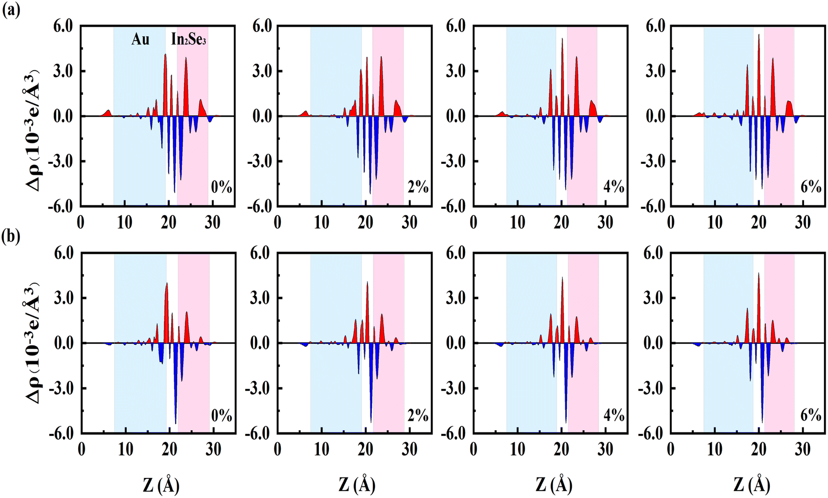 | ||
| Fig. 2 Planar average charge density difference Δρ along the z-direction of (a) Up-In2Se3/Au and (b) Dw-In2Se3/Au heterostructures under biaxial strain. Red and blue represent the accumulation and depletion of electrons, respectively. | ||
The tunneling barrier is an important factor in determining the performance of the semiconductor/metal contact. The strong interaction not only leads to high orbital overlap but also promotes the electron injection between the metal and the semiconductor, leading to the tunneling and Schottky barriers being lowered. To evaluate the tunneling barrier, the effective potential energy of In2Se3–Au with the biaxial tensile strain is calculated. The barrier width d is defined as the width of the vdW gap between Au and In2Se3, and as shown in Fig. 3, is equal to the interlayer distance dSe-M in the above-mentioned structural optimization structure. The tunneling barrier height (ΦTB,eff) is defined as the minimum barrier height that electrons need to overcome upon injection between the metal and semiconductor. According to the method in the literature,48 we can obtain:
 | (3) |
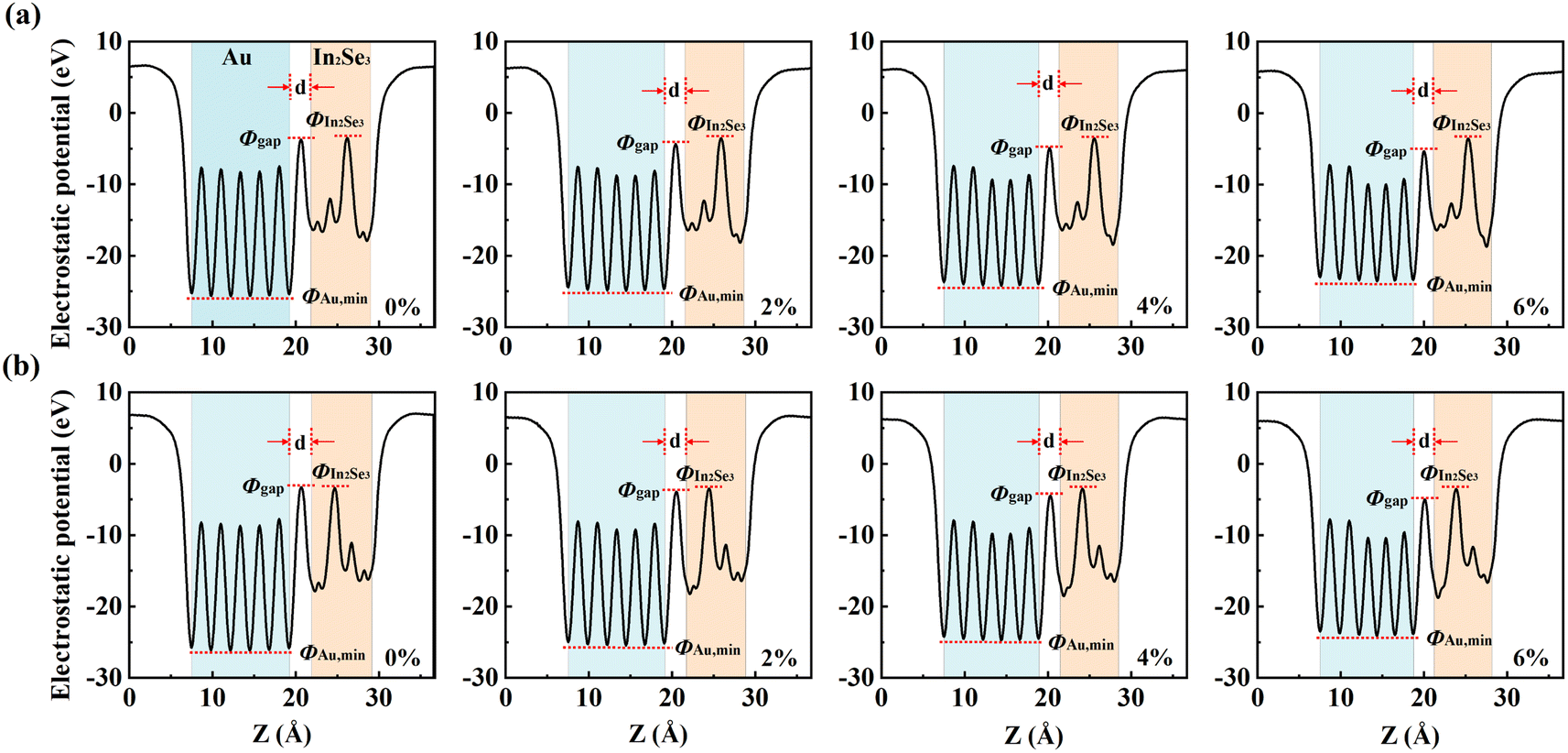 | ||
| Fig. 3 Effective potential (Veff) along the z direction (direction perpendicular to the interface) at the interface of (a) Up-In2Se3/Au and (b) Dw-In2Se3/Au contact under biaxial tensile strain. ΦIn2Se3, Φgap and ΦAu,min are the Veff of In2Se3, the vdW gap between Au and In2Se3 layers, and the minimum Veff of Au, respectively. ΦTB,eff is the height of the tunnel barrier, and d is the width of the vdW gap between Au and In2Se3. | ||
The unconstrained monolayer In2Se3 has an indirect band gap of 0.843 eV, with the valence band maximum (VBM) located between the Γ point and the M point, while the conduction band minimum (CBM) is located at the Γ point in the first Brillouin zone, which is consistent with previous theoretical results,25 as shown in Fig. S1.† Fig. 4 presents the energy band structures of (a) Up-In2Se3/Au and (b) Dw-In2Se3/Au heterostructures under biaxial tensile strain. Compared to pristine In2Se3, the energy bands of In2Se3 hybridize to some extent with Au metal, but most of the In2Se3 energy bands and Au energy bands can still be distinguished by their different colors. Blue and gray colors indicate the contributions from the In2Se3 and Au layers, respectively. It can be found that the Up-In2Se3 energy band structure is significantly more hybridized than Dw-In2Se3, and the energy band exhibits more hybridization intensity with increasing tensile strain, consistent with the strong interfacial forces discussed previously. In addition, the dispersion of CBM becomes larger with increasing tensile strain, leading to a decrease in the effective mass that is beneficial for device application.
 | ||
| Fig. 4 Band structure of In2Se3 in (a) Up-In2Se3/Au and (b) Dw-In2Se3/Au contact systems under biaxial tensile strain. The gray line indicates the energy band structure of the interfacial system. The blue line indicates the energy band structure of the ML In2Se3 projection, whose weight is represented by the size of the dot. The Fermi level is set to zero energy and is denoted by the dashed line. | ||
Fig. 5 shows the partial density of states (PDOS) of (a) Up-In2Se3/Au and (b) Dw-In2Se3/Au heterostructures under biaxial tensile strain. The conduction band portion of bulk In2Se3 is mainly contributed by In s and In p, while the valence band portion is mainly contributed by In p and Se s. Compared with pristine In2Se3, the EF of the free Up-In2Se3/Au heterostructure is shifted in the direction of the conduction band, but the EF of the free Dw-In2Se3/Au heterostructure is shifted in the direction of the valence band. Under biaxial stretching at 6% strain, the conduction band of pristine In2Se3 approaches the Fermi level while retaining its semiconductor properties, as shown in Fig. S2.† Similarly, the semiconductor properties of both Up- and Dw-In2Se3/Au heterostructures remain unchanged under biaxial stretching. Meanwhile, under biaxial tensile strain, the total electronic states of the Up-/Dw-In2Se3/Au heterostructure are gradually shifted to the left, indicating that the relative height between the CBM and the Fermi level in the In2Se3 layer can be continuously changed.
 | ||
| Fig. 5 Partial density of states (PDOS) of In2Se3 in (a) Up-In2Se3/Au and (b) Dw-In2Se3/Au contact systems under biaxial tensile strain. The black, purple, green, red, and blue lines represent the In s, In p, Se s, Se p, and the total density of states, respectively. The black vertical dashed line represents the Fermi level. | ||
The In2Se3/Au heterostructure acts as a metal–semiconductor contact heterostructure, and the Fermi level of the combined system is located in the In2Se3 band gap region, resulting in the formation of a Schottky barrier at the interface. There are two ways to calculate SBH, one is Mott–Schottky estimation, and the other is first-principles calculation. The Mott–Schottky estimation is based on ignoring the interaction between the metal and semiconductor, defining n-type SBH as the difference between the metal work function ΦM and the electron affinity of In2Se3 χIn2Se3, where ΦM is the difference between the vacuum potential and the Fermi level, and χIn2Se3 is the free energy difference between the conduction band minimum (CBM) level and the vacuum electron level. The work function of Au (111) is calculated to be 5.152 eV. Owing to the asymmetric structure of In2Se3 and the built-in electric field caused by spontaneous ferroelectric polarization along the vertical direction, the work functions on its two sides are different. The calculated χIn2Se3 of Up-In2Se3 is 5.111 eV, while the χIn2Se3 of Dw-In2Se3 is 4.613 eV. It can be found that an n-type Schottky contact is formed between Au and Up-In2Se3 with an electronic SBH of 0.041 eV. It forms a lateral p-type Schottky barrier for Dw-In2Se3 contacted with Au and the SBH of 0.251 eV. In first-principles calculations, the n-type Schottky barrier (ΦSB,n) is indeed the energy difference of the conduction band minimum (CBM) with respect to EF, while the p-type Schottky barrier (ΦSB,p) is indeed the energy difference of the valence band maximum (VBM) with respect to EF. It can be found that the polarization direction of In2Se3 is upward, and the In2Se3/Au heterostructure presents an n-type Schottky contact with ΦSB,n = 0.410 eV under no strain. On the contrary, when the polarization direction of In2Se3 is downward, the contact type between Au and In2Se3 becomes a p-type Schottky contact with ΦSB,p = 0.093 eV. The large difference in the values of SBH calculated by the two methods reflects the possible existence of Fermi level pinning (FLP) behavior at the interface.
Fig. 6 displays the SBH results of Schottky–Mott estimates and first-principles calculations. The strain dependence of SBH estimated by the Schottky–Mott limit is determined by the strain dependence of intrinsic properties of Au and In2Se3. The SBH of In2Se3/Au heterostructure is found to decrease as the work function of Au decreases, and the electron affinity of In2Se3 increases under tensile strain. The contribution of interfacial atomic and electronic rearrangements to the SBH is completely ignored. However, when the tensile strain reaches 6%, the SBH of the Up-In2Se3/Au heterostructure becomes 0.086 eV by using the first-principles calculations, which is close to ohmic contact. The electrons in the Au layer can freely flow to the In2Se3 layer through the In2Se3/Au contact. However, the VBM of Dw-In2Se3/Au heterostructure is gradually moved away from the Fermi level under the action of biaxial tensile strain, resulting in a gradual increase of the SBH at the interface. Until 6% tensile strain, Dw-In2Se3/Au heterostructure changes from p-type to n-type Schottky barrier. Our findings suggest that strain-tunable SBHs of In2Se3/Au heterostructures can be used in the design and fabrication of future In2Se3-based field effect transistors.
 | ||
| Fig. 6 Schottky barriers of (a) Up-In2Se3Au and (b) Dw-In2Se3/Au contact systems under biaxial tensile strain. | ||
4. Conclusions
In summary, the effects of the polarization direction and biaxial tensile strain on the electronic properties and Schottky barrier of In2Se3/Au heterostructures are comprehensively investigated by first-principles calculations. The interaction force between Up-In2Se3 and Au is stronger than that of Dw-In2Se3, and the interfacial force gradually increases with increasing tensile strain. In2Se3/Au heterostructure can switch from n-type to p-type when the polarization direction of In2Se3 changes. When the biaxial tensile strain is 6%, the ΦSB,n of the Up-In2Se3/Au heterostructure is only 0.086 eV, which is close to ohmic contact, while the Dw-In2Se3/Au heterostructure changes from p-type to n-type Schottky contact. Our study provides a detailed biaxial tensile strain of the SBH of In2Se3/Au heterostructures, providing theoretical guidance for more efficient applications.Conflicts of interest
There are no conflicts to declare.Acknowledgements
This work was jointly supported by the Doctoral Program of Xi'an Polytechnic University (Grant No. 107020519 and 107020534), the Project of Xi’an Science and Technology Bureau (Grant No. 21XJZZ0009), and the Natural Science Foundation of Shaanxi Province (Grant No. 2020JQ-823).References
- W. Cao, J. Jiang, X. Xie, A. Pal, J. H. Chu, J. Kang and K. Banerjee, IEEE Trans. Electron Devices, 2018, 65, 4109 CAS.
- C. Tan, X. Cao, X. J. Wu, Q. He, J. Yang, X. Zhang, J. Chen, W. Zhao, S. Han, G. H. Nam, M. Sindoro and H. Zhang, Chem. Rev., 2017, 117, 6225 CrossRef CAS PubMed.
- S. Das, J. A. Robinson, M. Dubey, H. Terrones and M. Terrones, Annu. Rev. Mater. Res., 2015, 45, 1 CrossRef CAS.
- S. J. Kim, K. Choi, B. Lee, Y. Kim and B. H. Hong, Annu. Rev. Mater. Res., 2015, 45, 63 CrossRef CAS.
- M. Tosun, S. Chuang, H. Fang, A. B. Sachid, M. Hettick, Y. Lin, Y. Zeng and A. Javey, ACS Nano, 2014, 8, 4948 CrossRef CAS PubMed.
- M. Z. Rahman, C. W. Kwong, K. Davey and S. Z. Qiao, Energy Environ. Sci., 2016, 9, 709 RSC.
- G. Han, Z. G. Chen, J. Drennan and J. Zou, Small, 2014, 10, 2747 CrossRef CAS PubMed.
- L. Debbichi, O. Eriksson and S. Lebègue, J. Phys. Chem. Lett., 2015, 6, 3098 CrossRef CAS PubMed.
- M. Küpers, P. M. Konze, A. Meledin, J. Mayer, U. Englert, M. Wuttig and R. Dronskowski, Inorg. Chem., 2018, 57, 11775 CrossRef PubMed.
- J. Quereda, R. Biele, G. Rubio-Bollinger, N. Agraït, R. DÁgosta and A. Castellanos-Gomez, Adv. Opt. Mater., 2016, 4, 1939 CrossRef CAS.
- P. Zhao, Y. Ma, X. Lv, M. Li, B. Huang and Y. Dai, Nano Energy, 2018, 51, 533 CrossRef CAS.
- M. Si, A. K. Saha, S. Gao, G. Qiu, J. Qin, Y. Duan, J. Jian, C. Niu, H. Wang, W. Wu, S. K. Gupta and P. D. Ye, Nat. Electron., 2019, 2, 580 CrossRef CAS.
- W. Ding, J. Zhu, Z. Wang, Y. Gao, D. Xiao, Y. Gu, Z. Zhang and W. Zhu, Nat. Commun., 2017, 8, 1 CrossRef CAS PubMed.
- C. Cui, W. J. Hu, X. Yan, C. Addiego, W. Gao, Y. Wang, Z. Wang, L. Li, Y. Cheng, P. Li, X. Zhang, H. N. Alshareef, T. Wu, W. Zhu, X. Pan and L. J. Li, Nano Lett., 2018, 18, 1253 CrossRef CAS PubMed.
- F. Xue, W. Hu, K. C. Lee, L. S. Lu, J. Zhang, H. L. Tang, A. Han, W. T. Hsu, S. Tu, W. H. Chang, C. H. Lien, J. H. He, Z. Zhang, L. J. Li and X. Zhang, Adv. Funct. Mater., 2018, 28, 1803738 CrossRef.
- F. Xue, J. Zhang, W. Hu, W. T. Hsu, A. Han, S. F. Leung, J. K. Huang, Y. Wan, S. Liu, J. Zhang, J. H. He, W. H. Chang, Z. L. Wang, X. Zhang and L. J. Li, ACS Nano, 2018, 12, 4976 CrossRef CAS PubMed.
- S. Wan, Y. Li, W. Li, X. Mao, C. Wang, C. Chen, J. Dong, A. Nie, J. Xiang, Z. Liu, W. Zhu and H. Zeng, Adv. Funct. Mater., 2019, 29, 1808606 CrossRef.
- L. Wang, X. Wang, Y. Zhang, R. Li, T. Ma, K. Leng, Z. Chen, I. Abdelwahab and K. P. Loh, Adv. Funct. Mater., 2020, 30, 2004609 CrossRef CAS.
- J. Igo, M. Gabel, Z. G. Yu, L. Yang and Y. Gu, ACS Appl. Nano Mater., 2019, 2, 6774 CrossRef CAS.
- J. O. Island, S. I. Blanter, M. Buscema, H. S. J. van der Zant and A. Castellanos-Gomez, Nano Lett., 2015, 15, 7853 CrossRef CAS PubMed.
- Z. Q. Zheng, J. D. Yao and G. W. Yang, J. Mater. Chem. C, 2016, 4, 8094 RSC.
- S. Wan, Y. Li, W. Li, X. Mao, W. Zhu and H. Zeng, Nanoscale, 2018, 10, 14885 RSC.
- N. Jiang, Y. Xie, S. Wang, Y. Song, L. Chen, W. Han, X. Jin, Z. Zhou and Z. Yan, Appl. Surf. Sci., 2023, 623, 157007 CrossRef CAS.
- H. Liu, Y. Du, Y. Deng and P. D. Ye, Chem. Soc. Rev., 2015, 44, 2732 RSC.
- C. Yang, X. Zhang, X. Sun, H. Zhang, H. Tang, B. Shi, H. Pang, L. Xu, S. Liu, J. Yang, J. Yan, L. Xu, Z. Zhang, J. Yang, D. Yu and J. Lu, Phys. Status Solidi B, 2019, 257, 1900198 CrossRef.
- B. Liu, F. Lyu, B. Tang, X. Li, J. Liao and Q. Chen, ACS Appl. Electron. Mater., 2021, 3, 4604 CrossRef CAS.
- K. A. Min, J. Park, R. M. Wallace, K. Cho and S. Hong, 2D Mater., 2016, 4, 015019 CrossRef.
- P. Ou, X. Zhou, C. Chen, F. Meng, Y. Chen and J. Song, Nanoscale, 2019, 11, 11569 RSC.
- M. Farmanbar and G. Brocks, Phys. Rev. B: Condens. Matter Mater. Phys., 2015, 91, 161304 CrossRef.
- S. Yin, Q. Luo, D. Wei, G. Guo, X. Sun and Y. Tang, Results Phys., 2022, 33, 105172 CrossRef.
- S. Yin, Q. Luo, D. Wei, G. Guo, X. Sun, Y. Li, Y. Tang, Z. Feng and X. Dai, Phys. E, 2022, 142, 115258 CrossRef CAS.
- X. Sun, S. Yin, Q. Luo, D. Wei, Y. Ma and X. Dai, Results Phys., 2022, 38, 105636 CrossRef.
- W. Feng, W. Zheng, F. Gao, X. S. Chen, G. Liu, T. Hasan, W. W. Cao and P. A. Hu, Chem. Mater., 2016, 28, 4278 CrossRef CAS.
- P. Hou, Y. Lv, Y. Chen, Y. Liu, C. Wang, P. Zhou, X. Zhong, J. Wang and X. Ouyang, ACS Appl. Electron. Mater., 2019, 2, 140 CrossRef.
- G. Kresse and J. Hafner, Phys. Rev. B: Condens. Matter Mater. Phys., 1994, 49, 14251 CrossRef CAS PubMed.
- G. Kresse and J. Hafner, Phys. Rev. B: Condens. Matter Mater. Phys., 1993, 47, 558 CrossRef CAS PubMed.
- P. E. Blöchl, Phys. Rev. B: Condens. Matter Mater. Phys., 1994, 50, 17953 CrossRef PubMed.
- J. P. Perdew, K. Burke and M. Ernzerhof, Phys. Rev. Lett., 1996, 77, 3865 CrossRef CAS PubMed.
- S. Grimme, J. Comput. Chem., 2006, 27, 1787 CrossRef CAS PubMed.
- J. Y. J. Ye, S. S. S. Soeda, Y. N. Y. Nakamura and O. N. O. Nittono, Jpn. J. Appl. Phys., 1998, 37, 4264 CrossRef CAS.
- G. Giovannetti, P. A. Khomyakov, G. Brocks, V. M. Karpan, J. van den Brink and P. J. Kelly, Phys. Rev. Lett., 2008, 101, 026803 CrossRef CAS PubMed.
- P. A. Khomyakov, G. Giovannetti, P. C. Rusu, G. Brocks, J. van den Brink and P. J. Kelly, Phys. Rev. B: Condens. Matter Mater. Phys., 2009, 79, 195425 CrossRef.
- H. P. Komsa and A. V. Krasheninnikov, J. Phys. Chem. C, 2012, 116, 8983 CrossRef.
- E. F. Procopio, R. N. Pedrosa, F. A. L. de Souza, W. S. Paz and W. L. Scopel, Phys. Chem. Chem. Phys., 2020, 22, 3520–3526 RSC.
- M. Farmanbar and G. Brocks, Phys. Rev. B, 2016, 93, 085304 CrossRef.
- L. Kang, P. Jiang, H. Hao, Y. Zhou, X. Zheng, L. Zhang and Z. Zeng, Phys. Rev. B, 2021, 103, 125414 CrossRef CAS.
- R. T. Tung, Phys. Rev. B: Condens. Matter Mater. Phys., 2001, 64, 205310 CrossRef.
- J. H. Kang, W. Liu, D. Sarkar, D. Jena and K. Banerjee, Phys. Rev. X, 2014, 4, 031005 CAS.
Footnote |
| † Electronic supplementary information (ESI) available. See DOI: https://doi.org/10.1039/d3ra00134b |
| This journal is © The Royal Society of Chemistry 2023 |