 Open Access Article
Enhanced photoresponse of Cu2ZnSnS4 absorber thin films fabricated using multi-metallic stacked nanolayers
Subhash Pandharkarad,
Yogesh Hasea,
Shruti Shaha,
Vidya Doiphodea,
Ashish Waghmarea,
Ashvini Pundea,
Pratibha Shindea,
Swati Rahanea,
Bharat Badea,
Somnath Ladhanea,
Mohit Prasadab,
Shashikant P. Patole *c and
Sandesh Jadkar
 *a
*a
aDepartment of Physics, Savitribai Phule Pune University, Pune, 411007, India. E-mail: sandesh@physics.unipune.ac.in
bDepartment of Applied Science and Humanities, PCCOE, Nigdi, Pune, 411004, India
cDepartment of Physics, Khalifa University of Science and Technology, Abu Dhabi, 127788, UAE. E-mail: shashikant.patole@ku.ac.ae
dDepartment of Physics, Chandmal Tarachand Bora College, Shirur, Pune, 412210, India
First published on 18th April 2023
Abstract
Cu2ZnSnS4 (CZTS) thin films have attracted considerable attention as potential candidates for photovoltaic absorber materials. In a vacuum deposition technique, a sputtering stacked metallic layer followed by a thermal process for sulfur incorporation is used to obtain high-quality CZTS thin films. In this work, for fabricating CZTS thin films, we have done a 3LYS (3 layers), 6LYS, and 9LYS sequential deposition of Sn/ZnS/Cu metal stack (via. metallic stacked nanolayer precursors) onto Mo-coated corning glass substrate via. RF-sputtering. The prepared thin films were sulfurized in a tubular furnace at 550 °C in a gas mixture of 5% H2S + 95% Ar for 10 min. We further investigated the impact of the Sn/ZnS/Cu metal stacking layers on the quality of the thin film based on its response to light because metal inter-diffusion during sulfurization is unavoidable. The inter-diffusion of precursors is low in a 3-layer stack sample, limiting the fabricated film's performance. CZTS films with 6-layer and 9-layer stacks result in an improved photocurrent density of ∼38 μA cm−2 and ∼82 μA cm−2, respectively, compared to a 3-layer sample which has a photocurrent density of ∼19 μA cm−2. This enhancement can be attributed to the 9-layer approach's superior inter-diffusion of metallic precursors and compact, smooth CZTS microstructure evolution.
1 Introduction
In the past few decades, various nanostructured materials have demonstrated outstanding potential in the energy field since the physicochemical properties of these materials can be engineered by replacing ions or doping with other elements with similar ionic radii and oxidation states.1,2 Furthermore, due to their versatile properties, such nanostructured materials can be effectively utilized in different fields for various applications. For example, in the photovoltaic area, thin-film technology based on nanostructured compound semiconductor materials offers numerous advantages over Si-based technology, as they exhibit enhanced optical properties, low production cost, and are environmentally friendly.1,3In recent times, semiconductor-based kesterite CZTS materials derived from CuInGaSe2 (CIGS) by replacing Indium (In) and Gallium (Ga) with earth-abundant Zinc (Zn) and Tin (Sn)4–8 have been realized. Many investigations have been carried out in CZTS owing to its excellent properties. The constituent elements of CZTS are nontoxic and earth-abundant. It comprises a less hazardous substance, S, rather than Se, and has a direct bandgap energy of about 1.5 eV and a strong absorption coefficient >104 cm−1 in the visible area.8–13 In recent years, by enhancing the synthesis and manufacturing procedure, CZTS-based solar cells' efficiency rose from 0.66% to 12.6%.14–16
Various deposition techniques, solution-based and vacuum process based,17–22 can be used to fabricate CZTS thin films. Solution-processed films behave like disordered systems, and controlling charge transport is always challenging in such films.23 Such systems have significantly reduced mean free path and thereby decreased carrier mobilities than sputtered-based crystalline material.24,25 Sulfurizing CZT metallic precursor in a sulfur vapor (using pure H2S gas) is essential for enhancing the crystal quality of the CZTS thin film. The sulfurization conditions and temperature determine the rate of crystallization reaction in the CZTS thin films.26 The fabrication process for CZTS/CZTSe must adhere to a set of requirements, according to Scragg et al.27 To prevent phase separation, all metal components and chalcogens are deposited simultaneously.
However, we are far beyond the theoretically predicted efficiency, possibly owing to the small phase stability field, high series resistance, and Mo-CZTS interface recombination due to MoS2 formation during sulfurization, Sn loss during heat treatment/sulfurization, and a range of potentially detrimental defects, etc.6,11,23,28,29 All these causes make it difficult to obtain a pure phase, controlled stoichiometry, and introduction of various secondary phases during the formation of CZTS thin films.25,30 Consequently, the enhancement in the photoresponse of kesterite absorbers is restricted.31 One of the challenges Yan et al.32 addressed was introducing an Al2O3 layer between the Mo electrode and absorber, which can serve as a protective layer preventing chalogenation of the Mo electrode, resulting in the reduction of Mo–chalcogenides transition layer and decrease in the series resistance of the device. Gour et al.33 observed that improved photocurrent is attributed to enhanced light harvesting, and it is influenced by the morphology of the material.34,35 Additionally, extra chalcogen vapor cab be supplied during annealing to prevent chalcogen and tin loss. The development of the precursor alloy, crystal growth, surface shape, and secondary phase with a particular distribution are all significantly influenced by the metallic precursor stacking sequence and result in various device performances.36 The Cu stack is typically the capping layer in a common stacking order of three metallic precursors, Sn/ZnS/Cu, because of its low volatility and high diffusion coefficient. Additionally, the Sn stack, which acts as the bottom layer, may be crucial for enhancing the dewetting effect, which improves thin film adhesion.37 However, although these ordinary synthesized three metallic precursors can suppress elemental loss, they cannot provide a homogeneous and uniform growth of films due to low diffusion of Sn in Cu (3.5 × 10−36 m2 s−1) and Zn in Cu (1.2 × 10−38 m2 s−1) matrix.38,39
It was noticed that the Zn to Cu matrix and the Sn to Zn matrix have shorter diffusion lengths than other matrices at a sulfurization temperature of 550 °C, as indicated in Table 1. With these shorter diffusion lengths, we can expect a better inter-diffusion in the 9LYS precursor during the sulfurization process, leading to a homogenous composition distribution in the resultant CZTS film.
| Metal-to-metal matrix | Diffusion coefficient @ 550 °C (m2 s−1) | Diffusion length in 10 min @ 550 °C (μm) |
|---|---|---|
| Cu to Zn | 3.2 × 10⁻¹² | 44 |
| Cu to Sn | 1.9 × 10⁻⁹ | 1285 |
| Zn to Cu | 2.6 × 10⁻¹⁷ | 0.15 |
| Zn to Sn | 7.2 × 10⁻¹⁰ | 785 |
| Sn to Cu | 9.7 × 10⁻¹⁷ | 0.29 |
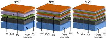
In the present work, we have attempted to overcome the metal inter-diffusion problem using multi-stacked layers of metal precursors. We have prepared CZTS films on Mo-coated glass substrates using 3-layer metallic precursors in the sequence Sn/ZnS/Cu (3LYS). Additionally, using a repeating sequence of Sn/ZnS/Cu on glass substrates covered with Mo, we created 6-layer and 9-layer metallic precursors, referred to as 6-LYS and 9LYS, respectively. The structural properties, morphological changes, optical properties, impurity phase formation, and photoresponse of 3LYS, 6LYS, and 9LYS samples are compared. We found that the photoresponse can be improved from ∼19 μA cm−2 (via 3LYS) to ∼38 μA cm−2 (via 6LYS) to ∼82 μA cm−2 (via 9LYS) due to compact uniform microstructure and enhanced crystal quality along with suppression of secondary phase formation in 9LYS sample.
2 Experimental
2.1. Preparation of CZTS stacking layers
The CZTS thin films were prepared on Mo-coated glass substrates, followed by the sulfurization of deposited metallic precursors. The new procedure resulted in the precursor being progressively deposited from Cu (99.99%), ZnS (99.99%), and Sn (99.99%) targets at room temperature via RF sputtering, as shown in Fig. 1.The stacking of the precursor's overall thickness was kept constant at 700 nm. We used 2 cm2 Mo-coated corning glass substrates prepared by our own calibrated DC sputtering method40 having a thickness of ∼1 μm and sheet resistance of 2 Ω per □. The Mo-coated glass substrates were cleaned using an ultrasonic cleaner for ten minutes each in acetone and deionized water. Then, they were blow-dried in N2 (99.99%) gas to prepare the substrates for sputtering. Working gas pressure was maintained at 1.5 Pa (base pressure below 5 × 10⁻⁴ Pa), and precursors were kept in an atmosphere of Ar (99.99%). ZnS was deposited via sputtering power maintained at 120 W, and Cu and Sn required 70 W. Thickness of each precursor layer was controlled using deposition time. For example, the 3LYS metallic precursor was layered in the following order: Sn/ZnS/Cu, which were then repeated twice for 6LYS and three times for 9LYS, all resulting in a thickness of ∼700 nm. In the sulfurization process, all the multi-stacked precursor films are kept in a tubular furnace in an Ar atmosphere at ambient pressure. After that, heating was started, and at a temperature of 550 °C, 5% H2S gas was mixed with Ar for the next 10 min. After 10 min, the H2S supply was cut, and samples were rapidly cooled to room temperature in an Ar atmosphere.
2.2. Characterization of CZTS stacking layers
Various complementary characterization techniques have been used to analyze CZTS thin films. An X-ray diffractometer (XRD) (Bruker D8 Advance, Germany) was used to analyze the CZTS thin films using the Cu-K line (=1.54) at a 1° grazing angle. The He–Ne (532 nm) laser was used to capture the Raman spectra by keeping laser power below 10 mW to prevent laser-induced crystallization. A JASCO UV-670 UV-visible spectrometer measured the optical absorption spectra between 400 and 1200 nm. An FEI, Nova NanoSem 450 scanning electron microscope was used to obtain field emission scanning electron micrographs (FE-SEM) of CZTS thin films. Thermo Scientific's K-Alpha+, UK machine with a resolution of 0.1 eV, was used to conduct X-ray photoelectron spectroscopy (XPS). Utilizing Al–K (1486.6 eV) radiation, we have captured XPS spectra for the particular element. After several scans in the acquisition process, the XPS signals were captured. By referring to C 1s at 284.6 eV, the binding energy was adjusted for specimen charging. A Metrohm Autolab: PGSTAT302N potentiostat and a Xenon lamp of 150 W (PEC-L01) assessed thin films' photocurrent density–time (J–t) characteristics.3 Results and discussion
3.1. X-ray diffraction (XRD) analysis
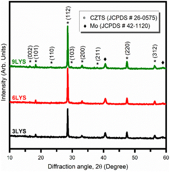
As evident from Table 1, the different matrix has different diffusion lengths, and as expected, the 9LYS sample exhibited better inter-diffusion, resulting in homogenous composition and improved CZTS crystal quality. Therefore, XRD was used to confirm the phase formation and crystallinity of tetragonal kesterite-CZTS films. The diffractogram of these three sulfurized CZTS samples is shown in Fig. 2.It should be noted that the Zn to Cu matrix and the Sn to Zn matrix have shorter diffusion lengths than other matrices at a sulfurization temperature of 550 °C, as indicated in Table 1.
As evident from Table 1, the different matrix has different diffusion lengths, and as expected, the 9LYS sample exhibited better inter-diffusion, resulting in homogenous composition in the resultant CZTS films. Therefore, X-RD was used to confirm the phase formation and crystallinity of tetragonal kesterite-CZTS films. The diffractogram of these three sulfurized CZTS samples is shown in Fig. 2.
The prominent peak (112) of CZTS has different intensities, although there are no appreciable differences in the XRD peak positions. With more stacking layers, the (112) peak becomes more intense. Therefore, the 3LYS sample has weaker intensity compared to 6LYS and 9LYS samples. The overall volume of CZTS in a film can explain this decreased diffraction intensity. It should be noted that the Zn to Cu matrix and the Sn to Zn matrix have diffusion lengths of around 150 nm and 290 nm, respectively, at a sulfurization temperature of 550 °C (See Table 1). With these finite diffusion lengths, we anticipate superior inter-diffusion in the 9LYS precursor during the sulfurization process, resulting in a homogeneous composition and distribution in the resulting CZTS film. The prominent peaks are shown at 28.53°, 47.47°, and 56.29° correlate to the CZTS (112), (220), and (312) planes and are indicative of the kesterite structure (tetragonal system) [JCPDS card # 26-0575]. Some structural parameters like crystallite size (D), texture coefficient (TC), dislocation density (δ), average micro-strain (ε), etc., are extracted from the XRD pattern.
Scherrer's formula is used to determine the average crystallite size,41
 | (1) |
The degree of preferred orientation of the different crystalline planes can be determined from Harris's analysis42 by calculating the texture coefficient (TC) using,
 | (2) |
The calculated values of the texture coefficient for stacking layers 3LYS, 6LYS, and 9LYS are listed in Table 2.
| Sample | TC (112) | D (nm) | δ × 10−4 nm−2 | ε × 10−3 |
|---|---|---|---|---|
| 3LYS | 1.68 | 48 | 4.3 | 2.9 |
| 6LYS | 1.73 | 41 | 5.9 | 3.4 |
| 9LYS | 1.88 | 41 | 5.9 | 3.4 |
A crystallographic flaw or irregularity called a dislocation, which exists within a crystal structure, significantly impacts material properties. According to eqn (3), the dislocation density (δ) is the length of dislocation lines per unit volume of the crystal,43
 | (3) |
The displacement of the unit cell from its usual position causes the lattice micro-strain (ε) in a crystal. Lattice misfits, including flaws like dislocation, stacking fault likelihood, and lattice distortion, cause them to appear in CZTS thin films. Microstrain is calculated via the following equation,
 | (4) |
The values of micro-strain for stacking layers 3LYS, 6LYS, and 9LYS are listed in Table 2. For the 9LYS CZTS film, the texture coefficient shows a much larger deviation from unity, which implies that the preferred orientation growth of the (112) plane is significantly higher than the 3LYS CZTS film. In addition, 9LYS CZTS film has a comparatively smaller crystallite size than 3LYS. However, it has a much higher crystallite volume fraction, which will help increase the charge carrier mobility.
3.2. Raman spectroscopy analysis
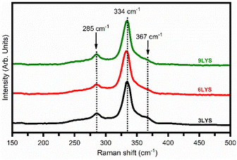
CZTS has a crystal structure identical to that of ZnS and Cu2SnS3, so it isn't easy to discern between the peaks of secondary phases (specifically ZnS, Cu2SnS3, and Cu3SnS4) and that of CZTS. Thus, fabricated films were investigated via. Raman spectroscopy is used to validate the presence of secondary phases, i. e. ZnS and Cu2SnS3. Fig. 3 shows Raman spectra for multi-stacked layer precursor 3LYS, 6LYS, and 9LYS CZTS thin films. The Raman spectra show a strong band at ∼334 cm−1, which agrees with the earlier reports on CZTS films.21,44 There were no additional peaks in the Raman spectra that corresponded to ZnS (350 cm−1), Cu2−xS (471–473 cm−1), and Cu2SnS3 (298 cm−1),45–47 indicating that the pure phase of kesterite-CZTS had formed. Chen et al.38 studied depth-resolved Raman spectroscopy of multi-stacked CZTS films. They also observed lower impurity levels and better metal inter-diffusion in the 9-layer stacking of precursor.3.3. X-ray photoelectron spectroscopy analysis
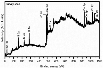
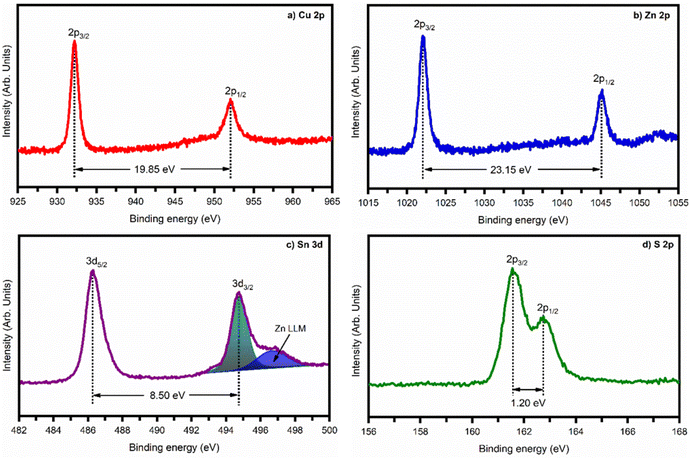
Fig. 4 shows a typical survey spectrum of 9LYS CZTS thin film, which indicates that the presence of copper (Cu), zinc (Zn), tin (Sn), sulfur (S), and carbon (C) from reference and oxygen (O) from impurity. In Fig. 5(a) 9LYS sample shows pronounced splitting of the Cu 2p spectral line into the 2p1/2 and 2p3/2 core levels peaks at ∼952.05 eV and ∼ 932.2 eV with spectral line splitting of 19.85 eV that allows concluding that copper is in the +1 oxidation state indicating the formation of Cu(I).22,48 Fig. 5(b) 9LYS sample shows Zn 2p core level spectra which exhibit Zn 2p3/2 and 2p1/2 peaks visible at a binding energy of ∼ 1045.2 and ∼ 1022.05 eV with a spectral line separation of 23.15 eV suggesting the presence of zinc(II).22,48 The separation between Sn 3d5/2 and Sn 3d3/2 was 8.5 eV, shown in Fig. 5(c), indicating the presence of tin in the Sn(IV) state.22,48,49 The peak splitting between S 3p3/2 and 3p1/2 is 1.22 eV, which is in accordance with the expected S value (160–164 eV) in the sulfide phases.3.4. Field-emission scanning electron microscopy analysis
Fig. 6 shows the surface morphology of sputter-grown 3LYS, 6LYS, and 9LYS multi-stacked layers of CZTS films. The 9-layer stacking precursor film showed well-defined CZTS grain and became well-faceted with densely packed granular film morphology [Fig. 6(c)]. Round particles packed on the surface were seen in the 3LYS precursor, and the 6LYS precursor showed rough morphology with discernible micro-voids [Fig. 6(c)], resulting in a poor interface.36 The 9LYS precursor, meanwhile, yielded a thin, flat sheet that was relatively compact. Large agglomerated micrograins are observed in the 9LYS sample, which is advantageous from the perspective of solar cell applications since it lessens the recombination of photogenerated charge carriers. The average grain size of CZTS was calculated using the ImageJ application and significantly improved in the 9LYS precursor, which is ∼0.7–0.8 μm than the conventional 3LYS sample.The non-stoichiometry of compound semiconductors always correlates with their physicochemical properties. For example, for high-performing CZTS solar cell absorbers, there is an empirical rule that the Cu/(Zn + Sn) and Zn/Sn atomic ratios should lie in the range of 0.75–1.0 and 1.0–1.25, respectively.50 The compositional data obtained from energy-dispersive X-ray analysis (EDAX) are shown in Table 3. The EDAX shows elemental composition is near the stoichiometric ratio. But the increase in compositional ratios of Cu/(Zn + Sn) and (Zn/Sn) indicates the loss of Sn during sulfurization.
| Sample | Elemental composition (atomic %) | Composition ratio | |||||
|---|---|---|---|---|---|---|---|
| Cu | Zn | Sn | S | Cu/(Zn + Sn) | Zn/Sn | S/(Cu + Zn + Sn) | |
| 3LYS | 21.12 | 12.61 | 11.14 | 55.13 | 0.88 | 1.13 | 1.22 |
| 6LYS | 23.37 | 14.27 | 12.35 | 50.01 | 0.87 | 1.15 | 1.01 |
| 9LYS | 24.03 | 15.09 | 11.43 | 49.45 | 0.90 | 1.32 | 0.98 |
3.5. UV-vis spectroscopy analysis
The optical properties of CZTS films (optical absorption and bandgap) were studied using UV-visible spectroscopy. The absorbance plot of multi-stacked CZTS samples in Fig. 7(a) indicates that all precursors show high optical absorbance in the visible region. However, the 9LYS precursor shows significantly enhanced absorption in the visible region due to its high crystalline volume fraction and well-defined grain morphology. According to Tauc et al.,51 the optical band gap (Eg) calculations were carried out. The region of the solar spectrum that a CZTS absorber will absorb depends on the optical band gap. By extrapolating the linear portion of the (αhν)2 vs. hν plot shown in Fig. 7(b), it is possible to determine the band gap energy (Eg) for direct transitions. The band gap energies of all CZTS samples are observed in the range between 1.47 eV and 1.51 eV. Band gap variation is mainly attributed to variations in the homogeneity and crystallinity of the films, which in turn cause variations in the size of the crystallites between the samples.52 Therefore, the band gap values are relatively near the ideal band gap for solar cells.53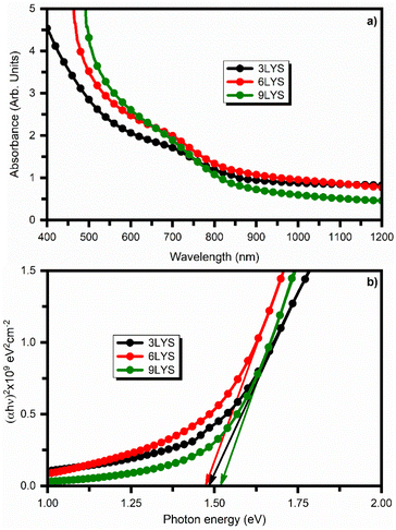 | ||
| Fig. 7 (a) Absorption spectra of multi-stacked precursor CZTS thin films and (b) Tauc plot used to estimate optical energy band gap. | ||
3.6. Photoresponse and impedance measurements
Measurements of photoresponse and impedance were performed using a standard three-electrode system. For the measurements, a buffer layer of cadmium sulfide (CdS) was coated onto the multi-stacked CZTS thin films by sputtering. To maintain the spectral response of the multi-stacked precursors CZTS films, the thickness of the CdS layer was kept between 50–60 nm. The schematic of prepared CZTS(3LYS/6LYS/9LYS)/CdS films for photoresponse and impedance measurement is shown in Fig. 8(a). Saturated calomel electrodes (SCE), platinum mesh, and CZTS(3LYS/6LYS/9LYS)/CdS on Mo-coated glass substrate were utilized as the working electrode, counter electrode and reference electrode, respectively. The schematic of the conventional three-electrode cell is shown in Fig. 8(b). Additionally, a 5 mM redox electrolyte of europium nitrate hydrate [Eu(III)(NO3)3·6H2O] was employed as an electron scavenger.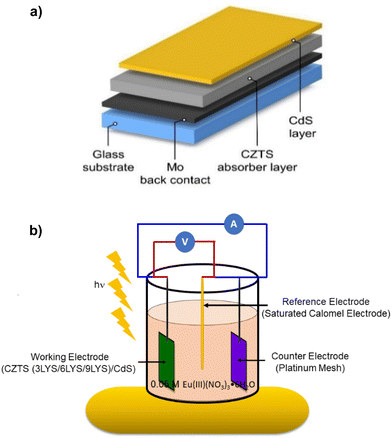 | ||
| Fig. 8 Schematic of (a) CZTS/CdS junction (b) conventional three-electrode cell employed in the present study. | ||
The impedance measurement is susceptible to light illumination. In impedance spectra, the arc radius describes the junction resistance between the semiconductor surface and the electrolyte. An equivalent electrical circuit replicates and fits impedance spectroscopy data from the Nyquist plot. The inset of Fig. 9 displays the electrical parts used in the corresponding circuit.
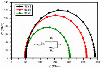 | ||
| Fig. 9 Impedance spectra of synthesized CZTS thin films using multi-stacked layer precursors. The inset contains the equivalent circuit diagram. | ||
After fitting electrochemical impedance spectroscopy (EIS) data with the equivalent circuit, 9LYS thin film showed the lowest charge transfer resistance (Rct = 154.14 Ω) compared to the conventional 3LYS thin film (Rct = 240.08 Ω), which suggested that it can help to improved electrical conductivity. It could be responsible for achieving high photocurrent in solar cell applications. The photoresponse of fabricated CZTS films, as quantified by the transient photocurrent density (J–t) upon the light irradiation (1000 W m−2) in AM 1.5, is shown in Fig. 10.
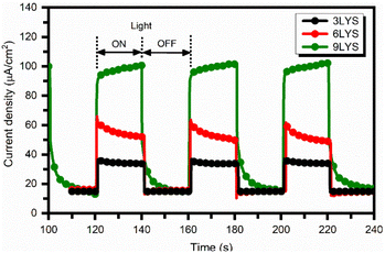 | ||
| Fig. 10 Transient photocurrent density as a function of time for multi-stacked precursors CZTS films biased at −0.5 V. | ||
When the light is turned ON and OFF under chopping conditions, a rapid rise and fall of photocurrent are observed. When the electrode is illuminated, the photogenerated holes migrate to the back electrode (Mo), and the photogenerated electrons migrate into the electrolyte, resulting in a dramatic increase in photocurrent. In addition, for measurements, the active area of each sample was kept constant at 10 mm × 10 mm, which is determined by the masked residual area. Interestingly, the photocurrent density in 9LYS CZTS was about twice that of 6LYS and four times larger than of conventional 3LYS CZTS film for a given bias voltage of −0.5 V because of higher light absorption, reduced electron–hole recombination, and increased charge transfer at the interface. Our prepared multi-stacked precursors 9LYS CZTS film shows a maximum photocurrent density of 82 μA cm−2 is much superior to the other CZTS reported in the literature.13,54–57 These findings suggest that the multi-stacked-layer modification dramatically impacts the performance of the CZTS absorber from 3LYS to 9LYS.
Fig. 10 shows the dark current (Id) corresponding to all prepared CZTS films (for 3LYS Id = 14.7 μA, for 6LYS Id = 16.1 μA and for 9LYS Id = 15.2 μA) are nearby same but on the higher side as compared to work done previously.23,33,57,58 Therefore, one can further work on suppressing the dark current along with the increase in the photocurrent, which is a prerequisite for photoresponse enhancement, which allows multi-stacked precursors CZTS films to perform even better. Courel et al.59 carried out a detailed analysis of different loss mechanisms and their contribution to the dark current density to understand what limits the performance of the CZTS-based solar cells.
Fig. 11 shows rise and decay curves (exponential fitted) of multi-stacked precursors CZTS films in the presence of 1000 W m−2 light irradiation in AM 1.5 at a bias of −0.5 V. The fitted curves confirm the exponential time dependency. The estimated rise time (decay time) for 3LYS and 6LYS is 28 ms (120 ms) and 15 ms (92 ms), respectively. The rise and decay time obtained for 6LYS is significantly low compared to the reported literature.13,33 Though we observed high rise time (294 ms) and decay time (1980 ms) for the 9LYS sample as compared to 3LYS and 6LYS, the sensitivity, responsivity, and detectivity of the 9LYS sample shown in Table 3 are significantly enhanced due to superior inter-diffusion of metallic precursors improved crystal quality of CZTS.
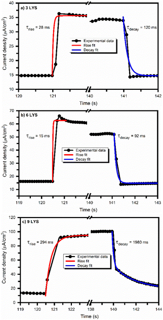 | ||
| Fig. 11 Exponential fitted rise and decay photoconductivity curve of multi-stacked precursors CZTS films. | ||
Sensitivity (S) is defined as the relative increase in the current when a light source illuminates the film and is measured using relation,60
 | (5) |
Responsivity (R) is the amount of photocurrent generated when a light source illuminates the films and is evaluated by the formula,61
 | (6) |
The detectivity of prepared CZTS thin films was calculated by the relation,62
 | (7) |
The sensitivity (S), responsivity (R), and detectivity (D) of all photodetectors are tabulated in Table 4.
| Sample | ID (μA) | IL (μA) | Iph (μA) | S (%) | R (mA W−1) | D × 109 (Jones) |
|---|---|---|---|---|---|---|
| 3LYS | 14.7 | 34.1 | 19.4 | 131 | 0.194 | 0.89 |
| 6LYS | 16.1 | 54.2 | 38.1 | 237 | 0.381 | 1.68 |
| 9LYS | 15.2 | 97.1 | 81.9 | 539 | 0.819 | 3.71 |
The responsivity of CZTS films increases from 0.194 to 0.819 mA W−1 with an increase of multi-stacked precursor from 3 layers to 9 layers, which may be due to the decrease in resistivity and increase of mobility of the films. It is, therefore, possible to forecast that thicker metallic precursor stacks with higher metallic precursor numbers, like 12 LYS, may be feasible. However, based on this study, the 9 LYS should be close to the restricted values due to two critical factors diffusion length and thickness of the individual layer. At the same time, a device with poor performance will arise from the precursor's (mostly sulfur's) interaction with the Mo substrate at greater sulfurization temperatures and over a more extended period. Multi-stacked 9-layer with sulfurization at 550 °C for 10 min is the best approach to improve device performance.
4 Conclusion
In conclusion, we showed that three types of high-quality CZTS thin films might be produced by sulfurizing a multi-stacking Sn/ZnS/Cu metallic precursor via RF-magnetron sputtering in an environment of H2S and argon (kept at room temperature and ambient pressure). On an increasing number of stacked layers, i. e. from 3LYS to 9LYS system, there is an enhancement in the crystal quality, surface morphology, and photoresponse of CZTS films. Furthermore, in the case of the 9LYS sample, the improved inter-diffusion within stacked metallic layers resulted in a significant enhancement in crystallinity and homogenous grain size distribution throughout the film. Finally, in this work, CZTS thin film is fabricated via a modified stacked metallic precursor sequence exhibited a larger photocurrent density in the 9LYS (∼82 μA cm−2) sample as compared to 6LYS (∼38 μA cm−2) and 3LYS (∼19 μA cm−2) samples. These results demonstrate that optimizing stacked metallic precursor sequences while fabricating CZTS thin films can play a vital role in improving the overall performance of the realized films for solar cell applications.Author contribution
Subhash Pandharkar: methodology, formal analysis, investigation, data curation, writing-original draft. Yogesh Hase: methodology, conceptualization, validation, formal analysis, investigation. Shruti Shah: methodology, validation, formal analysis, investigation. Vidya Doiphode: methodology, validation, formal analysis, investigation. Ashish Waghmare: methodology, conceptualization, validation, investigation. Ashvini Punde: methodology, validation, formal analysis, investigation. Pratibha Shinde: conceptualization, validation, formal analysis, investigation. Swati Rahane: data curation, formal analysis, investigation. Bharat Bade: conceptualization, validation, formal analysis, investigation. Somnath Ladhane: data curation, formal analysis, investigation. Mohit Prasad: data curation, writing-review, and editing. Shashikant P. Patole: writing-review and editing. Sandesh Jadkar: visualization, writing-review, editing, supervision, funding acquisition.Conflicts of interest
There are no conflicts to declare.Acknowledgements
Subhash Pandharkar, Yogesh Hase, Shruti Shah, Vidya Doiphode, Ashish Waghmare, Pratibha Shinde, and Bharat Bade are thankful to the Ministry of New and Renewable Energy (MNRE), Government of India, for the financial support under the National Renewable Energy Fellowship (NREF) program. Ashvini Punde is thankful to the Mahatma Jyotiba Phule Research and Training Institute (MAHAJYOTI), Government of Maharashtra, for the Mahatma Jyotiba Phule Research Fellowship (MJPRF). Swati Rahane is thankful for the research fellowship to the Chhatrapati Shahu Maharaj Research, Training and Human Development Institute (SARTHI), Government of Maharashtra. Finally, Mohit Prasad and Sandesh Jadkar are grateful to the Indo-French Centre for the Promotion of Advanced Research-CEFIPRA, Department of Science and Technology, New Delhi, for special financial support. Shashikant P. Patole would like to thank Khalifa University for its financial support through the internal fund for high-quality publications.References
- K. S. Gour, V. Karade, P. Babar, J. Park, D. M. Lee, V. N. Singh and J. H. Kim, Sol. RRL, 2021, 5, 2000815 CrossRef CAS.
- M. P. Suryawanshi, U. V. Ghorpade, C. Y. Toe, U. P. Suryawanshi, M. He, D. Zhang, J. S. Jang, S. W. Shin, J. H. Kim, X. Hao and R. Amal, Prog. Mater. Sci., 2023, 134, 101073 CrossRef CAS.
- F. Liu, Q. Zeng, J. Li, X. Hao, A. Ho-Baillie, J. Tang and M. A. Green, Mater. Today, 2020, 41, 120 CrossRef CAS.
- H. Katagiri, K. Jimbo, W. S. Maw, K. Oishi, M. Yamazaki, H. Araki and A. Takeuchi, Thin Solid Films, 2009, 517, 2455 CrossRef CAS.
- S. Ge, H. Xu, Y. Huang, S. K. Karunakaran, R. Hong, J. Li, Y. Mai, E. Gu, X. Lin and G. Yang, Sol. RRL, 2020, 4, 2000325 CrossRef CAS.
- J. Jianga, L. Zhangb, W. Wanga and R. Hong, Ceram. Int., 2018, 44, 11597 CrossRef.
- L. Sun, J. He, H. Kong, F. Yue, P. Yang and J. Chu, Sol. Energy Mater. Sol. Cells, 2011, 95, 2907 CrossRef CAS.
- S. Giraldo, Z. Jehl, M. Placidi, V. Izquierdo-Roca, A. Pérez-Rodríguez and E. Saucedo, Adv. Mater., 2019, 31, 1806692 CrossRef PubMed.
- H. Katagiri, Thin Solid Films, 2005, 480–481, 426 CrossRef CAS.
- C. Zeng, Y. Liang, L. Zeng, L. Zhang, J. Zhou, P. Huang and R. Hong, Sol. Energy Mater. Sol. Cells, 2019, 203, 110167 CrossRef CAS.
- Y. Liang, C. Zeng, L. Zeng, G. Yan, Y. Yuan, X. Lin, H. Zhu, Y. Mai and R. Hong, Sol. RRL, 2022, 6, 2101047 CrossRef CAS.
- S. Ge, H. Xu, S. N. Khan, W. Yang, R. Hong, Y. Mai, E. Gu, X. Lin and G. Yang, Sol. RRL, 2021, 5, 2100598 CrossRef CAS.
- O. P. Singh, A. Sharma, K. S. Gour, S. Husale and V. N. Singh, Sol. Energy Mater. Sol. Cells, 2016, 157, 28 CrossRef CAS.
- F. Jiang, S. Ikeda, T. Harada and M. Matsumura, Adv. Energy Mater., 2014, 4, 1301381 CrossRef.
- Q. Guo, G. M. Ford, W. C. Yang, B. C. Walker, E. A. Stach, H. W. Hillhouse and R. Agrawal, J. Am. Chem. Soc., 2010, 132, 17384 CrossRef CAS PubMed.
- W. Wang, M. T. Winkler, O. Gunawan, T. Gokmen, T. K. Todorov, Y. Zhu and D. B. Mitzi, Adv. Energy Mater., 2014, 4, 1301465 CrossRef.
- S. W. Shin, S. M. Pawar, C. Y. Park, J. H. Yun, J. H. Moon, J. H. Kim and J. Y. Lee, Sol. Energy Mater. Sol. Cells, 2011, 95, 3202 CrossRef CAS.
- G. Zoppi, I. Forbes, R. W. Miles, P. J. Dale, J. J. Scragg and L. M. Peter, Prog. Photovolt.: Res. Appl., 2009, 17, 315 CrossRef CAS.
- C. Shi, G. Shi, Z. Chen, P. Yang and M. Yao, Mater. Lett., 2012, 73, 89 CrossRef CAS.
- V. Tunuguntla, W. C. Chen, P. H. Shih, I. Shown, Y. R. Lin, J. S. Hwang, C. H. Lee, L. C. Chen and K. H. Chen, J. Mater. Chem. A, 2015, 3, 15324 RSC.
- B. R. Bade, S. R. Rondiya, Y. A. Jadhav, M. M. Kamble, S. V. Barma, S. B. Jathar, M. P. Nasane, S. R. Jadkar, A. M. Funde and N. Y. Dzade, J. Alloys Compd., 2021, 854, 157093 CrossRef CAS.
- S. C. Riha, B. A. Parkinson and A. L. Prieto, J. Am. Chem. Soc., 2009, 131, 12054 CrossRef CAS PubMed.
- L. S. Khanzada, M. A. Makhdoom, X. Lin, H. Azimi and C. J. Brabec, Optik, 2023, 272, 170381 CrossRef CAS.
- M. A. Makhdoom, V. Sgobba, L. S. Khanzada, S. Fladischer and E. Spiecker, Phys. Status Solidi A, 2019, 2016, 1900040 CrossRef.
- S. Chen, A. Walsh, X. Gong and S. Wei, Adv. Mater., 2013, 25, 1522 CrossRef CAS PubMed.
- D. H. Son, D. H. Kim, S. N. Park, K. J. Yang, D. Nam, H. Cheong and J. K. Kang, Chem. Mater., 2015, 27, 5180 CrossRef CAS.
- J. J. Scragg, T. Ericson, X. Fontané, V. Izquierdo-Roca, A. Pérez-Rodríguez, T. Kubart, M. Edoff and C. Platzer-Björkman, Prog. Photovolt.: Res. Appl., 2014, 22, 10 CrossRef CAS.
- I. V. Dudchak and L. V. Piskach, J. Alloys Compd., 2003, 351, 145 CrossRef CAS.
- S. Kim, J. A. Marquez, T. Unold and A. Walsh, Energy Environ. Sci., 2020, 13, 1481 RSC.
- T. K. Todorov, J. Tang, S. Bag, O. Gunawan, T. Gokmen, Y. Zhu and D. B. Mitzi, Adv. Energy Mater., 2013, 3, 34 CrossRef CAS.
- D. Shin, B. Saparov and D. B. Mitzi, Adv. Energy Mater., 2017, 7, 1602366 CrossRef.
- G. Yan, C. Zeng, Y. Yuan, G. Wang, G. Cen, L. Zeng, L. Zhang, Y. Fu, C. Zhao, R. Hong and W. Mai, ACS Appl. Mater. Interfaces, 2019, 11, 32097 CrossRef CAS PubMed.
- K. S. Gour, B. Bhattacharyya, O. P. Singh, A. K. Yadav, S. Husale and V. N. Singh, J. Alloys Compd., 2018, 735, 285 CrossRef CAS.
- Y. Xie, C. Zhang, F. Yue, Y. Zhang, Y. Shic and T. Ma, RSC Adv., 2013, 3, 23264 RSC.
- C. Zha, C. Ji, J. Zhang, L. Shen, X. Zhang, S. Dongb and N. Bao, RSC Adv., 2016, 6, 107151 RSC.
- A. Fairbrother, L. Fourdrinier, X. Fontané, V. Izquierdo-Roca, M. Dimitrievska, A. Pérez-Rodríguez and E. Saucedo, J. Phys. Chem. C, 2014, 118, 17291 CrossRef CAS.
- R. B. V. Chalapathy, G. S. Jung and B. T. Ahn, Sol. Energy Mater. Sol. Cells, 2011, 95, 3216 CrossRef CAS.
- W. C. Chen, C. Y. Chen, V. Tunuguntla, S. H. Lu, C. Su, C. H. Lee, K. H. Chen and L. C. Chen, Nano Energy, 2016, 30, 762 CrossRef CAS.
- E. A. Brandes, E. A. Brooks and G. B. Smithells, Metal Reference Book, Oxford, 1992 Search PubMed.
- S. M. Pandharkar, S. R. Rondiya, A. V. Rokade, B. B. Gabhale, H. M. Pathan and S. R. Jadkar, Front. Mater., 2018, 5, 13 CrossRef.
- B. D. Cullity and S. R. Stock, Elements of X-Ray Diffraction, Princeton Hall, 2001 Search PubMed.
- G. B. Harris, London, Edinburgh Dublin Philos. Mag. J. Sci., 1952, 43, 113 CrossRef.
- V. T. Tiong, T. Hreid, G. Will, J. Bell and H. Wang, Sci. Adv. Mater., 2014, 6, 1467 CrossRef CAS.
- P. Prabeesh, I. P. Selvam and S. N. Potty, Appl. Phys. A, 2018, 124, 225 CrossRef.
- A. Fairbrother, X. Fontané, V. Izquierdo-Roca, M. Espíndola-Rodríguez, S. López-Marino, M. Placidi, L. Calvo-Barrio, A. Pérez-Rodríguez and E. Saucedo, Sol. Energy Mater. Sol. Cells, 2013, 112, 97 CrossRef CAS.
- A. J. Cheng, M. Manno, A. Khare, C. Leighton, S. A. Campbell and E. S. Aydil, J. Vac. Sci. Technol., A, 2011, 29, 051203 CrossRef.
- G. Y. Kim, J. R. Kim, W. Jo, K. D. Lee, J. Y. Kim, T. T. T. Nguyen and S. Yoon, Curr. Appl. Phys., 2014, 14, 1665 CrossRef.
- J. Xu, X. Yang, Q. D. Yang, T. L. Wong and C. S. Lee, J. Phys. Chem. C, 2012, 116, 19718 CrossRef CAS.
- N. J. Choudhari, Y. Raviprakash, B. J. Fernandes and N. K. Udayashankar, J. Alloys Compd., 2019, 799, 314 CrossRef CAS.
- H. Chen, Q. Ye, X. He, J. Ding, Y. Zhang, J. Han, J. Liu, C. Liao, J. Meia and W. Lau, Green Chem., 2014, 16, 3841 RSC.
- J. Tauc and A. Menth, J. Non. Cryst. Solids, 1972, 8–10, 569–585 CrossRef CAS.
- M. C. Rao and S. S. Basha, Results Phys., 2018, 9, 996 CrossRef.
- S. M. Pawar, B. S. Pawar, A. V. Moholkar, D. S. Choi, J. H. Yun, J. H. Moon, S. S. Kolekar and J. H. Kim, Electrochim. Acta, 2010, 55, 4057 CrossRef CAS.
- R. Mudike, A. Bheemaraju, T. Rasheed, N. Singh, S. R. Dhage, P. D. Shivaramu and D. Rangappa, Ceram. Int., 2022, 48, 35666 CrossRef CAS.
- V. Mahalakshmi, D. Venugopal, K. Ramachandran and R. Ramesh, J. Mater. Sci.: Mater. Electron., 2022, 33, 8493 CrossRef CAS.
- Nisika, K. Kaur, K. Arora, A. H. Chowdhury, B. Bahrami, Q. Qiao and M. Kumar, J. Appl. Phys., 2019, 126, 193104 CrossRef.
- Z. Hou, Y. Li, J. Liu, H. Shena and X. Huo, New J. Chem., 2021, 45, 1743 RSC.
- Y. F. Tay, S. S. Hadke, M. Zhang, N. Lim, S. Y. Chiamd and L. H. Wong, J. Mater. Chem. A, 2020, 8, 8862 RSC.
- M. Courel, J. A. Andrade-Arvizu and O. Vigil-Galán, Solid-State Electron., 2015, 111, 243 CrossRef CAS.
- M. S. Mahdi, K. Ibrahim, N. M. Ahmed, A. Hmood, F. I. Mustafa, S. A. Azzez and M. Bououdina, J. Alloys Compd., 2018, 735, 2256 CrossRef CAS.
- A. Sharma, B. Bhattacharyya, A. K. Srivastava, T. D. Senguttuvan and S. Husale, Sci. Rep., 2016, 6, 19138 CrossRef CAS PubMed.
- D.-H. Kwak, D.-H. Lim, H.-S. Ra, P. Ramasamya and J.-S. Lee, RSC Adv., 2016, 6, 65252 RSC.
| This journal is © The Royal Society of Chemistry 2023 |

