
 Open Access Article
 This Open Access Article is licensed under a Creative Commons Attribution-Non Commercial 3.0 Unported Licence
Reduced electron relaxation time of perovskite films via g-C3N4 quantum dot doping for high-performance perovskite solar cells†
Lu-Lu Jiang *,
Meng-Meng Chen,
Xiao-Dan Tang,
Ying Tang,
Shao-Jie Li,
Ying Li,
Hang-Hui Li and
Hai-Rui Liu*
*,
Meng-Meng Chen,
Xiao-Dan Tang,
Ying Tang,
Shao-Jie Li,
Ying Li,
Hang-Hui Li and
Hai-Rui Liu*
College of Material Science and Engineering, Henan Normal University, Xinxiang 453000, China
First published on 6th June 2023
Abstract
Perovskite film-quality is a crucial factor to improve the photovoltaic properties of perovskite solar cells, which is closely related to the morphology of crystallization grain size of the perovskite layer. However, defects and trap sites are inevitably generated on the surface and at the grain boundaries of the perovskite layer. Here, we report a convenient method for preparing dense and uniform perovskite films, employing g-C3N4 quantum dots doped into the perovskite layer by regulating proper proportions. This process produces perovskite films with dense microstructures and flat surfaces. As a result, the higher fill factor (0.78) and a power conversion efficiency of 20.02% are obtained by the defect passivation of g-C3N4QDs.
Introduction
Organic–inorganic hybrid perovskite solar cells (PSCs) have attracted intensive attention in the last few years due to outstanding photoelectric properties of perovskite semiconductor materials such as longer exciton diffusion length, higher absorption coefficient and easier tunable direct bandgap,1–3 which have promoted high power conversion efficiencies (PCEs) of PSCs to the current world record of 25.7% (ref. 4) based on a single junction device. Particularly, the perovskite light-absorbing layer attracts much attention by its simple and low-temperature fabrication technology.5–8 The crystal quality, surface morphology and grain size9,10 of a perovskite active layer is the key point for high-performance PSCs.11–13 There are many ways to optimize the crystalline process of a perovskite layer such as solution engineering,14 ion doping15 etc., which controls the crystallization of perovskite film by modifying nucleation and growing-process are important measures toward achieving high quality perovskite films.16,17 Nevertheless, the relationship between perovskite crystal dynamics and film properties has not been thoroughly studied so far, especially the relationship between the electronic relaxation time of perovskite layer and device properties is also rarely studied.As the light-absorbing layer of PSCs, perovskite layer plays a significantly important role in the performance of devices. Several works have been published to highlight the contribution of central structure to the performance of PSCs. It is very effective to optimize central structure of devices by using doped semiconductor and nanometer material into the perovskite layer and transport layer.18–20 As examples, Liao group21 achieved a PCE of 19.49% by doping a 2D polymeric material of graphitic carbon nitride (g-C3N4) into the perovskite layer to reduce its intrinsic defect density. Wu et al.22 utilized the synergistic effect of H2O and DMF preparing a high-quality and large-area perovskite film, which realized a high PCE of 20.1%. Chen et al.23 demonstrated the planar heterojunction solar cells with a PCE of 18.4% improved from 16.0% by presenting the Ag incorporated organic-inorganic perovskite films. Nucleation and crystal growth are the key factors in the controllable morphology of solution processed perovskite film.24–26 In general, the growth of perovskite layer is dependent on precursor composition, solvent choice, deposition temperature and time, and so on, which is regarded as the fascinating role to improve the optoelectronic properties of PSCs.27,28 Especially, solvent engineering plays very effective role in the controllable growth of solution-processed crystalline films. Moreover, due to the perovskite crystalline nature, the perovskite interfaces also influence the device performance.29 In addition, less grain boundaries and thickness of perovskite layer are all also key elements contribute to high-efficiency PSCs.30–34 Large grains can improve the perovskite film morphology and coverage effectively to reach an enhanced light-harvesting under unified light intensity.35–39
The studies of quantum dots modified PSCs mainly focused on the application of carbon quantum dots (CQDs) in devices, and the application of g-C3N4QDs in PSCs is rarely reported. Huang group40 have introduced CQDs with hydroxyl and carbonyl groups on the surface into perovskite precursor solutions, where the functional groups interact with lead ions to form an intermediate phase, effectively reducing non-radiative recombination and preparing efficient and stable solar cells. Compared to CQDs, g-CNQDs have abundant functional groups on their surface, which promotes the forming of intermediate phases in perovskite precursor solutions. By adjusting the concentration, the nucleation sites during the perovskite crystallization process can be controlled, thereby optimizing the quality of perovskite thin films.
The graphene-like material was synthesized by hydrothermal method, and then its quantum dots were prepared by ultrasonic stripping. Herein, we fabricate the high-performance PSCs based on perovskite light-absorbing layer doped with Quantum Dots (QDs). The suitable doping of QDs increases perovskite crystallization grain size by hydroxylamine and carboxyl groups, which reduces intrinsic defect density by passivating the charge recombination centers around the grain boundaries. Moreover, the electronic relaxation time is reduced and the current density of the device is effectively improved. This results in a champion solar cell with a PCE of 20.07% with a short-circuit current density (Jsc) of 25.93 mA cm−2, and a fill factor (FF) of 0.78.
Experiment
Perovskite precursor solution
The precursor solution was prepared by dissolving FAI![[thin space (1/6-em)]](https://www.rsc.org/images/entities/char_2009.gif) :PbI2:MABr:PbBr2:CsI in 1 mL coalescing solvents of dimenthyl sulfoxide:1,4-butyrolactone (DMF:DMSO) 4:1 (v/v) to make perovskite solution. The amounts of components are 237.7 mg, 690.9 mg, 4.78 mg, 16.51 mg and 19.39 mg, respectively. First, the g-C3N4 was prepared by Hydrothermal Synthesis based on nitrogen-rich organic compounds such as thiourea and urea under 500 °C high-temperature calcination conditions for 3 h with a ramp rate of 5 °C min−1, then the g-C3N4 nanosheets was oxidized in H2SO4 (10 mL)/HNO3 (30 mL) mixture for 12 h under mild ultrasonication (500 W, 40 kHz). The g-C3N4 precursor was exfoliated by liquid-phase assisted method in organic polar solution (DMF/5 mL) to obtain the ultrathin g-C3N4 main material. Last, g-C3N4QDs were carefully prepared by ultrasonic peeling (300 W, 20 kHz) through a 0.22 μm microporous membrane. The Fig. S5† shows the TEM images of g-C3N4 nanosheets and g-C3N4QDs, the diameters of as-prepared g-C3N4QDs are in the range of 5–8 nm (5.6 nm average diameter). The g-C3N4QDs dissolves in the perovskite precursor solution according to the proportion of 0.2 wt%/0.4 wt%/0.6 wt%/0.8 wt%. g-C3N4QDs solution was prepared by dissolving with 50 mg in 1 mL DMF, the proportions correspond to 20 μL/30 μL/40 μL/50 μL as shown in Fig. 1.
:PbI2:MABr:PbBr2:CsI in 1 mL coalescing solvents of dimenthyl sulfoxide:1,4-butyrolactone (DMF:DMSO) 4:1 (v/v) to make perovskite solution. The amounts of components are 237.7 mg, 690.9 mg, 4.78 mg, 16.51 mg and 19.39 mg, respectively. First, the g-C3N4 was prepared by Hydrothermal Synthesis based on nitrogen-rich organic compounds such as thiourea and urea under 500 °C high-temperature calcination conditions for 3 h with a ramp rate of 5 °C min−1, then the g-C3N4 nanosheets was oxidized in H2SO4 (10 mL)/HNO3 (30 mL) mixture for 12 h under mild ultrasonication (500 W, 40 kHz). The g-C3N4 precursor was exfoliated by liquid-phase assisted method in organic polar solution (DMF/5 mL) to obtain the ultrathin g-C3N4 main material. Last, g-C3N4QDs were carefully prepared by ultrasonic peeling (300 W, 20 kHz) through a 0.22 μm microporous membrane. The Fig. S5† shows the TEM images of g-C3N4 nanosheets and g-C3N4QDs, the diameters of as-prepared g-C3N4QDs are in the range of 5–8 nm (5.6 nm average diameter). The g-C3N4QDs dissolves in the perovskite precursor solution according to the proportion of 0.2 wt%/0.4 wt%/0.6 wt%/0.8 wt%. g-C3N4QDs solution was prepared by dissolving with 50 mg in 1 mL DMF, the proportions correspond to 20 μL/30 μL/40 μL/50 μL as shown in Fig. 1.
 | ||
| Fig. 1 (a) Device architecture (b and c) the contact angle testing and surface-view SEM images of perovskite films without and with the optimized concentration of additive (30). (d) XRD patterns of perovskite films with different doping ratios of g-C3N4QDs films deposited on PEDOT:PSS/FTO. The 20/30/40/50 corresponding to the 0.2 wt%/0.4 wt%/0.6 wt%/0.8 wt%, respectively. (e and f) AFM images of perovskite films without and with the optimized concentration of additive (30). | ||
Devices and characteristics
Perovskite solar cell preparation
The perovskite layers and charge transporting layers are prepared in nitrogen-filled glovebox by spin coating. The perovskite light-absorbing layer is fabricated by a one-step, anti-solvent method, which involves chlorobenzene as the anti-solvent to induce crystallization. The FTO usually used as substrates cathode of PSCs, which is dealt successively with ultrapure water, acetone (two times), ethanol (two times) in ultrasonic cleaner. The poly(3,4-ethylene dioxythiophene):poly(4-styrenesulfonate) (PEDOT:PSS) layer is prepared by spin coating method. The perovskite precursor solution is deposited on PEDOT:PSS/FTO substrates by program which includes two steps, first at 2000 rpm for 20 s and then 4000 rpm for 40 s. Chlorobenzene is dropped onto the substrates during the second step after 20 seconds. Then the perovskite film is annealed at 100 °C for 10 min on a hot plate in the glovebox. The ETL (PCBM) solution (20 mg in 1 mL Chlorobenzene) is deposited on the top of perovskite layer at 4000 rpm for 40 s.Characteristics
The absorbance of the perovskite films on PEDOT:PSS/FTO was measured with a UV/vis spectrophotometer (PerkinElmer Lambda 750). Scanning electron microscopy (SEM) images were measured by a field emission scanning electron microscope (Hitachi SU8010). X-ray diffraction (XRD) patterns of the perovskite films coated on the PEDOT:PSS are performed by a PANalytical 80 equipment (Empyrean, Cu Ka radiation). Electrochemical impedance spectroscopy (EIS) is investigated using an IM6e Electrochemical Workstation (ZAHNER, Germany) with an alternating current amplitude of 10 mV in the frequency range of 100 kHz to 0.01 kHz, and the equivalent electrical circuit was fitted using the impedance data. The test was completed in the dark. X-Ray photoelectron spectroscopy (XPS) curves are measured under an ultrahigh vacuum by a Thermo Fisher ESCALAB 250Xi instrument with a monochromatic AI K Alpha (1486.68 eV) X-ray source. The measurement is calibrated using the C 1 s carbon peak (284.8 eV) under CAE mode with step size of 0.05 eV. Ultraviolet photoelectron spectroscopy (UPS) measurements are used the same model as XPS with the He radiation (hv = 21.22 eV) source under an ultrahigh vacuum of 1 × 10⁻⁸ mbar. The steady state photoluminescence (PL) spectra of the perovskite films on FTO substrates are collected using Horiba Jobin-Yvon LabRAM HR800 with a 480 nm excitation wavelength. Room temperature Hall-effect measurements are performed with a Lake Shore Model 8404 Hall-Effect Measurement System with DC and AC magnetic fields of ±1.7 T (DC) and ∼1.2 T RMS (AC, 100 mHz), respectively. Hall mobility is extracted from the measured Hall voltage and the measured 4-point resistivity for the particular excitation current and magnetic field applied (Hall factor set to unity). Sheet carrier concentration is extracted likewise from the Hall voltage. The J–V curves, including the reverse and forward scans were measured (2400 Series Source Meter, Keithley Instruments) under simulated Air-Mass (AM) 1.5 sunlight at 100 mW cm−2 (Newport, Class AAA solar simulator, 94023A-U) with the scanning rate of 20 mV s−1 and tested in nitrogen-filled glovebox.Results and discussion
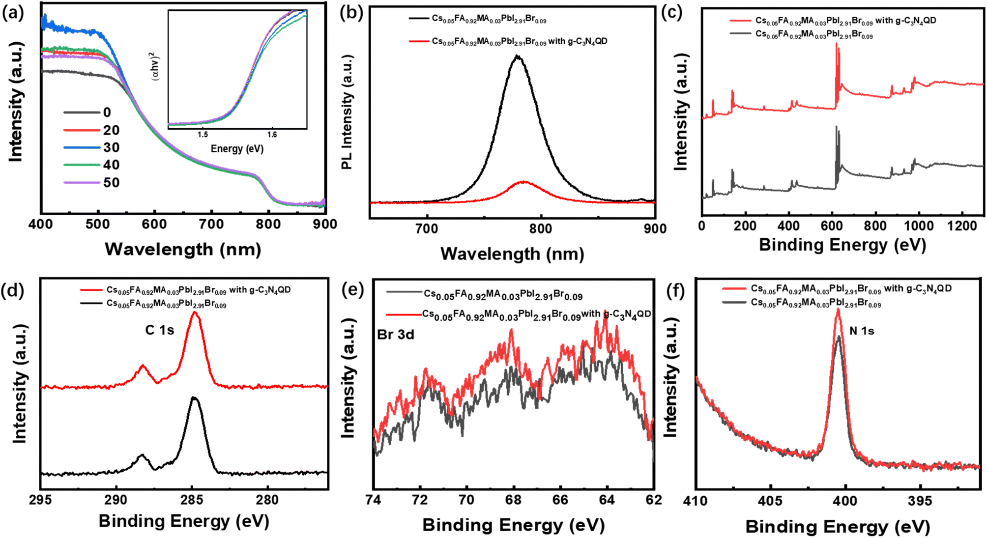
Fig. 1a shows the device configuration of the planar PSCs (FTO/PEDOT:PSS/perovskite/PCBM/BCP/Ag). PSCs bases on ABX3 (where A is MA+ and FA+, B is Pb2+ and Cs2+, X is Br− and I−) have become the most promising power source of all the solar cells because of their low manufacture cost, high open-circuit voltage (Voc) and excellent PCE. Fig. 1b and c show the top-view images of perovskite films without and with g-C3N4QDs deposited on PEDOT:PSS layer coated on FTO glass by using scanning electron microscopy (SEM) respectively. The increased interfacial contact angle shows highly hydrophobic of perovskite film with g-C3N4QDs, which created by the ordering growth of perovskite grains based on the introduction of g-C3N4QDs. Fig. 1c shows the size of perovskite cuboids increases with doping g-C3N4QDs and the morphology shows almost full surface coverage with larger grains in comparison with the control sample. Notably, both films with different doping ratios of g-C3N4QDs have denser and better uniform morphology (Fig. S1a–e†). The decreases of pinholes avoid the direct contact between PEDOT:PSS and PCBM, which suppress the electrons recombined with the holes. Fig. 1d shows the XRD of perovskite films based on g-C3N4QDs. It is obvious that the films fabricated from perovskite solutions in the absence and presence of g-C3N4QDs have a cubic perovskite phase with an almost unchanged crystal structure. The main peaks around 13.99° and 28.36° are corresponding to the (110) and (200) crystal plans, which confirms the perovskite structure of the as-prepared films has no difference. The morphology of perovskite films is associated with the crystallinity, the crystallization peak strength of films with g-C3N4QDs increased. Fig. 1d shows the similar crystal structure exhibit in these films, however, the difference is obvious in consideration of surface coverage and film conformity, which are well known to be the most significant parameters that affect device performance. Fig. 1e and f shows the AFM images of perovskite films with and without g-C3N4QDs incorporation. Compared to the pristine perovskite film, obviously improvement in film morphology was observed in g-C3N4QDs modified perovskite films. The root-mean-square value of perovskite film was determined to be 44.1 nm. It decreased to 29.3 nm after incorporating g-C3N4QDs (30%). The influence of other doping ratios on the surface morphology were shown in Fig. S1f–j,† respectively. The reduced roughness suggests a good interfacial contact between the perovskite layer and the upper electron-transporting layer.Fig. 2a displays the UV-Vis spectra of the perovskite layer doped with g-C3N4QDs. There is no large difference in the absorption wavelength range of the perovskite films in visible light range, however, the absorption of all peaks of the film with g-C3N4QDs enhanced among 400–550 nm. The bandgap of perovskite films with and without the g-C3N4QDs films are extrapolated from the optical absorption spectra as shown inside, which has no difference with the g-C3N4QDs employment. The band gaps of the perovskite films with and without the g-C3N4QDs can be extrapolate from the Tauc plot ((αhν)1/2 vs. eV). Fig. 2b shows the steady-state photoluminescence (PL) measurements to explore the recombination behaviors of photogenerated carriers in perovskite films with and without g-C3N4QDs. The normalized PL intensity increases with the doping of g-C3N4QDs, exhibiting the same tendency as the SEM results. This signifies that an appropriate amount of g-C3N4QDs can render perovskite films with reduced levels of nonradiative charge carrier recombination. The increased grain size and PL intensity of perovskite film show g-C3N4QDs can passivate the negative defects in the polycrystalline perovskite films. As a result, we believe that the proper amount of g-C3N4QDs addition is beneficial to obtain perovskites with favorable grains and lower trap densities, and the crystallinity increased obviously to some extent, the suppression of charge carrier recombination and reduced number of defect sites grant positive effects to enhance device performance. To investigate the influence of g-C3N4QDs on the electronic structure of perovskite film, X-ray photoemission spectroscopy (XPS) was employed to analyze the core levels of C/N/Br elements. As shown in Fig. 2c–f, the XPS survey spectrum of g-C3N4QDs clearly presented three peaks with different binding energy of 287.2 and 398.2 eV, corresponding to the core level of C 1s and N 1s, respectively. It is obviously that the binding energy of C, N elements have no changed, the hydroxylamine and carboxyl groups in g-C3N4QDs made the stronger element content of the corresponding elements. However, obvious change of Br 1s was observed after introducing g-C3N4QDs into the perovskite film. In addition, the bromine line (Br 3d) was also detected by the high energy resolution of XPS. To better understand the influence of g-C3N4QDs doping on the Br 3d core level, the deconvolutions of Br 3d spectra in the perovskite film was executed as shown in Fig. 2f. The Br 3d line can be resolved into two contributions, the Br 3d3/2 peak centered at 68.40 eV and Br 3d5/2 peak centered at 71.75 eV, implying the ionic state of Br in the sample. In addition, a shift was observed in the binding energies of the chemical states of Br 3d in the g-C3N4QDs modified perovskite film. The shift toward lower binding energy caused by the reduction property of hydroxylamine group in the g-C3N4QDs. The low binding energy indicates the g-C3N4QDs provides charge to the perovskite, which show higher relaxation energy contributed to electron kinetic energy. The high electron kinetic energy helps to improve the charge mobility.
 | ||
| Fig. 2 (a) The absorption spectrum of perovskite films without and with the optimized concentration of additive (30). (b) The steady-state photoluminescence spectrum of perovskite films perovskite films without and with the optimized concentration of additive (30) deposited on the PEDOT:PSS/FTO. (c) The XPS spectra of perovskite films without and with the optimized concentration of additive (30). (d–f) High-resolution XPS C 1s/Br 3d/N 1s spectra of perovskite films without and with the optimized concentration of additive (30). | ||
Furthermore, ultrafast transient absorption (TA) spectroscopy was employed to study the in-depth charge transfer dynamics in the perovskite films. By tracking the bleach recovery of the corresponding transitions, we can characterize the recombination of photogenerated carriers in perovskite films. As shown in Fig. 3a and b, a broad negative absorption feature peaking at 740 nm is observed in both perovskite film and doped g-C3N4QDs, nanowires, which is derived from the photogenerated electrons in perovskite film. The much stronger negative absorption of g-C3N4QDs (30%) engineered perovskite film suggests a higher concentration of photogenerated electrons. A transient absorption peak located at 740 nm is observed for both control and engineered perovskite film, indicating that the two films can be excited by NIR light. Besides, the transient absorption intensity at 740 nm decreases from 1 ps to 8 ns via recombination with multiple time constants. The faster decline of charge concentration in engineered perovskite film compared to control film reveals that the electron decay process can be slowed in engineered perovskite film. Moreover, the explicit expression for the electron decay kinetics at 740 nm is calculated in detail. Fig. 3c shows transient fluorescence spectrum exported from TA curves, the fitted time profiles exhibit the delay time of engineered perovskite film (1274.93 ps) longer than that for control film (828.38 ps). Accordingly, the above results confirm that the introduction of g-C3N4QDs doping are favorable for the prolonged lifetime of photogenerated electrons. To uncover the effect of g-C3N4QDs on the electronic structures of perovskite, the Nuclear Magnetic Resonance (NMR) of H was carried out. Fig. 3d shows the 1H-NMR of perovskite films without and with g-C3N4QDs. The DMSO-d6 used as liquid-state NMR solvent can avoid the influence of 1H-NMR signals of solvent on the samples. The peaks originated from the solvent were marked in the figure. Fig. 3e shows a magnification of the scale between 7 and 10 ppm. The broad peak at (a) belongs to protons of the FA amine groups, (b) belongs to CH of FA. A downshift (larger chemical shift) was clearly reflected at point (a) and (b) under the condition of g-C3N4QDs modified, which attributed to the inductive effect of hydroxylammonium groups in g-C3N4QDs causes electron density of FA in perovskite precursor solution to change. The downshift reflects a lower electron density induced by electron-attracting groups in the FA amine groups, which suppressed the electron energy loss and nucleate pace in the perovskite crystallization process. The broad peak between 2 and 4 ppm belongs to MA of perovskite, the same downshift also reflects the g-C3N4QDs induction as shown in Fig. 3f.
 | ||
| Fig. 3 (a) TA spectra of perovskite films with different g-C3N4QDs doping ratios at 589 fs Normalized kinetic traces after excitation at 460 nm. (b and c) TA spectra of perovskite films without and with the optimized concentration of additive (30) at 1 ps. (d) Liquid-state 1H magnetic resonance (NMR) spectra of (a) perovskite precursor solutions with and without g-C3N4QDs (DMF) in deuterated N,N-dimethylformamide-d7 (DMF-d7) and (e) magnification of the scale between 7 and 10 ppm, (f) 2–4 ppm. | ||
The current density–voltage (J–V) characteristics of the fabricated PSCs are carried out under simulated AM 1.5 sunlight conditions, as shown in Fig. 4a. The device based on g-C3N4QDs (30) shows a high PCE of 20.02%, with a Jsc of 25.93 mA cm−2, a Voc of 0.99 V, a FF of 0.78, and the PSC without the presence of g-C3N4QDs shows a PCE of 17.19%, with a Jsc of 23.95 mA cm−2, a Voc of 0.97 V, a FF of 0.74 (Table 1). Further increasing the g-C3N4QDs content deteriorates the device performance due to the reduced Jsc and FF. The increased Jsc benefitted from reduced surface defects and enlarged grains, which indicates that a compact interface contact is assumed to be formed between perovskite layer and ETL This fact is favorable for the suppression of shunting paths in the device and benefits the electron extraction, resulting in an enhanced FF. The increase in FF is primarily ascribed to the reduction of surface recombination and the enhancement of the charge collection efficiency. Fig. 4b shows the external quantum efficiency (EQE) of the reference and doped with g-C3N4QDs PSCs. It can be observed that EQE is improved all over the spectra from 300 to 850 nm in the g-C3N4QDs based PSCs. The integrated Jsc from the EQE spectra is around 24.51 mA cm−2 of PSC with g-C3N4QDs (30 μl), close to the Jsc obtain from the J–V sweep measurement, confirming the accuracy of device efficiency characterizations. To test the effect of g-C3N4QDs (30) on the device stability, Fig. 4S† shows the PCE decay trend of contrastive experiment devices with RH = 30%. The device with g-C3N4QDs (30) shows the slow decay compared to the control device under uninterrupted 120 hours testing process. The improved PCE stability in device with g-C3N4QDs (30) is considered of benefits from suppressed surface recombination and higher charge collection efficiency.
 | ||
| Fig. 4 (a) J–V curves of the devices without and with the optimized concentration of additive (30). (b) EQE spectra and their integrated current densities. (c) OCVD curves of the PSCs without and with the optimized concentration of additive (30). (d) Dark current–voltage curves of devices with different doping ratios. (e) Evolution of trap density during devices with different doping ratios. (f) Hole-only devices without and with the optimized concentration of additive (30) with the structure shown in the inset. | ||
| Devices | Voc (V) | Jsc (mA cm−2) | FF (%) | PCE (%) |
|---|---|---|---|---|
| Perovskite | 0.97 | 23.95 | 0.74 | 17.19 |
| Perovskite-g-C3N4QDs (0.2 wt%) | 0.98 | 25.04 | 0.76 | 18.64 |
| Perovskite-g-C3N4QDs (0.4 wt%) | 0.99 | 25.93 | 0.78 | 20.02 |
| Perovskite-g-C3N4QDs (0.6 wt%) | 1.00 | 24.81 | 0.76 | 19.08 |
| Perovskite-g-C3N4QDs (0.8 wt%) | 1.00 | 24.62 | 0.72 | 17.62 |
We ascribed it to a passivation effect of g-C3N4QDs with flat perovskite surface and good interface contact with upper layer component. Electrochemical impedance spectrum (EIS) is an effective method to provide rich interfacial information such as contact resistance in multilayer devices. Fig. 4c gives the Nyquist plots of both devices in the dark at an applied voltage of 0.95 V. The series resistance (Rs), transport resistance (Rtr) and composite resistance (Rrec) could be extrapolated by employing an equivalent circuit model composing of Rs, Rtr, Rrec and parallel capacitor C. The Nyquist plots have two round arcs of devices without and with g-C3N4QDs. The modified device has a reduced radius of the first round arc at high frequency, which demonstrates that g-C3N4QDs doping reduced the carrier transfer resistance and optimized the contact interface. There are pretty clear differences between the second round arc at low frequency. The increased radius demonstrates that g-C3N4QDs doping enlarged the carries composite resistance, which means lower carries recombination loss. Fig. 4d shows the (J–V) characteristics in the dark of devices without and with g-C3N4QDs in different proportions. The higher dark current density indicates more carriers in the region has been consumed by defects in the perovskite film and device. The lower dark current density indicates g-C3N4QDs-passivation decreased the scattering centers of the carriers at the grain boundaries, thus, increased the Hall mobility of the carriers. The shift up of dark current density induced by more carries recombination with the increase of g-C3N4QDs doping density. To explore the formation of defects influence on the performance of the solar cells, we conducted defect density measurement to understand what caused the degradation of devices under dark illumination. Fig. 4e shows trap energy level and the energetic profile of trap density of states (tDOS) of PSCs. It was found that g-C3N4QDs caused a reduced trap density with energy depth of 0.25 to 0.45 eV, where the charge traps are caused by the recombination of carriers in perovskites. The reduction of deep traps can be explained by the reduction of amorphous regions during annealing, which benefits from the forming of passivation interface doped with g-C3N4QDs. It is consistent with morphology study in terms of increased grain size during annealing.
To confirm the effect of g-C3N4QDs additive to the charge transporting of PSCs, the space charge limited current (SCLC) region can reflect the efficient charge transfer of device. Fig. 4f shows the J–V characteristics of perovskite films without and with the g-C3N4QDs based on hole-only devices with a structure of FTO/PEDOT:PSS/Cs0.05FA0.92MA0.03PbI2.91Br0.09/Spiro-OMeTAD/MoO3/Ag. The hole-only devices were tested under the dark condition different from the optimized photovoltaic devices. The electron and hole mobilities (μ) can be calculate according to Mott–Gurney's equation as follows. Where the values of ε0 (the vacuum permittivity) and εr (material dielectric constant) are 8.8542 × 10⁻¹⁴ F cm−1 and 6.5, respectively, μ is the electron/hole mobility and L is the perovskite layer thickness. Comparing to the control one, the hole mobility enhanced obviously by doping of g-C3N4QDs. The hole mobilities of devices based on perovskite and perovskite with g-C3N4QDs films are calculated by the equation, which are 7.23 × 10⁻³ and 9.48 × 10⁻³ cm2 V−1 S−1 of perovskite with g-C3N4QDs film, respectively.
High-quality crystal in the perovskite films is key to carriers transmission between each layer in good ohmic contact, as previously mentioned, which allows for a more smooth of intermolecular charge transfer and hence a higher charge carrier mobility. The results are accord well with the time-resolved photoluminescence (TRPL) spectra (Fig. S2†). Which shows comparation of with and without the g-C3N4QDs films deposited on the electron-transporting layer. The PL decay spectra were fitted into a biexponential decay function consisting of two times intervals, corresponding to a fast and a slow decay process. The fast decay process is associated with the quenching of free carriers in the perovskite domain through the charge transfer to the HTL, and the slow decay process is related to the radiative decay. The fast decay time indicating a charge-transfer dominant decay mechanism. Fig. S3† shows Hall effect measurement dependence of carrier density and Hall mobility of perovskite film. The higher carrier density of perovskite-g-C3N4QDs film benefits from the compact and flat surface. In addition, the Hall mobility in the perovskite-g-C3N4QDs film compared with the pristine perovskite film exhibits a larger value. This means that g-C3N4QDs doped perovskite film possess good conductivity, which enables corresponding PSCs to have a better device performance.
Conclusion
In summary, we demonstrated the effect of g-C3N4QDs on the performance of PSCs and investigated the action mechanism of the morphology, carrier mobility and interface electrical characteristic of perovskite film. The PCE of g-C3N4QDs based PSCs demonstrated a power conversion efficiency as high as 20.02% with simultaneous improvements of Jsc (23.95 to 25.93 mA cm−2) and FF (0.74 to 0.78). The improved performance of PSCs benefits from high carrier mobility and reduced defects of perovskite film. The larger grains and uniform morphology of perovskite film also reduced series resistance and charge recombination chance.Conflicts of interest
There are no conflicts to declare.Acknowledgements
We acknowledge financial support from the Youth Science Foundation of Henan Province (No. 202300410239) (232300421372) and from the Department of Education Project – Henan Province, the Basic Research Project of Key Scientific Research Project (No. 21A430023). This project is also funded by the Key Research & Development and Promotion Projects of Henan Province (232102241017).References
- P. G. V. Sampaioa and M. O. A. González, Renew. Sustain. Energy Rev., 2017, 74, 590 CrossRef.
- H. P. Zhou, Q. Chen, G. Li, S. Luo, T. B. Song, H. S. Duan, Z. Hong, J. You, Y. Liu and Y. Yang, Science, 2014, 345, 542 CrossRef CAS PubMed.
- M. A. Green, A. Ho-Baillie and H. J. Snaith, Nat. Photonics, 2014, 8, 506 CrossRef CAS.
- J. Luo, R. He, H. Lai, C. Chen, J. Zhu, Y. Xu, F. Yao, T. Ma, Y. Luo, Z. Yi, Y. Jiang, Z. Gao, J. Wang, W. Wang, H. Huang, Y. Wang, S. Ren, Q. Lin, C. Wang, F. Fu and D. Zhao, Adv. Mater., 2023, 24, 2300352 CrossRef PubMed.
- Y. H. Chen, N. X. Li, L. G. Wang, P. F. Liu, W. Zou, G. C. Xing, X. F. Liu, J. P. Wang, D. D. Li, B. L. Huang, Q. Chen and H. P. Zhou, Nat. Commun., 2019, 10, 1112 CrossRef PubMed.
- Z. J. Yong, S. Q. Guo, J. P. Ma, J. Y. Zhang, Z. Y. Li, Y. M. Chen and H. T. Sun, J. Am. Chem. Soc., 2018, 140, 9942 CrossRef CAS PubMed.
- H. L. Wu, C. Z. Xu, Z. Kang, Z. Z. Xiong and Y. Zhang, Nano Lett., 2022, 22, 1467 CrossRef CAS PubMed.
- Y. K. Xu, M. Wang, Y. T. Lei, Z. P. Ci and Z. W. Jin, Adv. Energy Mater., 2020, 10, 2002558 CrossRef CAS.
- J. Li, W. F. Pan, Q. Y. Liu, Z. Q. Chen, Z. J. Chen, X. Z. Feng and H. Chen, J. Am. Chem. Soc., 2021, 143, 6551 CrossRef CAS PubMed.
- T. Y. Zhao, Z. P. Xing, Z. Y. Xiu, Z. Z. Li, S. L. Yang and W. Zhou, ACS Appl. Mater. Interfaces, 2019, 11, 7104 CrossRef CAS PubMed.
- A. Kausar, A. Sattar, C. Z. Xu, S. C. Zhang, Z. Kang and Y. Zhang, Chem. Soc. Rev., 2021, 50, 2696 RSC.
- F. Ye, J. Ma, C. Chen, H. Wang, Y. Xu, S. Zhang, T. Wang, C. Tao and G. Fang, Adv. Mater., 2020, 33, 2007126 CrossRef PubMed.
- Y. P. Zhao, I. Yavuz, M. H. Wang, M. J. Xu, J. H. Lee, N. G. Park, J. W. Lee and Y. Yang, Nat. Mater., 2022, 21, 1396 CrossRef CAS PubMed.
- C. Cho, S. Feldmann, K. M. Yeom, Y. W. Jang, S. D. Stranks and N. C. Greenham, Nat. Mater., 2022, 21, 1388 CrossRef CAS PubMed.
- Y. Zhang, T. F. Kong and D. Q. Bi, ACS Energy Lett., 2022, 7, 929 CrossRef CAS.
- Z. C. Shen, Q. F. Han and L. Y. Han, Energy Environ. Sci., 2022, 15, 1078 RSC.
- S. Zhan, Y. W. Duan, Z. K. Liu, L. Yang, K. He and S. Z. Liu, Adv. Energy Mater., 2022, 12, 2200867 CrossRef CAS.
- W. J. Chen, S. Liu and Y. F. Li, Adv. Mater., 2022, 5, 2110482 CrossRef PubMed.
- Y. F. Wang, B. Y. Jia, X. W. Zhan, 2020, 29, 2002066.
- L. W. Tian, F. Wen, W. F. Zhang, H. C. Zhang, Y. T. Jiang, M. Zhang and Y. L. Huang, ACS Appl. Mater. Interfaces, 2020, 12, 49648 CrossRef CAS PubMed.
- L. L. Jiang, Z. K. Wang, M. Li, C. C. Zhang, Q. Q. Ye, K. H. Hu, D. Z. Lu, P. F. Fang and L. S. Liao, Adv. Funct. Mater., 2018, 28, 1705875 CrossRef.
- C. H. Chiang, M. K. Nazeeruddin, M. Gratzel and C. G. Wu, Energy Environ. Sci., 2017, 10, 808 RSC.
- J. W. Yin, Z. F. Xu, Q. Hu, L. M. Liu and O. V. Prezhdo, J. Am. Chem. Soc., 2023, 145, 5393 CrossRef CAS PubMed.
- T. Yuan, F. L. Yuan, L. Z. Sui, Y. Zhang, Y. C. Li and L. Z. Fan, Angew. Chem., Int. Ed., 2023, 135, 18568 Search PubMed.
- H. R. Sun, S. L. Wang, S. S. Qi, P. Y. Wang and X. D. Zhang, Adv. Funct. Mater., 2023, 2213913 CrossRef.
- J. Xiang, C. Han, J. Qi, Y. Cheng, K. Chen, Y. Ma, J. Xie, Y. Hu, A. Mei, Y. Zhou and H. Han, Adv. Funct. Mater., 2023, 2300473 CrossRef.
- W. Hui, X. X. Kang, B. H. Wang, D. L. Li, L. Song and W. Huang, Nano Lett., 2023, 23, 2195 CrossRef CAS PubMed.
- C. Liu, K. Huang, B. Hu, Y. Li, L. Zhang, X. Zhou, Y. Liu, Z. Liu, Y. Sheng, S. Chen, X. Wang and B. Xu, Adv. Funct. Mater., 2023, 2212698 CrossRef CAS.
- Q. Zhou, B. B. Liu, X. X. Shai, Y. L. Li, Z. X. Xu, D. Wei and J. Z. Chen, Chem. Commun., 2023, 59, 4128 RSC.
- Q. H. Lin, Y. B. Zhu, Y. Wang, Y. Liu, F. S. Li and W. Huang, Adv. Mater., 2023 DOI:10.1002/adma.202210385.
- T. H. Wu, X. S. Xu, L. K. Ono, T. Guo, A. Narita and Y. B. Qi, Adv. Mater., 2023, 35, 2300169 CrossRef CAS PubMed.
- J. P. Wu, M. H. Li, J. T. Fan, Z. B. Li, D. J. Xue and J. S. Hu, J. Am. Chem. Soc., 2023, 145, 5872 CrossRef CAS PubMed.
- R. Yadav, Y. Kwon, C. Rivaux and P. Reiss, J. Am. Chem. Soc., 2023, 145, 5970 CrossRef CAS PubMed.
- J. T. Wang, M. A. Uddin, B. Chen, X. J. Ying, Z. Y. Ni, Y. Zhou, M. Z. Li and J. S. Huang, Adv. Energy Mater., 2023, 2204115 CrossRef CAS.
- C. W. Li, X. M. Wang, E. B. Bi, Z. N. Song and Y. F. Yan, Science, 2023, 379, 690 CrossRef CAS PubMed.
- M. L. Sun, J. F. Shu, C. X. Zhao, J. P. Wu, X. Yin, Z. A. Tan, M. He and L. Y. Wang, ACS Appl. Mater. Interfaces, 2022, 14, 3352 Search PubMed.
- X. Lin, Z. Z. Xu, Y. J. Guo, P. Xu and M. He, ACS Appl. Mater. Interfaces, 2016, 8, 29580 CrossRef PubMed.
- X. Yin, Y. J. Guo, Z. S. Xue, P. Xu, M. He and B. Liu, Nano Res., 2015, 8, 1997 CrossRef CAS.
- W. J. Yu, C. J. Liu, X. R. Sun, T. Hou, X. Yang, Y. L. Huang and M. Zhang, Nano Res., 2023, 16, 521 CrossRef CAS.
- Y. H. Ma, H. Y. Zhang, Y. W. Zhang, R. Y. Hu, M. Jiang, R. D. Xia, X. A. Li and W. Huang, ACS Appl. Mater. Interfaces, 2019, 11, 3044 CrossRef CAS PubMed.
Footnote |
| † Electronic supplementary information (ESI) available. See DOI: https://doi.org/10.1039/d3ra02391e |
| This journal is © The Royal Society of Chemistry 2023 |