 Open Access Article
S,N-GQD sensitization effect on the improvement of ZnO nanopencil photoelectrochemical properties†
Allyn Pramudya Sulaeman *a,
Rifky Adhia Pratama
 a,
Uji Pratomo
 a,
Irkham
 a,
Avtar S. Matharu
 b and
Indah Primadona
 *cd
*cd
aDepartment of Chemistry, Faculty of Mathematics and Natural Sciences, Universitas Padjadjaran, Sumedang, 45363, Indonesia
bGreen Chemistry Centre of Excellence, Department of Chemistry, University of York, York YO10 5DD, UK
cResearch Center for Advanced Material, National Research and Innovation Agency, Kawasan Puspiptek, Banten 15314, Indonesia. E-mail: inda009@brin.go.id
dCollaboration Research Center for Advanced Energy Material, National Research and Innovation Agency-Institut Teknologi Bandung, Indonesia
First published on 19th June 2023
Abstract
ZnO photoanodes in photoelectrochemical (PEC) water splitting for green-hydrogen production are limited due to the large bandgap that is only confined to UV light. One of the strategies for broadening the photo absorption range and improving light harvesting is to modify a one-dimensional (1D) nanostructure to a three-dimensional (3D) ZnO superstructure coupling with a narrow-bandgap material, in this case, a graphene quantum dot photosensitizer. Herein, we studied the effect of sulfur and nitrogen co-doped graphene quantum dot (S,N-GQD) sensitization on the surface of ZnO nanopencil (ZnO NPc) to give a photoanode in the visible light spectrum. In addition, the photo energy harvesting between the 3D-ZnO and 1D-ZnO, as represented by neat ZnO NPc and ZnO nanorods (ZnO NRs), was also compared. Several instruments, including SEM-EDS, FTIR, and XRD revealed the successful loading of S,N-GQDs on the ZnO NPc surfaces through the layer-by-layer assembly technique. The advantages are S,N-GQDs's band gap energy (2.92 eV) decreasing ZnO NPc's band gap value from 3.169 eV to 3.155 eV after being composited with S,N-GQDs and facilitating the generation of electron–hole pairs for PEC activity under visible light irradiation. Furthermore, the electronic properties of ZnO NPc/S,N-GQDs were improved significantly over those of bare ZnO NPc and ZnO NR. The PEC measurements revealed that the ZnO NPc/S,N-GQDs stood out with a maximum current density of 1.82 mA cm−2 at +1.2 V (vs. Ag/AgCl), representing a 153% and 357% improvement over the bare ZnO NPc (1.19 mA cm−2) and the ZnO NR (0.51 mA cm−2), respectively. These results suggest that ZnO NPc/S,N-GQDs could have potential for water splitting applications.
Introduction
Human energy demands have risen dramatically in recent years. As a result, the development of novel energy conversion and storage strategies based on renewable and sustainable energy sources has been prioritized.1–3 Particularly, allowing the solar cell to effectively capture approximately 43% of the sun's visible light reaching the ground. In the same context, PEC water splitting for green-hydrogen generation utilizing semiconductors has gained popularity due to its environmental friendliness.2,4–7ZnO is considered as an essential semiconductor for PEC water splitting because of its high efficiency and inexpensive cost. Due to their remarkable physicochemical features, ZnO superstructures have produced astounding achievements in PEC.8–10 “Superstructures” are 3D geometries composed of controlled morphology and crystal orientation 1D and 2D nanostructures. Superstructures provide exceptional key features such as high crystallinity, ordered and integrated arrangement with recurring regularity, high surface area, good electrical conductivity, high optical absorption, and so on, which overcome the drawbacks of 1D and 2D nanostructures.11–15 Consequently, superstructures of various semiconductors have demonstrated remarkable photocatalytic efficacy, gas sensing, energy conversion and storage devices, and other applications.16–18
Lv et al. informed the outstanding PEC water splitting performance of ZnO NPc superstructure.19 The photocurrent density produced by the ZnO NPc arrays is approximately 1.3 mA cm−2 at 1 V against Ag/AgCl under 100 mW cm−2 (AM 1.5) visible light illumination, which is double that of the ZnO NR arrays. According to previous reports, the existence of long-tip on the top ZnO NR could enhance the electrical properties due to a high oxygen-vacancy concentration.19–22 However, constructing a photoanode with high stability and efficiency is difficult due to the fact that most ZnO materials have a large band gap and suffer from severe electron–hole pair recombination.23
Graphene quantum dots (GQDs) as zero-dimensional (0D) graphene derivatives with sp2 hybridization are a strong candidate for sensitizing the photoelectrochemical performance of ZnO under visible light irradiation.24 Subsequent to the energy absorption, the high electron density of quantum dots material will cause electron transfer from its LUMO (Lowest Unoccupied Molecular Orbital) level to the semiconductor acceptor's conduction band (CB) to carry out the water-to-hydrogen reduction process.25–28 After being composited with nitrogen co-doped GQDs, Zeng et al. found that the ZnO nanowires IPCE (Incident Photon-to-current Conversion Efficiency) increased from 0.017% to 0.29%.29
Recently, S,N-GQDs have also received attention due to their visible photo absorption, strong carrier transport mobility, and outstanding chemical stability.30 Xie et al. and Cai et al. have successfully combined S,N-GQDS with TiO2 and ZnO nanoparticles, and they found an improvement in the visible light absorption and photogenerated e−/h+ separation.31,32 Given its potential to enhance photocatalytic activity, further exploring this material to sensitize high-active-surface 3D ZnO nanostructures for water splitting application becomes interesting. Herein, we successfully synthesized ZnO NPc/S,N-GQDs heterostructure composite electrodes through Layer-by-Layer (LbL) assembly technique. ZnO NPc superstructure arrays and S,N-GQDs with citric acid as a carbon source and thiourea as a sulfur and nitrogen atom precursor were prepared by hydrothermal method. In this study, we examined and compared the optical and photoelectrochemical performance of this novel sensitization material of ZnO NPc/S,N-GQDs with the bare ZnO NR and ZnO NPc arrays. Furthermore, the possible mechanism of the photocatalytic process driven by ZnO NPc/S,N-GQDs was also proposed.
Experimental
Materials
All analytical-grade sodium hydroxide (97%), ethanol (>99%), citric acid (C6H8O7), thiourea (CH4N2S), zinc acetate dihydrate (ZAD), zinc nitrate hexahydrate (ZNH), hexamethylenetetramine (HMTA), polyethylenimine (PEI), sodium sulphate (Na2SO4), and the fluorine-doped tin oxide (FTO) conductive glass substrates having sheet resistance around 10–14 Ω cm−2 were purchased from Sigma-Aldrich, Merck, KGaA, Darmstadt, Germany. All solutions were made with deionized water that had been doubly distilled.Fabrication of ZnO NPc/S,N-GQDs composite
Firstly, S,N-GQDs was prepared by applying the hydrothermal method. Briefly, citric acid (2.5168 g, 1 mmol) and thiourea (4.9859 g, 5 mmol) were dissolved in 60 mL of water, followed by stirring until a clear solution was observed. Afterward, the clear solution was sealed in a 50 mL Teflon-lined autoclave and heated hydrothermally at 160 °C for 8 hours. Then, the autoclave was taken out and cooled to room temperature. Finally, the obtained yellow solution of S,N-GQDs was purified by centrifugation at 6500 rpm for 15 min to get a dark green precipitate (S,N-GQDs).Secondly, ZnO NPc superstructure was made by starting the seed preparation on FTO glass substrate through Ultrasonic Spray Pyrolysis (USP) technique. A seed solution (0.2 M of ZAD solution) was put into the atomic nebulizer chamber, and the USP process was conducted for about 15 minutes and continued with the annealing process (1 hour). The FTO glass substrate with the ZnO seed on top of it was then grown to a nanorod array by hydrothermal method. About 10 mL of a 0.1 M ZNH and 0.1 M HMTA mix solution (1![[thin space (1/6-em)]](https://www.rsc.org/images/entities/char_2009.gif) :
:![[thin space (1/6-em)]](https://www.rsc.org/images/entities/char_2009.gif) 1 v/v) was poured into a mini vial and then put into an oven with a 95 °C hydrothermal temperature for 6 h. The obtained ZnO NR was then thoroughly rinsed with deionized water and dried in air. To develop the desired ZnO NPc superstructures, a ZnO NR was placed downward near the surface of the reaction solution (vial) filled with a mixture solution (9 mL of 5 mM ZNH & HMTA and 0.1875 mM of ascorbic acid) and heated to T = 90 °C for 8 h. After the reaction, the samples were cleaned with deionized water and dried at 80 °C.
1 v/v) was poured into a mini vial and then put into an oven with a 95 °C hydrothermal temperature for 6 h. The obtained ZnO NR was then thoroughly rinsed with deionized water and dried in air. To develop the desired ZnO NPc superstructures, a ZnO NR was placed downward near the surface of the reaction solution (vial) filled with a mixture solution (9 mL of 5 mM ZNH & HMTA and 0.1875 mM of ascorbic acid) and heated to T = 90 °C for 8 h. After the reaction, the samples were cleaned with deionized water and dried at 80 °C.
Finally, ZnO NPc/S,N-GQDs was fabricated using LbL technique. The ZnO NPc was dipped into PEI aqueous solution (1.0 mg mL−1, 0.5 M NaCl, pH = 7.23) for 10 min and washed three times with deionized water, followed by drying with a gentle stream of N2. Subsequently, the resultant substrate was immersed in S,N-GQDs aqueous suspension (1.0 mg mL−1, pH = 6.89) for 10 min, rinsed with deionized water and dried by a stream of N2. ZnO NPc/S,N-GQDs heterostructure was then calcined in a nitrogen atmosphere at 400 °C for 1 h at a heating rate of 5 min−1.
Characterization
The structure and morphology of the samples were characterized by a wide range of instruments. The crystal phase purity of various ZnO structures were investigated by X-ray diffraction (XRD) analyses using Bruker D8 Advance (Germany), with Cu-Kα (λ = 1.54 Å) X-ray source. Raman spectra were recorded on iHR320 HORIBA. The optical properties of all samples were investigated by Lambda 950 UV/Vis/NIR (PerkinElmer) and Diffuse Reflectance Spectroscopy (DRS) instrument Jena Specord 210 Plus 190. Morphological analyses of the samples were investigated by Scanning Electron Microscopic (SEM) analysis using JEOL JSM IT-300LV (Japan), combined with Energy Dispersive X-ray (EDX) spectroscopy. The functional group of materials were scanned by Fourier Transform Infra-Red (FTIR) Nicolet 6700 Thermo Fisher. The fluorescence emission spectra of all samples were carried out using Hitachi F-2700 fluorophotometer spectroscopy to identify charge recombination and crystal defects on the samples.Photoelectrochemical (PEC) measurement
PEC measurements for water splitting were performed in a standard three-electrode electrochemical cell configuration, using the as-prepared ZnO NR, ZnO NPc, and ZnO NPc/S,N-GQDs composites on FTO glass as the working electrode, a platinum wire as the counter electrode, and Ag/AgCl as the reference electrode. A 0.5 M Na2SO4 solution buffered to pH ∼7.0 with phosphate buffer solution was employed as the electrolyte and purged with N2 for 5–10 min before the measurements. The PEC measurements (linear sweep voltammetry and chronoamperometry) were recorded under AM 1.5 G illumination from a solar simulator (100 mV cm−2, Iwasaki Solar Simulation Evaluation Systems equipped with EYE/Iwasaki electronic ballast system). The potential measured against an Ag/AgCl reference electrode.Result and discussion
Characterization of ZnO NPc/S,N-GQDs heterostructure composite
In this study, the ZnO NPc structures with a long rod as a “pencil holder” and a cone-like tip was effectively synthesized by a hydrothermal approach following the previous work by Lv et al. with some modification at the ZnO seed layer deposition process on top of an FTO glass substrate using the USP technique.19 The schematic diagram of the construction of ZnO NPc arrays from ZnO NR is shown in Fig. 1a. One dimensional-ZnO NRs grow along the c-axis of a wurtzite crystal, but the existence of ascorbic acid was effectively utilized to inhibits the crystal growth in the edge of the ZnO NR [100] direction. This phenomenon is crucial for the creation of the tip of the ZnO NPc.22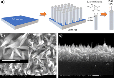 | ||
| Fig. 1 (a) Schematic illustration of ZnO NPc construction, SEM image of (b) ZnO NPc, and (c) cross-sectional view of ZnO NPc. | ||
The Scanning electron microscopy (SEM) was used to examine the morphology of the as-prepared ZnO NPc arrays. Highly homogeneous and dense ZnO NR and NPc arrays were almost perpendicular to the surface of the FTO substrate, as illustrated in Fig. 1b and c. The pencil tip was growing atop each nanorod with an average width of 70.85 nm and an average length of 150 nm provided in Fig. S1a and b.† The average width (163.13 nm) and height (319.95 nm) of ZnO NR as a pencil holder, as estimated by the ImageJ program also depicted in Fig. S1c and d.†
S,N-GQDs were successfully synthesized using the hydrothermal method. Based on Qu et al. studies, there are three steps involved in S,N-GQDs formation. The citric acid molecules initially self-assemble, and nanosheet structures develop as a result of intermolecular H-bonding. The GQDs and various carboxyl also hydroxyl groups are created during the de-hydrolysis step. During the hydrothermal process, S and N atoms are covalently bound with carbon atoms by the interaction of thiourea molecules, and S, N co-doped GQDs (S,N-GQDs) are produced.33
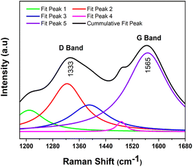
As shown in the Fig. 2, the Raman spectra demonstrate the high quality of the as-prepared co-doped sulfur and nitrogen GQDs. S,N-GQDs exhibit the disordered (D) band at 1333 cm−1, which is attributed to the existence of sp3 defects, and the crystalline (G) band at 1565 cm−1, which is associated with sp2 carbon in-plane vibration. These distinctive bands' intensity ratio (ID/IG) can be utilized to correlate the carbon's structural features. In this study, the ID/IG ratio of the S,N-GQDs is around 0.77.
The optical properties of S,N-GQDs were characterized by UV/Vis spectroscopy as depicted in Fig. 3a, which displays broad absorption bands centered at 625 nm. The wide bands between 450–700 nm may be attributed to the n → π* transition of the conjugated C![[double bond, length as m-dash]](https://www.rsc.org/images/entities/char_e001.gif) N and C
N and C![[double bond, length as m-dash]](https://www.rsc.org/images/entities/char_e001.gif) S bonds and to the π → π* of S
S bonds and to the π → π* of S![[double bond, length as m-dash]](https://www.rsc.org/images/entities/char_e001.gif) O bond.34 These are in accordance with the product's color, where a dark green solution was observed.
O bond.34 These are in accordance with the product's color, where a dark green solution was observed.
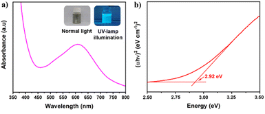 | ||
| Fig. 3 (a) UV/Vis spectra of S,N-GQDs (the left inset is S,N-GQDs suspension in normal light while the right inset is under UV-lamp illumination), and (b) Tauc plot of S,N-GQDs. | ||
The optical direct band gap value of S,N-GQDs could be determined using the Tauc's formula (αhv)2 = α0(hv − Eg) where h, α0, and Eg denote photon energy, a constant, and optical band gap, respectively.32 The use of linear extrapolation makes it straightforward to arrive at a gap energy of 2.92 eV for the S,N-GQDs' direct band gap, as shown in Fig. 3b. The S,N-GQDs have a lower Eg than well-known ZnO (3.4 eV),35 resulting in a bandgap difference of 0.48 eV, allowing S,N-GQDs to be able as a potential sensitizer for ZnO.36
To evaluate the success of the LbL process for producing ZnO NPc/S,N-GQDs heterostructure composites, all samples were characterized by FTIR, XRD, XPS, and SEM-EDX. FTIR spectra (Fig. 4a) reveal the O–H bending vibration, the stretching peak of S–CN, the stretching C![[double bond, length as m-dash]](https://www.rsc.org/images/entities/char_e001.gif) C
C![[double bond, length as m-dash]](https://www.rsc.org/images/entities/char_e001.gif) C, and the bending mode of C
C, and the bending mode of C![[double bond, length as m-dash]](https://www.rsc.org/images/entities/char_e001.gif) C at 3463, 2156, 1974, and 961 cm−1, respectively, which confirmed the success of loaded S,N-GQDs onto ZnO NPc. In addition, the following characteristic ZnO NPc/S,N-GQDs FTIR peaks originated from ZnO NPc, H–O–H vibration and Zn–O bending at 2358 and 664 cm−1, respectively, were detected.
C at 3463, 2156, 1974, and 961 cm−1, respectively, which confirmed the success of loaded S,N-GQDs onto ZnO NPc. In addition, the following characteristic ZnO NPc/S,N-GQDs FTIR peaks originated from ZnO NPc, H–O–H vibration and Zn–O bending at 2358 and 664 cm−1, respectively, were detected.
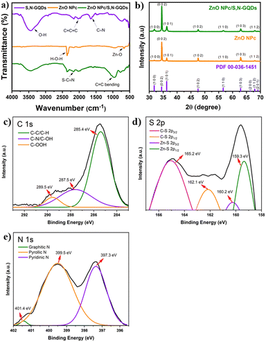 | ||
| Fig. 4 (a) FTIR spectra, (b) XRD pattern, high resolution XPS spectra of (c) C 1s, (d) S 2p, and (e) N 1s core elements. | ||
The crystalline characteristics of ZnO NPc/S,N-GQDs produced on FTO substrates were studied using X-ray diffraction techniques, as shown in Fig. 4b. The XRD results show that our as-grown ZnO NPc is highly crystalline. The hexagonal wurtzite structure of ZnO is thought to be responsible for the dominating diffraction peaks at the (100), (002), (101), (102), (110), (103), and (102) planes based on JCPDS card no. 00-036-1451 (space group: P63mc with lattice constants a and b = 3.249 Å and c = 5.206 Å). It should be noted that the crystal structure did not significantly change following the attachment of S,N-GQDs. It aligns with the clean SEM image of the final ZnO NPc/S,N-GQDs (Fig. S2a†) showing that the nanopencil structure still exists after sensitization process. The components of S,N-GQDs and ZnO NPc in a composite heterostructure can be identified using an SEM instrument, and elemental mapping (Fig. S2†) showed that C, S, and N atoms were present on the ZnO NPc matrix in a uniform distribution. The specific atomic percent of each atom is listed in Table S1.†
To study the possible interaction between ZnO NPc and S,N-GQDs, XPS characterization was carried out for ZnO NPc/S,N-GQDs heterostructure composites. The survey XPS spectrum (Fig. S3a†) of the ZnO NPc/S,N-GQDs heterostructure is primarily composed of Zn 2p, O 1s, C 1s, S 2p, and N 1s, indicating that the S,N-GQDs were successfully deposited on the ZnO NPc. The Zn 2p spectrum (Fig. S3b†) has one doublet peak at 1022.4 eV (Zn 2p3/2) and 1045.4 eV (Zn 2p1/2). The high-resolution O 1s, C 1s, S 2p, and N 1s spectra of the ZnO NPc/S,N-GQDs heterostructure can be deconvoluted into several Gaussian peaks that correspond to various types of functional groups. Two peaks at 530.6 and 532.1 eV are visible in the high-resolution O 1s spectrum (Fig. S3c†), and they are attributed to Zn–O binding and adsorbed hydroxyl species, respectively.37 The C 1s spectrum has three peaks, as shown in Fig. 4c: 285.4 eV, 287.5 eV, and 289.5 eV. The peak at 285.4 eV corresponds to sp2 C in graphene, the peak at 287.5 eV to sp3 C in C–N, C–S, and C–OH, and the peak at 289.5 eV to carbonyls and carboxylates.38 As presented in Fig. 4d, the S 2p XPS spectrum shows four peaks at 165.2, 162.1, 160.2, and 159.3 eV, which are assigned to thiophene 2p3/2, thiophene 2p1/2, Zn–S 2p3/2, and Zn–S 2p1/2, respectively.33 The N 1s peak XPS spectrum shows three peaks at 397.3, 399.5, and 401.4 eV (Fig. 4e), which correspond to the pyridinic N, pyrrolic N (C–N–C), and graphitic N or N–H bands, respectively.31
Based on XPS result, the LbL technique successfully works to incorporate S,N-GQDs on the ZnO NPc. This is strongly achieved by the existence of amine groups on PEI, which affords a positively charged surface on the ZnO NPc.29 As a result of significant electrostatic interaction, negatively charged S,N-GQDs can be autonomously and uniformly assembled on the ZnO NPc substrate, resulting in a well-defined ZnO NPc/S,NGQDs heterostructure with one S,N-GQDs deposition cycle. This whole process of LbL assembly is depicted in Fig. 5. To further investigate the longitudinal distribution of S,N-GQDs on ZnO NPc surfaces, the SEM-EDS of ZnO NPc/S,N-GQDs cross-section position was successfully characterized. The result (Fig. S5†) shows that S,N-GQDs were attached from the top to the bottom of ZnO NPc, though the further S,N-GQDs were incorporated from the tip of ZnO NPc, the lower the carbon, sulfur, and nitrogen concentration identified by SEM-EDS instrument.
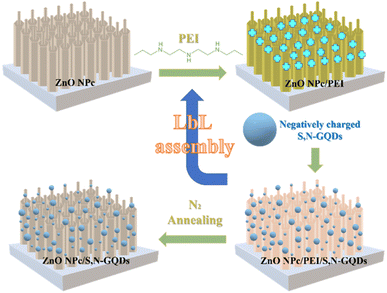 | ||
| Fig. 5 Schematic illustration for manufacturing ZnO NPc/S,N-GQDs heterostructure composites through LbL technique. | ||
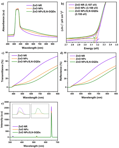
The optical properties of all studied samples were investigated using UV-Vis diffuse reflectance spectra (DRS). As shown in Fig. 6a, a significant absorption peak in the UV area was identified for several samples, which is attributed to the band gap excitation of ZnO. Furthermore, it was discovered that ZnO NPc and ZnO NPc/S,N-GQDs heterostructures composites have a broad and higher absorption peak when compared to blank ZnO NR, particularly in the visible area extending from 400 nm to 800 nm. Notably, the DRS measurement of ZnO NR indicates weak absorption above 400 nm, which fits with its bandgap energy value of 3.187 eV (Fig. 6b). ZnO NPc/S,N-GQDs heterostructures exhibited strong absorption in the same wavelength range, highlighting the importance of SN-GQDs as photo-sensitizers in ZnO NPc/S,N-GQDs heterostructure composite, which has a lower bandgap energy compared to the bare of ZnO NPc.
The transmittance and reflectance spectra in Fig. 6c and d show that when the energy of excitation photons surpasses the ZnO band gap (λ < ∼390 nm), the optical characteristics of the three samples are quite comparable. The most remarkable changes from these three ZnO samples occur in the visible light band (400–800 nm) and may be mainly attributed to scattering between primary and secondary ZnO nanostructures.4 The transmittance at a wavelength of 650 nm through the ZnO NR, ZnO NPc, and ZnO/S,N-GQDs composite are 43.29, 22, and 14.96%, respectively (Fig. 6c). The increase in surface coverage of the corresponding ZnO nanostructures on FTO substrates may result in a decrease in transmittance percent from these three samples. The reflectance of the ZnO NR, ZnO NPc, and ZnO NPc/S,N-GQDs at 650 nm is 43.34, 21.99, and 14.99%, respectively (Fig. 6d). This suggests that as multi-dimensional complexity evolves, more incident light is reflected among the dense secondary branches in a scattering mode.39 Thus, it is reasonable that the sum of transmittance and reflectance of our samples might not reach 100% because the rest of the light is considered to be scattered and absorbed by its sample regarding to a equation (A + S) = 100 − R − T.4 Fig. S4a and b† illustrate how light could be scattered by the complexity of ZnO superstructure. When it comes to ZnO NPc morphology, the multiple reflection effect rises dramatically, increasing light absorption and decreasing light surface reflection. The nanopencil many reflections prolong the light absorption route, allowing additional interaction sites to engage with the light. Subsequently, the energy harvesting of ZnO NPc outweigh the ZnO NR.
The photoluminescence (PL) spectra of three samples excited at a photon energy of 3.81 eV (325 nm) are presented in Fig. 6e. The blue emission peak centered at 320 nm is assigned to the radiative recombination of an electron occupying a shallow donor level and a hole in the top of the valence band.40 The intensity of ZnO NPc and ZnO NPc/S,N-GQDs's blue emission peak, are lower than ZnO NR, indicating that the two samples lack electron recombination. The green emission centered at 523 nm is assigned to the oxygen vacancies (VO),41,42 while the red emission centered at 648 nm is designated to the zinc interstitial defects (Zni).43
Both Zni and VO trap charge carriers, which delays the electron recombination process; however, the inherent nature of VO allows them to reside in both the grain borders (V++O) and the bulk of the grain  . Due to a trapped hole at V++O and a delayed hole at VB, as a result, an electron is delayed at CB and can participate in the photocatalytic activity in addition to the trapped hole at
  . This twofold impact is not seen in zinc interstitial defects (Zni), making them less efficient when compared to VO.44 Surprisingly, ZnO NPc/S,N-GQDs have an oxygen vacancies defect, indicating they are more beneficial for water-splitting applications compared to others.
Analysis of PEC water splitting performance
PEC water splitting performance of the prepared samples was carried out in a three-electrode system. Na2SO4 aqueous solution (0.5 M, pH 7.0) was used as the electrolyte. The effect of ZnO dimension complexity and S,N-GQDs sensitization on ZnO through PEC water splitting performances were studied. Fig. 7a shows the comparison linear sweep voltammogram curves of the bare ZnO as a representative of 1D-ZnO, bare ZnO NPc as a representative of 3D-ZnO, and ZnO NPc/S,N-GQDs under solar simulator illumination (AM 1.5 G, 100 mW cm−2) in a potential window from −0.2 to +1.2 V vs. Ag/AgCl.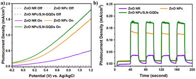 | ||
| Fig. 7 PEC performances (a) photocurrent density vs. applied voltage curves and (b) transient photocurrent responses of three samples with zero bias (0 V) vs. Ag/AgCl collected every 20 seconds. | ||
It was found that a little current density (0.001 mA cm−2) was seen during the scan for the three samples in the dark. However, when illuminated by simulated solar light, the ZnO NPc/S,N-GQDs stood out with a maximum current density of 1.82 mA cm−2 at +1.2 V (vs. Ag/AgCl), representing a 153% and 357% improvement over the ZnO NPc (1.19 mA cm−2) and the ZnO NR (0.51 mA cm−2), respectively. It is in line with the result of photoluminescence characterization (Fig. 6e) where the oxygen vacancy defects lie on ZnO NPc/S,N-GQDs which will enhance its electrical properties and leading to the good water splitting performance. On all three samples, it was notable that no photocurrent density saturation was seen at the maximum recorded potential, i.e., +1.2 V (vs. Ag/AgCl in this research), indicating effective charge separation and collection in these special ZnO nano-architectures under visible light irradiation.
The periodic on/off transient photocurrent responses of several samples to intermittent simulated solar light irradiation are shown in Fig. 7b. Obviously, the consistent decorating of S,N-GQDs significantly enhanced the photocurrent of ZnO NPc. In contrast to bare ZnO NR (1D-ZnO) and ZnO NPc (3D-ZnO), the photocurrent enhancement in the ZnO NPc/S,N-GQDs heterostructure is about six times and one times more (1.3 times), respectively. Under the same experimental settings, ZnO NPc/S,N-GQDs heterostructures outperformed their competitors in terms of photocurrent, suggesting that these heterostructures had the highest photosensitization efficiency for photoexcited electron–hole pairs. A comparative result study based on the PEC performance of similar ZnO/QDs heterostructure composites was listed in Table 1.
| ZnO morphology | Sensitizer | Photocurrent density | Ref. |
|---|---|---|---|
| ZnO nanowires (1D) | N-GQDs | 0.6 mA cm−2 at 1.0 V vs. Ag/AgCl (0.5 Na2SO4) | 29 |
| 3D-ZnO hierarchical nanostructures | C-dots | 0.72 mA cm−2 at 1.23 V vs. RHE (0.5 Na2SO4) | 15 |
| ZnO nanoflake (3D) | CQDs | 0.54 mA cm−2 at 1.23 V vs. RHE (0.5 Na2SO4) | 45 |
| ZnO nanosheets | C-dots | 0.831 mA cm−2 at 0 V vs. Ag/AgCl (0.5 Na2SO4) | 46 |
| ZnO nanopencil (3D) | S,N-GQDs | 1.82 mA cm−2 at 1.2 V vs. Ag/AgCl (0.5 Na2SO4) | Our work |
By putting forth a PEC water splitting mechanism, Fig. 8 shows how significantly PEC performances may be enhanced utilizing the existing ZnO NPc/S,N-GQDs heterostructure. According to the Kohn–Sham molecular orbitals (MOs) theory, numerous electron transitions in S,N-GQDs can be initiated from the occupied levels (i.e., highest occupied molecular orbital, HOMO) to the unoccupied levels (i.e., lowest unoccupied molecular orbital, LUMO) under light irradiation.47,48 Due to the advantageous bandgap of the ZnO NPc/S,N-GQDs heterostructure (3.155 eV), S,N-GQDs in our reaction system may be photoexcited in this manner under simulated sunlight, resulting in the generation of electron–hole pairs.
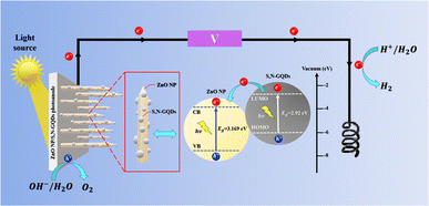 | ||
| Fig. 8 Schematic representation of the PEC water splitting mechanism over the heterostructure of ZnO NPc/S,N-GQDs under sun simulator light irradiation. | ||
Furthermore, since the LUMO potential of S,N-GQDs is more negative than the conduction band (CB) edge of ZnO, and an intimate S,N-GQDs to ZnO NPc interfacial connection developed from the LbL approach, photoexcited electrons created in situ from S,N-GQDs under light irradiation may be spontaneously transported to the CB of ZnO.29 As a result, photogenerated electrons and holes are efficiently separated over S,N-GQDs, and the lifespan of electron–hole charge carriers is greatly extended.
The photocurrent produced by the simultaneous passage of photoelectrons from the LUMO of S,N-GQDs to the CB of ZnO NPc and external circuit finally causes the reduction of water to hydrogen on the counter electrode (Pt wires). Both S,N-GQDs and ZnO NPc may be photoexcited and produce photoelectrons on the LUMO and CB under visible light irradiation (λ > 400 nm) of the ZnO NPc/S,N-GQDs heterostructure. Following that, the electrons move to the CB of ZnO NPc, reduce water to hydrogen, and the hole on the VB of the ZnO NPc or S,N-GQDs oxidize water to oxygen.29
Conclusions
Sensitization of 3D ZnO NPc heterostructure with S,N/GQDs was successfully achieved by a simple LbL technique based on strong electrostatic interaction. The PEC water splitting performance of the ZnO NPc/S,N-GQDs heterostructure composites outperform the bare ZnO NR and ZnO NPc (the photocurrent density of composites 6 times and 1.3 times higher than bare ZnO NR and bare ZnO NPc) because of its optimum energy harvesting and minimum charge recombination. The most probable reaction mechanisms are suggested, and the increased photocatalytic activity can be attributed to two things. First, the highly effective charge separation of electron–hole pairs in composites caused by the presence of oxygen vacancies and zinc interstitial defects. The second one is the lower bandgap energy on ZnO NPc/S,N-GQDs (3.155 eV) absorb more effectively visible light.Author contributions
A. P. S. and R. A. P. conducted the experiment and characterization, prepared the manuscript. A. S. M. and I. reviewed the results. U. P. and I. P. designed the experiments, discussed the results and implications, and proofread the manuscript. All authors commented on and approved the final version of the manuscript.Conflicts of interest
The authors declare that they have no known competing financial interests or personal relationships that could have appeared to influence the work reported in this paper.Acknowledgements
This work was supported by the grant from Internal Research Grant through Riset Percepatan Lektor Kepala Universitas Padjadjaran under contract number 2203/UN6.3.1/PT.00/2022. The authors acknowledge the facilities, scientific and technical support from Advanced Characterization Laboratories Bandung, National Research and Innovation Agency E-Layanan Sains.Notes and references
- I. Dincer and C. Acar, Int. J. Hydrogen Energy, 2015, 40, 11094–11111 CrossRef CAS.
- J. Joy, J. Mathew and S. C. George, Int. J. Hydrogen Energy, 2018, 43, 4804–4817 CrossRef CAS.
- J. Ren, N. M. Musyoka, H. W. Langmi, M. Mathe and S. Liao, Int. J. Hydrogen Energy, 2017, 42, 289–311 CrossRef CAS.
- X. Sun, Q. Li, J. Jiang and Y. Mao, Nanoscale, 2014, 6, 8769–8780 RSC.
- G. Kaur, Divya, V. R. Satsangi, S. Dass and R. Shrivastav, Int. J. Hydrogen Energy, 2020, 45, 21051–21067 CrossRef CAS.
- P. Peerakiatkhajohn, J.-H. Yun, S. Wang and L. Wang, J. Photonics Energy, 2016, 7, 012006–012027 CrossRef.
- U. Pratomo, R. A. Pratama, I. Irkham, A. P. Sulaeman, J. Y. Mulyana and I. Primadona, Nanomaterials, 2023, 13, 1380 CrossRef CAS.
- S. Sohila, R. Rajendran, Z. Yaakob, M. A. M. Teridi and K. Sopian, J. Mater. Sci.: Mater. Electron., 2016, 27, 2846–2851 CrossRef CAS.
- X. Ren, A. Sangle, S. Zhang, S. Yuan, Y. Zhao, L. Shi, R. L. Z. Hoye, S. Cho, D. Li and J. L. MacManus-Driscoll, J. Mater. Chem. A, 2016, 4, 10203–10211 RSC.
- U. Pratomo, R. Adhia, A. Pramudya, G. T. M. Kadja, M. Khalil and I. Primadona, Mater. Lett., 2023, 337, 133932 CrossRef CAS.
- M. A. Desai, A. N. Vyas, G. D. Saratale and S. D. Sartale, Int. J. Hydrogen Energy, 2019, 44, 2091–2127 CrossRef CAS.
- J. Mujtaba, H. Sun, F. Fang, M. Ahmad and J. Zhu, RSC Adv., 2015, 5, 56232–56238 RSC.
- Y. Bao, C. Wang and J.-Z. Ma, Mater. Des., 2016, 101, 7–15 CrossRef CAS.
- A. A. Ibrahim, R. Kumar, A. Umar, S. H. Kim, A. Bumajdad, Z. A. Ansari and S. Baskoutas, Electrochim. Acta, 2016, 222, 463–472 CrossRef CAS.
- J. Kim, S.-A. Hong and J. Yoo, Chem. Eng. J., 2015, 266, 179–188 CrossRef CAS.
- Y. Xia, J. Wang, R. Chen, D. Zhou and L. Xiang, Crystals, 2016, 6, 1–19 CrossRef.
- M. M. Hashemi, A. Nikfarjam, H. Hajghassem and N. Salehifar, J. Phys. Chem. C, 2020, 124, 322–335 CrossRef CAS.
- L. Hu, Y. Ren, H. Yang and Q. Xu, ACS Appl. Mater. Interfaces, 2014, 6, 14644–14652 CrossRef CAS.
- R. Lv, T. Wang, F. Su, P. Zhang, C. Li and J. Gong, Nano Energy, 2014, 7, 143–150 CrossRef CAS.
- S. Kaviya and E. Prasad, RSC Adv., 2016, 6, 33821–33827 RSC.
- N. G. Shimpi, S. Jain, N. Karmakar, A. Shah, D. C. Kothari and S. Mishra, Appl. Surf. Sci., 2016, 390, 17–24 CrossRef CAS.
- T. Wang, R. Lv, P. Zhang, C. Li and J. Gong, Nanoscale, 2015, 7, 77–81 RSC.
- H. Yang, Z. Jin, H. Hu, G. Lu and Y. Bi, Catalysts, 2017, 7, 99–110 CrossRef.
- M. H. M. Facure, R. Schneider, L. A. Mercante and D. S. Correa, Environ. Sci.: Nano, 2020, 7, 3710–3734 RSC.
- H. Wu, J. Ding, D. Yang, J. Li, Y. Shi and Y. Zhou, Ceram. Int., 2020, 46, 17800–17808 CrossRef CAS.
- Z. Zeng, S. Chen, T. T. Y. Tan and F. X. Xiao, Catal. Today, 2018, 315, 171–183 CrossRef CAS.
- Z. Du, S. L. Shen, Z. H. Tang and J. H. Yang, New Carbon Mater., 2021, 36, 449–467 CrossRef CAS.
- B. Wang, G. I. N. Waterhouse and S. Lu, Trends Chem., 2023, 5, 76–87 CrossRef CAS.
- Z. Zeng, F. X. Xiao, X. Gui, R. Wang, B. Liu and T. T. Yang Tan, J. Mater. Chem. A, 2016, 4, 16383–16393 RSC.
- J. J. L. Hmar, T. Majumder, S. Dhar and S. P. Mondal, Thin Solid Films, 2016, 612, 274–283 CrossRef CAS.
- A. Cai, X. Wang, Y. Qi and Z. Ma, Appl. Surf. Sci., 2017, 391, 484–490 CrossRef CAS.
- H. Xie, C. Hou, H. Wang, Q. Zhang and Y. Li, Nanoscale Res. Lett., 2017, 12, 1–8 CrossRef CAS PubMed.
- D. Qu, M. Zheng, P. Du, Y. Zhou, L. Zhang, D. Li, H. Tan, Z. Zhao, Z. Xie and Z. Sun, Nanoscale, 2013, 5, 12272–12277 RSC.
- D. Qu, Z. Sun, M. Zheng, J. Li, Y. Zhang, G. Zhang, H. Zhao, X. Liu and Z. Xie, Adv. Opt. Mater., 2015, 3, 360–367 CrossRef CAS.
- R. Kumar and S. K. Mishra, Applied Surface Science Advances, 2022, 9, 100256 CrossRef.
- T. Majumder and S. P. Mondal, J. Electroanal. Chem., 2016, 769, 48–52 CrossRef CAS.
- B. Subash, B. Krishnakumar, M. Swaminathan and M. Shanthi, Langmuir, 2013, 29, 939–949 CrossRef CAS PubMed.
- S. Sahu, B. Behera, T. K. Maiti and S. Mohapatra, Chem. Commun., 2012, 48, 8835–8837 RSC.
- J. Kong, Y. Wei, L. Yang, W. A. Yee, Y. Dong, R. Zhou, S. Y. Wong, L. Ke, X. W. Sun, H. Du, X. Li and X. Lu, J. Phys. Chem. C, 2013, 117, 10106–10113 CrossRef CAS.
- S. Ben Ameur, H. BelHadjltaief, B. Duponchel, G. Leroy, M. Amlouk, H. Guermazi and S. Guermazi, Heliyon, 2019, 5, e01912 CrossRef CAS PubMed.
- B. Wang, Z. Wei, L. Sui, J. Yu, B. Zhang, X. Wang, S. Feng, H. Song, X. Yong, Y. Tian, B. Yang and S. Lu, Light: Sci. Appl., 2022, 11(2022), 172 CrossRef CAS.
- X. Yang, X. Li, B. Wang, L. Ai, G. Li, B. Yang and S. Lu, Chin. Chem. Lett., 2022, 33, 613–625 CrossRef CAS.
- S. D. Kshirsagar, U. Pasha Shaik, M. G. Krishna and S. P. Tewari, J. Lumin., 2013, 136, 26–31 CrossRef CAS.
- F. Kayaci, S. Vempati, I. Donmez, N. Biyikli and T. Uyar, Nanoscale, 2014, 6, 10224–10234 RSC.
- C. Liu, Y. Qiu, F. Wang, L. Li, Q. Liang and Z. Chen, Ceram. Int., 2017, 43, 5329–5333 CrossRef CAS.
- C. Mahala, M. D. Sharma and M. Basu, ACS Appl. Nano Mater., 2020, 3, 1999–2007 CrossRef CAS.
- T. F. Yeh, C. Y. Teng, S. J. Chen and H. Teng, Adv. Mater., 2014, 26, 3297–3303 CrossRef CAS PubMed.
- L. Tang, R. Ji, X. Li, K. S. Teng and S. P. Lau, J. Mater. Chem. C, 2013, 1, 4908–4915 RSC.
Footnote |
| † Electronic supplementary information (ESI) available. See DOI: https://doi.org/10.1039/d3ra02907g |
| This journal is © The Royal Society of Chemistry 2023 |

