DOI:
10.1039/D3RA04169G
(Paper)
RSC Adv., 2023,
13, 33634-33643
First-principles study of indium nitride monolayers doped with alkaline earth metals†
Received
21st June 2023
, Accepted 4th November 2023
First published on 16th November 2023
Abstract
Element doping has been widely employed to modify the ground state properties of two-dimensional (2D) materials. In this work, the effects of doping with alkaline earth metals (AEMs) on the structural, electronic, and magnetic properties of indium nitride (InN) monolayers are investigated using first-principles calculations based on density functional theory. In a graphene-like honeycomb structure, the InN monolayer possesses good dynamical and thermal stability, and exhibits an indirect gap semiconductor character with a band gap of 0.37 (1.48) eV as determined by using the PBE(HSE06) functional. A single In vacancy leads to the emergence of a magnetic semiconductor character, where magnetic properties with a large total magnetic moment of 3.00 μB are produced mainly by the N atoms closest to the defect site. The incorporation of AEMs impurities causes local structural distortion due to the difference in atomic size, where Mg and Ca doping processes are energetically most favorable. Half-metallicity is induced by the partial occupancy of the N-2p orbital, which is a consequence of having one valence electron less. In these cases, the total magnetic moment of 1.00 μB mainly originates from N atoms neighboring the dopants. Further increasing the doping level preserves the half-metallic character, where N atoms play a key role on the magnetism of the highly doped systems. Results presented herein suggest the In replacement by AEMs impurities is an effective approach to make prospective spintronic 2D materials from InN monolayers.
1. Introduction
So far, two-dimensional (2D) materials have been widely applied in electronics and optoelectronics,1,2 gas sensing,3–7 energy storage,8,9 catalysis,10,11 and spintronics,12,13 among others, because of their intriguing physical, chemical, and mechanical properties generated from the thickness effects. Amongst them, graphene is a symbolic representative.14,15 However, its zero gap character may restrict its practical applications in many cases. Therefore, opening the graphene band gap and searching for new alternative atom-thickness materials have been simultaneously investigated by researchers. Significant energy gaps have been obtained in graphene by either cutting its edges to form nanoribbons16,17 or by means of chemical surface functionalization.18,19 Additionally, it would be flawed not to mention boron nitride (BN) amongst 2D materials beyond graphene.20 Due to its graphite-like hexagonal bulk phase, BN monolayer can be obtained by an exfoliation-based top-down method,21,22 but also it has been grown by bottom-up methods.23,24 Wickramaratne et al.25 have demonstrated that the insulator character is preserved upon reducing BN thickness, where the band gap decreases about 0.5 eV from the bulk to the monolayer counterpart. The discovery of BN monolayers has aroused interest in 2D graphene-like IIIA-nitrides such as aluminum nitride (AlN), gallium nitride (GaN), and indium nitride (InN) due to their semiconducting properties with relatively large band gaps that decrease according to increases in the atomic number of the IIIA-group atom.26,27
InN is an important material for high-efficiency solar cells28,29 and high-speed electronic devices30,31 due to its narrow band gap (0.7 eV) and high absorbance, and high-speed data transfer. Since the successful fabrication of BN monolayers, the interest in 2D InN materials has been continuously increased, as research results may provide great opportunities to develop new 2D materials. The growth of 2D InN films has been successfully realized by some groups.32,33 Meantime, the monolayer counterpart has been predicted by Şahin et al.34 Results indicate good stability of the planar honeycomb structure and an indirect gap semiconductor nature. Further investigations have shown its good optical absorption in visible and ultraviolet regions.26,35 In addition, different approaches have been also explored to modify the InN monolayer properties in order to get multifunctional 2D materials. For example, Lin et al.36 have investigated the effects of transition metals (Cr, Fe, and Ni) doping on electronic and magnetic properties of InN monolayers. Results indicate significant magnetism induced by doping, where magnetic semiconductor and half-metallic characteristics are obtained by doping with Cr(Fe) and Ni, respectively, to get prospective 2D materials for spintronic applications. Similarly, feature-rich electronic and magnetic properties with a total magnetic moment of 2.00 μB are also obtained by doping with Cu.37 d0 magnetism appears also in InN monolayers through Be and C doping at N sites with magnetic moments of 0.91 and 1.09 μB,38 respectively.
Recently, spintronics or spin-based electronics has been replacing rapidly conventional electronics due to its great advantages such as high-speed processing of a large volume data and low energy consumption.39,40 In this regard, a large variety of materials have been explored for spintronic applications, where d0 spintronic materials (those which contain no magnetic element) have emerged as promising candidates.41,42 In this work, our main aim is to develop new 2D d0 spintronic materials from InN monolayers using a doping approach. Usually, the magnetic properties are produced by hole doping that leads to the partial occupancy of the outermost orbitals, that is the asymmetric charge distribution between their spin channels.43–45 Herein, alkaline earth (Be, Mg, Ca, Sr, and Ba) atoms are selected as impurities, recalling that alkaline earth metals have one valence electron less than In atoms (s2 in comparison with s2p1 valence electronic configuration), such that one can expect significant magnetism in the doped systems induced by one hole. It is anticipated that the pristine monolayer is a non magnetic 2D material, which is significantly magnetized by doping with alkaline earth metals. Consequently, half-metallicity with a total magnetic moment of 1.00 μB is induced. Results suggest the doping is an efficient approach to make new 2D spintronic materials from InN monolayers, an application that is not noted for the pristine monolayer. The paper is organized as follows: Section 2 gives computational parameters that are employed in this work; results are presented and discussed in Section 3, where the structural distortion, spin-polarized electronic band structure and density of states are analyzed. The interactions between dopants and the host monolayer are examined by charge density difference and Bader charge analysis. Magnetism is studied through the total magnetic moments and spin density; finally, the remarkable findings are summarized in Section 4.
2. Computational details
Based on Density Functional Theory (DFT),46 the Projector Augmented Wave (PAW) implemented in the Vienna Ab initio Simulation Package (VASP)47,48 is employed to perform first-principles calculations. Electron exchange–correlation interactions are determined by the Generalized Gradient Approximation of Perdew–Burke–Ernzerhof (GGA-PBE),49 while more accurate calculations of the electronic band gap are reached by the hybrid functional HSE06.50 The cutoff energy of the plane wave is set to 500 eV. An energy tolerance of 10−6 eV is employed for the self-consistent convergence. The structures are relaxed with a maximum residual force of 0.01 eV Å−1. In addition, the Brillouin zones are sampled by a 4 × 4 × 1 Monkhorst–Pack k-point mesh.51 To minimize the interactions between periodic layers, a vacuum gap of 14.5 Å is inserted in the direction perpendicular to the monolayer plane.
The effects of single In vacancy and doping are investigated using a 4 × 4 × 1 supercell containing 32 atoms (16 In atoms and 16 N atoms). In the first case, one In atom is removed to get a vacancy concentration of 6.25%. A doping level of 6.26% is also modeled by replacing one In atom by one alkaline earth metal. The formation energy Ef is determined as follows:
| | |
Ef = Et − Em(InN) + μIn − μD
| (1) |
where
Et and
Em(InN) denote the total energy of the doped and pristine InN monolayer, respectively;
μIn and
μD are chemical potential of In and the dopant atom, respectively. Then, the chemical stability will be examined through the cohesive energy
Ec, which is calculated using following expression:
| |
 | (2) |
herein,
ni is number of atom “
i” in the system, while the energy of an isolated “
i” atom is denoted by
E(
i). From the equation, negative
Ec values may suggest good chemical stability of the systems, where the compound state is energetically more favorable than the decomposed state, and
vice versa.
3. Results and discussion
3.1. Stability and electronic properties of InN monolayers
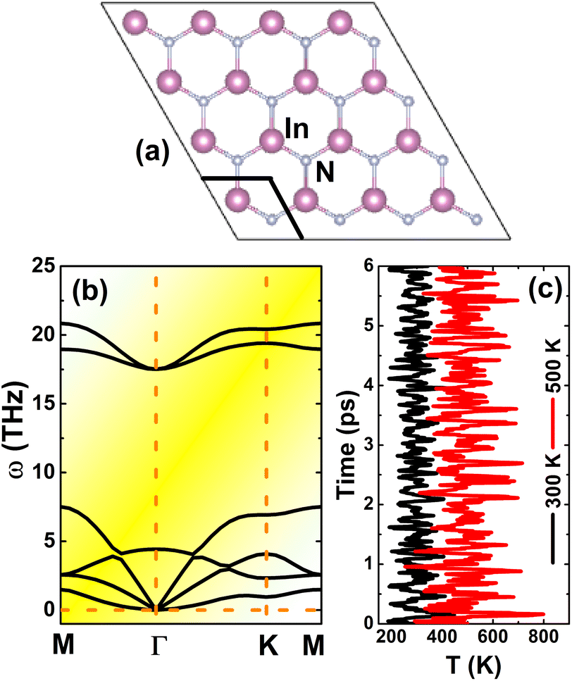
Similar to other IIIA-nitride monolayers, InN monolayers adopt the graphene-like planar honeycomb structure (space group P![[6 with combining macron]](https://www.rsc.org/images/entities/char_0036_0304.gif) m2 – no. 187),34,52 in which In and N atoms are alternated. Fig. 1a shows a 4 × 4 × 1 supercell, where a unit cell containing two inequivalent atoms (one In atom and one N atom) is clearly indicated. The equilibrium structure is characterized by a lattice constant of 3.64 Å and chemical bond length of 2.10 Å, which are in good agreement with previous calculations.53,54 Further examination of the stability is based on the phonon dispersion curve and Ab Initio Molecular Dynamics (AIMD). From Fig. 1b, one can conclude that the InN monolayer is dynamically stable since no soft phonon mode is observed in the phonon spectra. In addition, the thermal stability is also confirmed by AIMD simulations as displayed in Fig. 1c; results suggest temperature-induced atomic vibrations around equilibrium positions without any broken chemical bond.
m2 – no. 187),34,52 in which In and N atoms are alternated. Fig. 1a shows a 4 × 4 × 1 supercell, where a unit cell containing two inequivalent atoms (one In atom and one N atom) is clearly indicated. The equilibrium structure is characterized by a lattice constant of 3.64 Å and chemical bond length of 2.10 Å, which are in good agreement with previous calculations.53,54 Further examination of the stability is based on the phonon dispersion curve and Ab Initio Molecular Dynamics (AIMD). From Fig. 1b, one can conclude that the InN monolayer is dynamically stable since no soft phonon mode is observed in the phonon spectra. In addition, the thermal stability is also confirmed by AIMD simulations as displayed in Fig. 1c; results suggest temperature-induced atomic vibrations around equilibrium positions without any broken chemical bond.
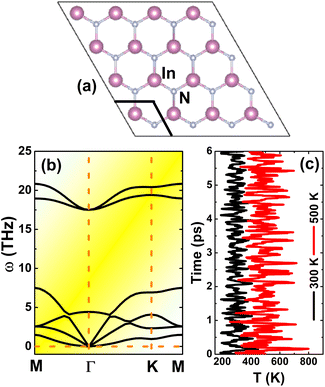 |
| | Fig. 1 (a) A 4 × 4 × 1 supercell (an unit cell is marked), (b) phonon dispersion curves, and (c) AIMD simulation at 300 and 500 K of InN monolayer (see Fig. S1† for the fluctuation of energy). | |
Once the InN monolayer stability is confirmed, its electronic properties are investigated. The electronic band structure displayed in Fig. 2a indicates the indirect-gap semiconductor character of the InN monolayer, considering the valence band maximum and conduction band minimum at the K and Γ points, respectively. Similar profiles are obtained by PBE and HSE06 functionals, however they provide energy gaps of 0.37 and 1.48 eV, respectively. Results satisfy the expectation of the larger HSE06 band gap since standard GGA-PBE underestimates usually the material’s band gap. The forbidden energy range is also observed in the total density of states (TDOS) spectra given in Fig. S2 of the ESI file.† From Fig. 2b, one can see that N-pz contributes mainly to the upper part of the valence band, meanwhile the lower part is formed mainly by the In-s state. This latter state also originates the lower part of the conduction band. Projected density of states (PDOS) features suggest the charge transfer from In-5s and In-5p orbitals (to be unoccupied) to the N-3p orbital (to be filled). To fully describe the transfer process, the valence charge distribution is calculated, which asserts the charge enrichment at N sites (illustrated in Fig. 2c). In addition, the Bader charge analysis confirms that the N atom receives a charge amount of 1.23 e from the In atom, that is the charge is transferred from the less to more electronegative atom.
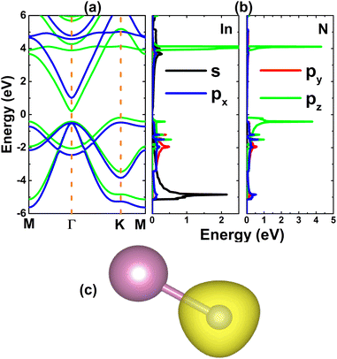 |
| | Fig. 2 (a) Electronic band structure calculated with PBE (green curve) and HSE06 (blue curve) functionals, (b) projected density of states, and (c) charge distribution (iso-surface value: 0.08 e Å−3) of the InN monolayer. | |
3.2. Effects of a single In vacancy
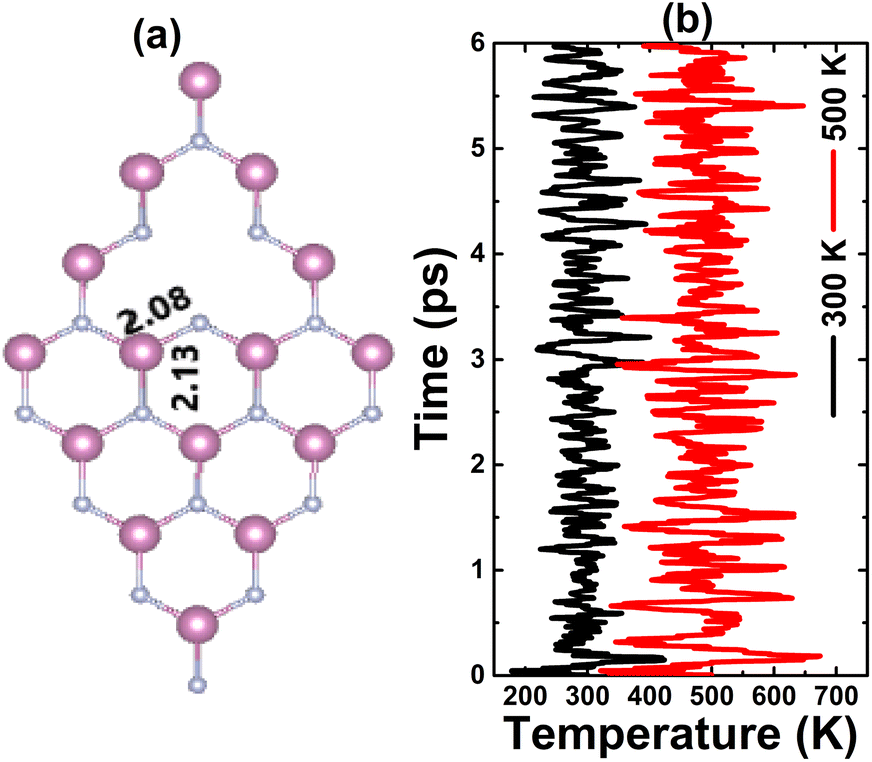
Fig. 3a shows the relaxed atomic structure of an InN monolayer with a single In vacancy. A slight structural contraction can be noted caused by a defect, which is reflected in a slight decrease of the first chemical bond length from the vacancy site. Our calculations yield a formation energy value of 6.09 eV. Further AIMD simulations indicate no structural destruction (see Fig. 3b) at 300 and 500 K, such that the monolayer maintains its integrity after creating a single In vacancy. Moreover, a negative Ec value of −3.00 eV per atom suggest also the chemical stability of the vacancy-defected system. It is important to mention that this value is slightly less negative than that of the pristine monolayer (−3.17 eV per atom), indicating a slight reduction of chemical stability caused by single In vacancy.
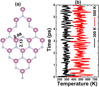 |
| | Fig. 3 (a) Optimized atomic structure and (b) AIMD simulations at 300 and 500 K of an InN monolayer with a single In vacancy (see Fig. S3† for the fluctuation of the energy). | |
Fig. 4 shows the spin-polarized band structure of the defective system, which asserts the magnetic semiconductor nature. The spin polarization is observed mainly around the Fermi level, the energy gaps of the spin-up and spin-down state are 0.65 and 0.26 eV, respectively. The smaller spin-down band gap is a result of new middle-gap energy states appearing mostly in the spin-down channel. The band structure profiles are in good agreement with the TDOS spectra displayed in Fig. S4 of the ESI file;† both suggest significant magnetization of the InN monolayer by creating a single In vacancy, which is reflected in a total magnetic moment of 3 μB. The spin density illustrated in Fig. 5a indicates N atoms closest to the defect site as mainly responsible for the magnetization, which exhibit the unbalanced charge distribution between spin channels. To investigate in more detail the origin of the magnetism, PDOS spectra of these magnetic atoms are given in Fig. 5b. Note that the magnetism originates mainly from the N-p orbital, where flat energy curves in the vicinity of the Fermi level are formed by N-px,y and N-pz states. These results are reasonable since the creation of a single In vacancy leads to a deficit of charge in the N-2p orbital demonstrated by a Bader charge of −0.84 e, that is, first N neighbor atoms around the vacancy site receive a smaller charge quantity in comparison with those in the perfect monolayer (−1.23 e). Consequently, the N-2p orbital is only partially occupied to gain magnetic properties.
 |
| | Fig. 4 Spin-polarized band structure (the Fermi level is set to 0 eV; black curve: spin-up; red curve: spin-down) of the InN monolayer with a single In vacancy. | |
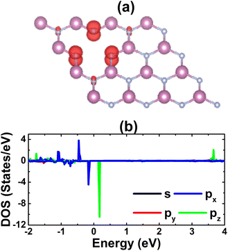 |
| | Fig. 5 (a) Spin density (iso-surface value: 0.01 e Å−3) and (b) projected density of states of N atoms closest to the vacancy site in the InN monolayer with a single In vacancy. | |
3.3. Effects of doping with alkaline earth metals
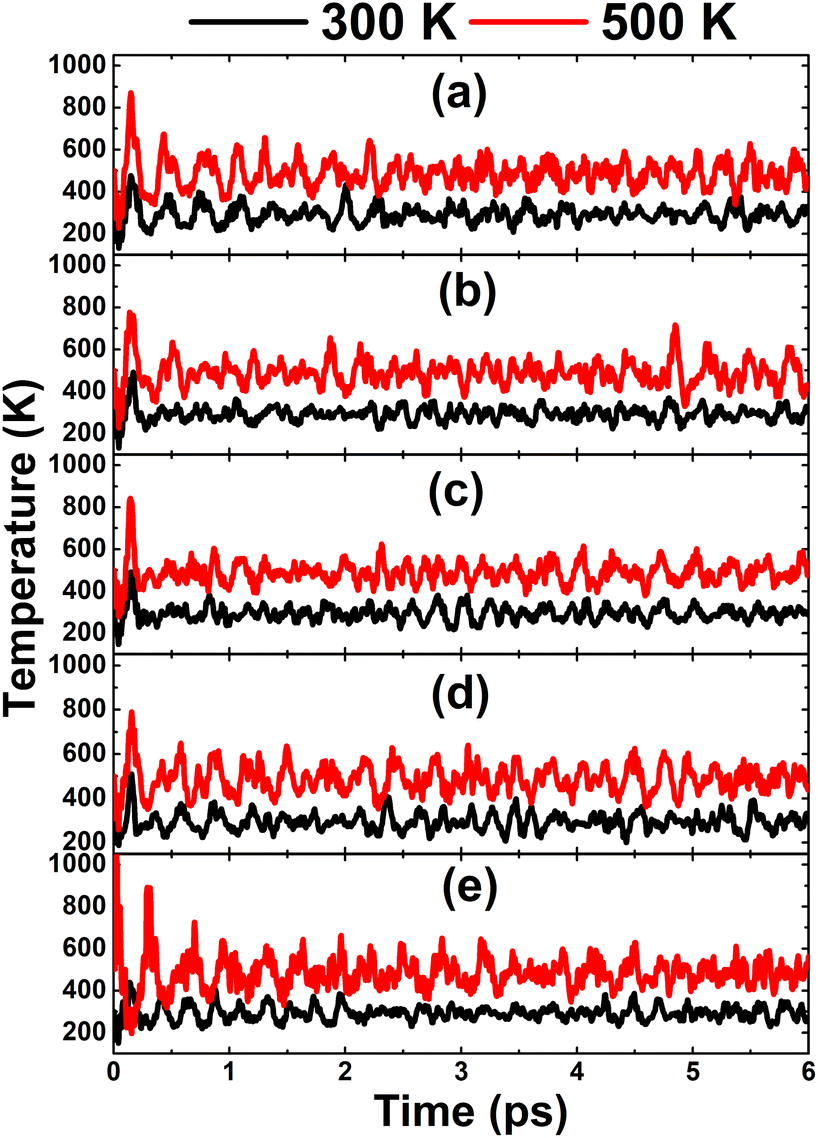
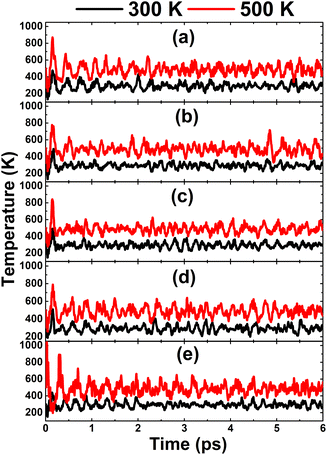
In this part, the effects of alkaline earth metals impurities in the InN monolayer are analyzed. Fig. 6 shows the relaxed chemical bond length around the doping site. Note that the atomic distance from dopants to their closest N atoms increases according to the increase in its atomic number. Consequently, the chemical bond length dN–In decreases slightly. Be and Mg doping causes a local contraction, meanwhile a structural tension is observed in the cases of doping with Ca, Sr, and Ba. These structural features follow the size criterion considering the In atomic radius of 1.55 Å; this value is larger than that of Be (1.05 Å) and Mg (1.50 Å), and smaller than that of Ca (1.80 Å), Sr (2.00), and Ba (2.15 Å).55 The obtained results from our calculations for the doped systems are summarized in Table 1. Applying eqn (1), doping energies of −0.11, −0.35, −0.39, 0.28, 0.81 eV are obtained for replacing the In atom by Be, Mg, Ca, Sr, and Ba impurities, respectively. These results suggest an exothermic process of doping with the first three metals, meanwhile doping with Sr and Ba may be energetically less favorable and require supplying additional energy. Once the impurities are incorporated, the doped systems exhibit good thermal stability at room temperature as indicated by the AIMD simulations in Fig. 7. To be precise, the monolayer structural integrity is maintained at 300 and 500 K under the doping process, where impurities cause no chemical bond breaking. Further, the good chemical stability of Be-, Mg-, Ca-, Sr-, and Ba-doped InN monolayers is also suggested by negative Ec values of −3.22, −3.16, −3.17, −3.14, and −3.13 eV per atom, respectively. Note that these values exhibit quite a small difference in comparison with that of pristine monolayer, indicating that doping process affects insignificantly the chemical stability of the InN monolayer.
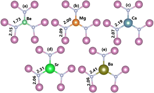 |
| | Fig. 6 Chemical bond lengths around the doping site of an InN monolayer doped with (a) Be, (b) Mg, (c) Ca, (d) Sr, and (e) Ba. | |
Table 1 Formation energy Ef (eV), cohesive energy Ec (eV per atom), electronic band gap Eg (eV; spin-up/spin-down, M: metallic), charge transferred from impurity ΔQ (e), and total magnetic moment Mt (μB) of an InN monolayer doped with alkaline earth metals
| |
Ef |
Ec |
Eg |
ΔQ |
Mt |
| Be-doped |
−0.11 |
−3.22 |
0.44/M |
1.66 |
1.00 |
| Mg-doped |
−0.35 |
−3.16 |
0.60/M |
1.59 |
1.00 |
| Ca-doped |
−0.39 |
−3.17 |
0.72/M |
1.47 |
1.00 |
| Sr-doped |
0.28 |
−3.14 |
0.63/M |
1.49 |
1.00 |
| Ba-doped |
0.81 |
−3.13 |
0.58/M |
1.46 |
1.00 |
 |
| | Fig. 7 AIMD simulations at 300 and 500 K of an InN monolayer doped with (a) Be, (b) Mg, (c) Ca, (d) Sr, and (e) Ba (see Fig. S5† for the fluctuation of energy). | |
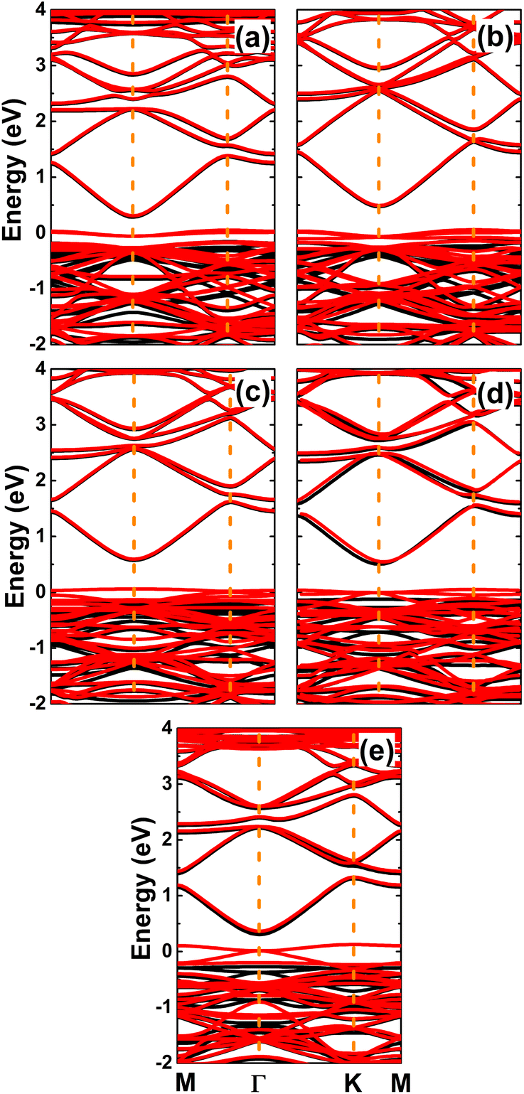
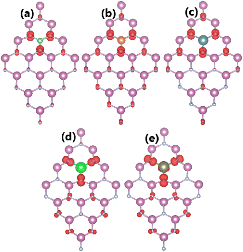
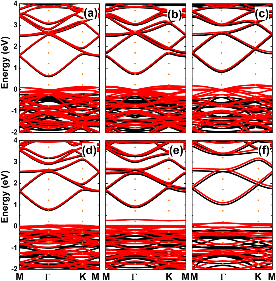
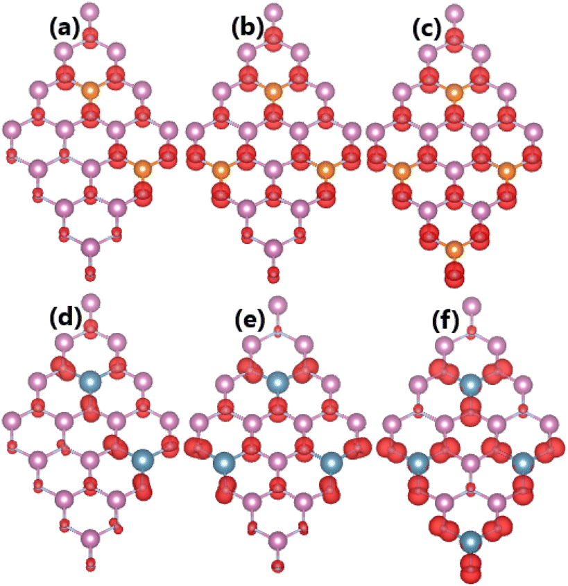
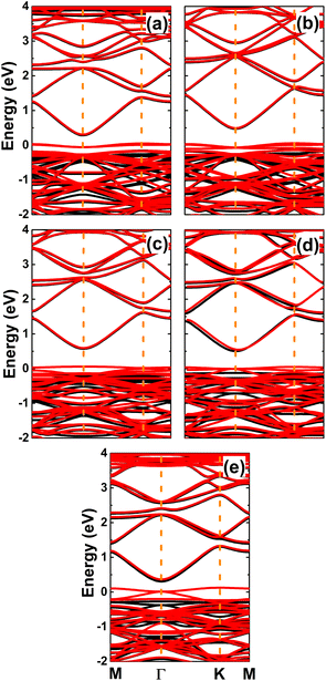
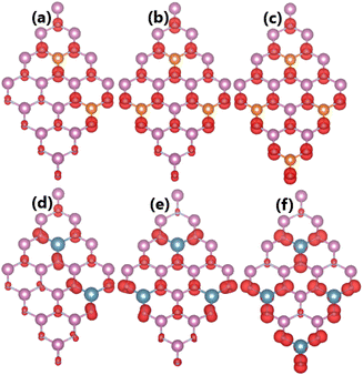
The spin-polarized band structures of an InN monolayer doped with alkaline earth metals are displayed in Fig. 8. It can be noted from the spin polarization that mostly the upper part of the valence band is in the vicinity of the Fermi level. New middle-gap energy states overlap with the Fermi level in the spin-down channel. Meanwhile, the semiconductor character is preserved in the spin-up channel with band gaps of 0.44, 0.60, 0.72, 0.63, and 0.58 eV for the Be-, Mg-, Ca-, Sr-, and Ba-doped InN monolayers, respectively. The band structure profiles indicate half-metallicity with perfect 100% spin polarization around the Fermi level, which is a desirable feature to generate spin current.56,57 This feature-rich electronic property is also confirmed by the TDOS spectra in Fig. S6 of the ESI file.† Undoubtedly the changes in electronic interactions around the doping site are responsible for the new electronic features. Fig. 9 shows the charge density difference, which is calculated as follows: Δρ = ρ(m + D) − ρ(m) − ρ(D), where the terms in right hand side denote the charge density of the doped system, the InN monolayer, and separated dopant atom, respectively. From the figure, one can see significant charge depletion at doping sites, meanwhile charge enrichment is observed at their neighboring sites. Therefore, it can be concluded that alkaline earth metals act as charge donors transferring charge to the host monolayer. Further Bader charge analysis indicates a charge transfer of 1.66, 1.59, 1.47, 1.49, and 1.46 e from Be, Mg, Ca, Sr, and Ba impurities, respectively.
 |
| | Fig. 8 Spin-polarized band structures (the Fermi level is set to 0 eV; black curve: spin-up; red curve: spin-down) of InN monolayers doped with (a) Be, (b) Mg, (c) Ca, (d) Sr, and (e) Ba. | |
 |
| | Fig. 9 Charge density differences (Iso-surface value: 0.002 e Å−3; aqua surface: charge depletion; yellow surface: charge accumulation) in InN monolayers doped with (a) Be, (b) Mg, (c) Ca, (d) Sr, and (e) Ba. | |
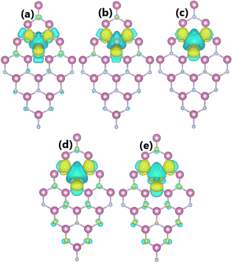
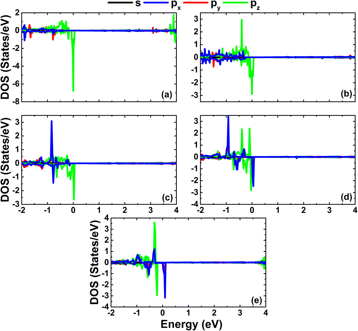
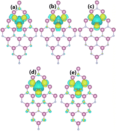
As expected, alkaline earth impurities have induced significant magnetism in the InN monolayer, which is confirmed by the spin-asymmetric band structures as analyzed above and a total magnetic moment of 1 μB. Further investigation of the origin of the magnetism is based on the spin density illustrated in Fig. 10. Note that the first neighbor N atoms of impurities mainly produce the magnetic properties. Recall that in the pristine monolayer, the N-2p orbital is fully occupied due to the charge transfer from In atoms. However, when substituting one In atom by one impurity with one valence electron less, the charge transfer from impurities to N atoms is not enough to fulfil the N-2p orbital. Consequently, this orbital is the main contributor to the magnetism. This feature is demonstrated by means of the PDOS spectra in Fig. 11, which indicate clearly the spin asymmetry of px, py, and pz states, where the presence of the N-2s state is negligible.
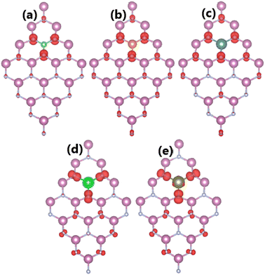 |
| | Fig. 10 Spin densities (iso-surface value: 0.004 e Å−3) in InN monolayers doped with (a) Be, (b) Mg, (c) Ca, (d) Sr, and (e) Ba. | |
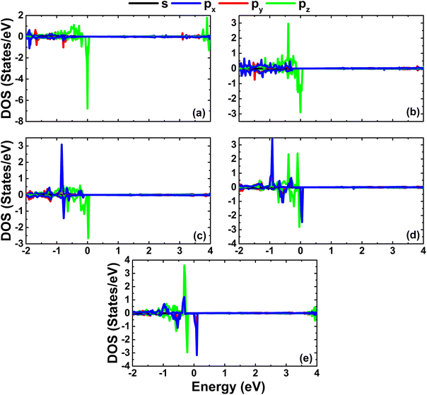 |
| | Fig. 11 Projected densities of N atoms close to the doping site in InN monolayers doped with (a) Be, (b) Mg, (c) Ca, (d) Sr, and (e) Ba. | |
3.4. Effects of doping level
Since Mg and Ca doping processes are energetically most favorable, we further investigate the effects of doping level by increasing this to 12.5%, 18.75%, and 25%. The calculated spin-polarized band structures (see Fig. 12) indicate a half-metallic character regardless dopant concentration. However, the spin-up band gap increases according to increases in the doping level. Specifically, energy gaps of 0.82, 1.03, 1.18 eV are obtained by doping with 12.5%, 18.75%, and 25% of Mg. In the same pattern, the semiconductor spin channel has band gaps of 0.97, 1.03, and 1.19 eV, respectively, by doping with Ca.
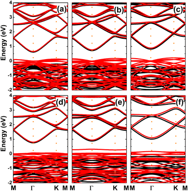 |
| | Fig. 12 Spin-polarized band structures (the Fermi level is set to 0 eV; black curve: spin-up; red curve: spin-down) of InN monolayers doped with (a) 12.5%, (b) 18.75%, (c) 25% of Mg; and (d) 12.5%, (e) 18.75%, and (f) 25% of Ca. | |
Our calculations show that the magnetization becomes stronger when increasing the doping level. Specifically, total magnetic moments of 2.00, 3.00, and 4.00 μB are obtained by doping with 12.5%, 18.75%, and 25% of both Mg and Ca impurities. Fig. 13 illustrates the spin density in the highly doped systems. The results indicate the key role of N atoms around doping sites in originating magnetism. Far away from the impurities, the contribution becomes smaller due to the less affected electronic interactions.
 |
| | Fig. 13 Spin densities (iso-surface value: 0.004 e Å−3) in InN monolayers doped with (a) 12.5%, (b) 18.75%, (c) 25% of Mg; and (d) 12.5%, (e) 18.75%, and (f) 25% of Ca. | |
Finally, the thermal stability is examined by AIMD simulations in Fig. 14. The results imply that the highly doped systems are thermally stable at room temperature and a high temperature of 500 K. Once the chemical bonds are formed, they can be stabilized without any decomposition into separated atoms. It is important to mention the aggregation phenomenon of impurities in highly doped systems.58,59 However, with the confirmed thermal stability and deeply negative cohesive energy of between −3.16 and −3.11 eV per atom, it is believed that the scattered impurity distribution in InN monolayers has good stability. This feature also originates from the large difference in electronegativity between alkaline earth metals and their neighbor N atoms, which favors the formation of stable ionic chemical bonds through the charge transfer process.
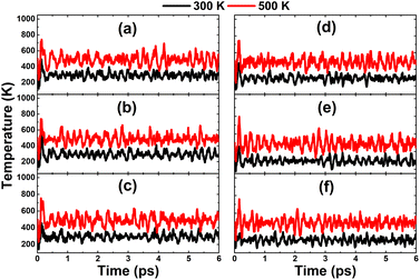 |
| | Fig. 14 AIMD simulations at 300 and 500 K of InN monolayers doped with (a) 12.5%, (b) 18.75%, (c) 25% of Mg; and (d) 12.5%, (e) 18.75%, and (f) 25% of Ca (see Fig. S7† for the fluctuation of energy). | |
4. Conclusions
In summary, a systematic first-principles study has been carried out to explore the effects of alkaline earth impurities (Be, Mg, Ca, Sr, and Ba) on the structural, electronic, and magnetic properties of InN monolayers. The InN monolayer is an indirect gap 2D material, whose band gap is formed by the separation between the N-2pz state in the upper part of the valence band and the In-5s state in the lower part of the conduction band. The valence charge distribution and Bader charge analysis indicate a charge transfer of 1.23 e from the In atom to the N atom to generate the ionic chemical bonds. The presence of an In single vacancy causes a slight structural contraction, while AEM dopants induce either structural contraction or tension depending on the difference in atomic size. Be, Mg, and Ca doping processes are thermodynamically exothermic with negative doping energies, while endothermic processes characterize the remaining cases. The magnetic semiconductor behavior is induced by creating an In single vacancy with spin-up/spin-down band gaps of 0.65/0.26 eV and a total magnetic moment of 3.00 μB, while AEM impurities lead to the appearance of a half-metallic character with total magnetic properties of 1.00 μB and semiconductor spin energy gaps of 0.44, 0.60, 0.72, 0.63, and 0.58 for the Be-, Mg-, Ca-, Sr-, and Ba-doped systems, respectively. In all cases, the electronic and magnetic properties are mainly regulated by the 2p orbital of N atoms closest to the defect-doping site, where the partial occupancy makes an unbalanced charge distribution between spin channels. Further investigations demonstrate the preservation of the half-metallicity regardless of the doping level up to 25%. In addition, all the defective and doped systems exhibit good thermal stability, that is they can be stable upon increasing the temperature to 300 and 500 K after formation. The presented results may pave a solid way to make the InN monolayer a prospective spintronic material, which is not considered for the pristine counterpart due to the absence of magnetism.
Computational resources
Calculations were performed in the DGCTIC-UNAM Supercomputing Center (projects LANCAD-UNAM-DGTIC-368).
Data availability
The data that support the findings of this study are available from the corresponding author upon request.
Conflicts of interest
The authors declare that they have no known competing financial interests or personal relationships that could have appeared to influence the work reported in this paper.
Acknowledgements
This research is funded by Thai Nguyen University of Education under Project number TNUE-2022-09. D. M. Hoat expresses his gratitude to all the valuable support from Duy Tan University, who is going to celebrate its 30th anniversary of establishment (Nov. 11, 1994 – Nov. 11, 2024) towards “Integral, Sustainable and Stable Development”.
References
- J. Shim, H.-Y. Park, D.-H. Kang, J.-O. Kim, S.-H. Jo, Y. Park and J.-H. Park, Electronic and optoelectronic devices based on two-dimensional materials: From fabrication to application, Adv. Electron. Mater., 2017, 3(4), 1600364 CrossRef.
- Q. A. Vu and W. J. Yu, Electronics and optoelectronics based on two-dimensional materials, J. Korean Phys. Soc., 2018, 73, 1–15 CrossRef.
- B. Wang, Y. Gu, L. Chen, L. Ji, H. Zhu and Q. Sun, Gas sensing devices based on two-dimensional materials: A review, Nanotechnology, 2022, 33(25), 252001 CrossRef PubMed.
- S. S. Varghese, S. H. Varghese, S. Swaminathan, K. K. Singh and V. Mittal, Two-dimensional materials for sensing: graphene and beyond, Electronics, 2015, 4(3), 651–687 CrossRef CAS.
- S. Zhai, X. Jiang, D. Wu, L. Chen, Y. Su, H. Cui and F. Wu, Single Rh atom decorated pristine and S-defected PdS2 monolayer for sensing thermal runaway gases in a lithium-ion battery: A first-principles study, Surf. Interfaces, 2023, 37, 102735 CrossRef CAS.
- H. Wu, Y. Xia, C. Zhang, S. Xie, S. Wu and H. Cui, Adsorptions of C5F10O decomposed compounds on the Cu-decorated NiS2 monolayer: a first-principles theory, Mol. Phys., 2023, 121(3), e2163715 CrossRef.
- Z. Nie, C. Wang, R. Xue, G. Xie and H. Xiong, Two-dimensional FePc and MnPc monolayers as promising materials for SF6 decomposition gases detection: Insights from DFT calculations, Appl. Surf. Sci., 2023, 608, 155119 CrossRef CAS.
- H. Tao, Q. Fan, T. Ma, S. Liu, H. Gysling, J. Texter, F. Guo and Z. Sun, Two-dimensional materials for energy conversion and storage, Prog. Mater. Sci., 2020, 111, 100637 CrossRef CAS.
- B. Mendoza-Sánchez and Y. Gogotsi, Synthesis of two-dimensional materials for capacitive energy storage, Adv. Mater., 2016, 28(29), 6104–6135 CrossRef PubMed.
- D. Deng, K. Novoselov, Q. Fu, N. Zheng, Z. Tian and X. Bao, Catalysis with two-dimensional materials and their heterostructures, Nat. Nanotechnol., 2016, 11(3), 218–230 CrossRef CAS PubMed.
- J. Di, C. Yan, A. D. Handoko, Z. W. Seh, H. Li and Z. Liu, Ultrathin two-dimensional materials for photo-and electrocatalytic hydrogen evolution, Mater. Today, 2018, 21(7), 749–770 CrossRef CAS.
- A. Avsar, H. Ochoa, F. Guinea, B. Özyilmaz, B. Van Wees and I. J. Vera-Marun, Colloquium: Spintronics in graphene and other two-dimensional materials, Rev. Mod. Phys., 2020, 92(2), 021003 CrossRef CAS.
- N. Sethulakshmi, A. Mishra, P. M. Ajayan, Y. Kawazoe, A. K. Roy, A. K. Singh and C. S. Tiwary, Magnetism in two-dimensional materials beyond graphene, Mater. Today, 2019, 27, 107–122 CrossRef CAS.
- S. Bharech and R. Kumar, A review on the properties and applications of graphene, J. Mater. Sci. Mech. Eng., 2015, 2(2025), 70–73 Search PubMed.
- S. Ren, P. Rong and Q. Yu, Preparations, properties and applications of graphene in functional devices: A concise review, Ceram. Int., 2018, 44(11), 11940–11955 CrossRef CAS.
- Y.-W. Son, M. L. Cohen and S. G. Louie, Energy gaps in graphene nanoribbons, Phys. Rev. Lett., 2006, 97(21), 216803 CrossRef PubMed.
- Y.-C. Chen, D. G. De Oteyza, Z. Pedramrazi, C. Chen, F. R. Fischer and M. F. Crommie, Tuning the band gap of graphene nanoribbonssynthesized
from molecular precursors, ACS Nano, 2013, 7(7), 6123–6128 CrossRef CAS PubMed.
- J. E. Johns and M. C. Hersam, Atomic covalent functionalization of graphene, Acc. Chem. Res., 2013, 46(1), 77–86 CrossRef CAS PubMed.
- J. H. Jørgensen, A. G. Cabo, R. Balog, L. Kyhl, M. N. Groves, A. M. Cassidy, A. Bruix, M. Bianchi, M. Dendzik and M. A. Arman, et al., Symmetry-driven band gap engineering in hydrogen functionalized graphene, ACS Nano, 2016, 10(12), 10798–10807 CrossRef PubMed.
- T. T. Tran, K. Bray, M. J. Ford, M. Toth and I. Aharonovich, Quantum emission from hexagonal boron nitride monolayers, Nat. Nanotechnol., 2016, 11(1), 37–41 CrossRef CAS PubMed.
- X. Li, X. Hao, M. Zhao, Y. Wu, J. Yang, Y. Tian and G. Qian, Exfoliation of hexagonal boron nitride by molten hydroxides, Adv. Mater., 2013, 25(15), 2200–2204 CrossRef CAS PubMed.
- S. Chen, R. Xu, J. Liu, X. Zou, L. Qiu, F. Kang, B. Liu and H.-M. Cheng, Simultaneous production and functionalization of boron nitride nanosheets by sugar-assisted mechanochemical exfoliation, Adv. Mater., 2019, 31(10), 1804810 CrossRef PubMed.
- K. K. Kim, A. Hsu, X. Jia, S. M. Kim, Y. Shi, M. Hofmann, D. Nezich, J. F. Rodriguez-Nieva, M. Dresselhaus and T. Palacios, et al., Synthesis of monolayer hexagonal boron nitride on Cu foil using chemical vapor deposition, Nano Lett., 2012, 12(1), 161–166 CrossRef PubMed.
- L. Song, L. Ci, H. Lu, P. B. Sorokin, C. Jin, J. Ni, A. G. Kvashnin, D. G. Kvashnin, J. Lou and B. I. Yakobson, et al., Large scale growth and characterization of atomic hexagonal boron nitride layers, Nano Lett., 2010, 10(8), 3209–3215 CrossRef CAS PubMed.
- D. Wickramaratne, L. Weston and C. G. Van de Walle, Monolayer to bulk properties of hexagonal boron nitride, J. Phys. Chem. C, 2018, 122(44), 25524–25529 CrossRef CAS.
- N. R. Abdullah, B. J. Abdullah and V. Gudmundsson, Electronic and optical properties of metallic nitride: A comparative study between the MN (M= Al, Ga, In, Tl) monolayers, Solid State Commun., 2022, 346, 114705 CrossRef CAS.
- H. Gao, H. Ye, Z. Yu, Y. Zhang, Y. Liu and Y. Li, Point defects and composition in hexagonal group-III nitride monolayers: a first-principles calculation, Superlattices Microstruct., 2017, 112, 136–142 CrossRef CAS.
- A. Yamamoto, M. Tsujino, M. Ohkubo and A. Hashimoto, Metalorganic chemical vapor deposition growth of InN for InN/Si tandem solar cell, Sol. Energy Mater. Sol. Cells, 1994, 35, 53–60 CrossRef CAS.
- A. Yamamoto, M. R. Islam, T.-T. Kang and A. Hashimoto, Recent advances in InN-based solar cells: status and challenges in InGaN and InAlN solar cells, Phys. Status Solidi C, 2010, 7(5), 1309–1316 CrossRef CAS.
- S. Zhao, B. Le, D. Liu, X. Liu, M. Kibria, T. Szkopek, H. Guo and Z. Mi, p-type InN nanowires, Nano Lett., 2013, 13(11), 5509–5513 CrossRef CAS PubMed.
- A. G. Bhuiyan, A. Hashimoto and A. Yamamoto, Indium nitride (InN): A review on growth, characterization, and properties, J. Appl. Phys., 2003, 94(5), 2779–2808 CrossRef CAS.
- B. Maleyre, O. Briot and S. Ruffenach, MOVPE growth of InN films and quantum dots, J. Cryst. Growth, 2004, 269(1), 15–21 CrossRef CAS.
- A. Jain, X. Weng, S. Raghavan, B. L. VanMil, T. Myers and J. M. Redwing, Effect of polarity on the growth of InN films by metalorganic chemical vapor deposition, J. Appl. Phys., 2008, 104(5), 053112 CrossRef.
- H. Şahin, S. Cahangirov, M. Topsakal, E. Bekaroglu, E. Akturk, R. T. Senger and S. Ciraci, Monolayer honeycomb structures of group-IV elements and III-V binary compounds: First-principles calculations, Phys. Rev. B, 2009, 80(15), 155453 CrossRef.
- J. Jalilian, M. Naseri, S. Safari and M. Zarei, Tuning of the electronic and optical properties of single-layer indium nitride by strain and stress, Phys. E, 2016, 83, 372–377 CrossRef CAS.
- X. Lin, Z. Mao, S. Dong, X. Jian, R. Han and P. Wu, First-principles study on the electronic structures and magnetic properties of InN monolayer doped with Cr, Fe, and Ni, Phys. E, 2021, 127, 114524 CrossRef CAS.
- B. Meng, W.-Z. Xiao, L.-L. Wang, L. Yue, S. Zhang and H.-y. Zhang, Magnetic properties in a IIIA-nitride monolayer doped with Cu: a density functional theory investigation, RSC Adv., 2015, 5(100), 82357–82362 RSC.
- N. Kumar, R. Chaurasiya and A. Dixit, Defects and light elements (Li, Be, B, C, O and F) driven d0 magnetism in InN monolayer, Vacuum, 2020, 181, 109720 CrossRef CAS.
- S. D. Bader and S. Parkin, Spintronics, Annu. Rev. Condens. Matter Phys., 2010, 1(1), 71–88 CrossRef CAS.
- S. Wolf, D. Awschalom, R. Buhrman, J. Daughton, v. S. von Molnár, M. Roukes, A. Y. Chtchelkanova and D. Treger, Spintronics: a spin-based electronics vision for the future, Science, 2001, 294(5546), 1488–1495 CrossRef CAS PubMed.
- N. H. Hong, N. Poirot and J. Sakai, Ferromagnetism observed in pristine SnO2 thin films, Phys. Rev. B: Condens. Matter Mater. Phys., 2008, 77(3), 033205 CrossRef.
- H. Pan, J. Yi, L. Shen, R. Wu, J. Yang, J. Lin, Y. Feng, J. Ding, L. Van and J. Yin, Room-temperature ferromagnetism in carbon-doped ZnO, Phys. Rev. Lett., 2007, 99(12), 127201 CrossRef CAS PubMed.
- T. Cao, Z. Li and S. G. Louie, Tunable magnetism and half-metallicity in hole-doped monolayer GaSe, Phys. Rev. Lett., 2015, 114(23), 236602 CrossRef PubMed.
- L. Chen, A. Wang, Z. Xiong, S. Shi and Y. Gao, Effect of hole doping and strain modulations on electronic structure and magnetic properties in ZnO monolayer, Appl. Surf. Sci., 2019, 467, 22–29 CrossRef.
- H. Xiang, B. Xu, Y. Xia, J. Yin and Z. Liu, Strain tunable magnetism in SnX2 (X= S, Se) monolayers by hole doping, Sci. Rep., 2016, 6(1), 39218 CrossRef CAS PubMed.
- W. Kohn and L. J. Sham, Self-consistent equations including exchange and correlation effects, Phys. Rev., 1965, 140(4A), A1133 CrossRef.
- G. Kresse and J. Furthmüller, Efficiency of ab-initio total energy calculations for metals and semiconductors using a plane-wave basis set, Comput. Mater. Sci., 1996, 6(1), 15–50 CrossRef CAS.
- G. Kresse and J. Furthmüller, Efficient iterative schemes for ab initio total-energy calculations using a plane-wave basis set, Phys. Rev. B: Condens. Matter Mater. Phys., 1996, 54(16), 11169 CrossRef CAS PubMed.
- J. P. Perdew, K. Burke and M. Ernzerhof, Generalized gradient approximation made simple, Phys. Rev. Lett., 1996, 77(18), 3865 CrossRef CAS PubMed.
- J. Paier, M. Marsman, K. Hummer, G. Kresse, I. C. Gerber and J. G. Ángyán, Screened hybrid density functionals applied to solids, J. Chem. Phys., 2006, 124(15), 154709 CrossRef CAS PubMed.
- H. J. Monkhorst and J. D. Pack, Special points for Brillouin-zone integrations, Phys. Rev. B: Condens. Matter Mater. Phys., 1976, 13(12), 5188 CrossRef.
- D. C. Camacho-Mojica and F. López-Urías, Extended line defects in BN, GaN, and AlN semiconductor materials: Graphene-like structures, Chem. Phys. Lett., 2016, 652, 73–78 CrossRef CAS.
- T. V. Vu, K. D. Pham, T. N. Pham, D. D. Vo, P. T. Dang, C. V. Nguyen, H. V. Phuc, N. T. Binh, D. Hoat and N. N. Hieu, First-principles prediction of chemically functionalized InN monolayers: electronic and optical properties, RSC Adv., 2020, 10(18), 10731–10739 RSC.
- M. S. Islam, M. Y. Zamil, M. R. H. Mojumder, C. Stampfl and J. Park, Strong tribo-piezoelectric effect in bilayer indium nitride (InN), Sci. Rep., 2021, 11(1), 18669 CrossRef CAS PubMed.
- J. C. Slater, Atomic radii in crystals, J. Chem. Phys., 1964, 41(10), 3199–3204 CrossRef CAS.
- Y.-W. Son, M. L. Cohen and S. G. Louie, Half-metallic graphene nanoribbons, Nature, 2006, 444(7117), 347–349 CrossRef CAS PubMed.
- Y. Ohnuma, M. Matsuo and S. Maekawa, Spin transport in half-metallic ferromagnets, Phys. Rev. B: Condens. Matter Mater. Phys., 2016, 94(18), 184405 CrossRef.
- L. Tao, D. Dastan, W. Wang, P. Poldorn, X. Meng, M. Wu, H. Zhao, H. Zhang, L. Li and B. An, Metal-decorated InN monolayer senses N2 against CO2, ACS Appl. Mater. Interfaces, 2023, 15(9), 12534–12544 CrossRef CAS PubMed.
- J.-C. Chen, H. Cao, J.-W. Chen, S.-J. Qian, G.-J. Xia, Y.-G. Wang and J. Li, Heterogeneous two-atom single-cluster catalysts for the nitrogen electroreduction reaction, J. Phys. Chem. C, 2021, 125(36), 19821–19830 CrossRef CAS.
|
| This journal is © The Royal Society of Chemistry 2023 |
Click here to see how this site uses Cookies. View our privacy policy here. 
 Open Access Article
 This Open Access Article is licensed under a Creative Commons Attribution-Non Commercial 3.0 Unported Licence