
In situ vulcanization synthesis of CuInS2 nanosheet arrays for a memristor with a high on–off ratio and low power consumption†
Zijun
Hu‡
a,
Fa
Cao‡
ab,
Tingting
Yan
a,
Li
Su
ab and
Xiaosheng
Fang
 *a
*a
aDepartment of Materials Science, State Key Laboratory of Molecular Engineering of Polymers, Fudan University, Shanghai 200433, P. R. China. E-mail: xshfang@fudan.edu.cn
bZhangjiang Fudan International Innovation Center, Shanghai 201210, P. R. China
First published on 12th December 2022
Abstract
Copper chalcogenides-based memristors have provided an attractive option for constructing high performance nonvolatile memory storage devices. However, the presence of lateral leakage inside the film-based switching media impedes the effective integration and uniformity of multiple memory cells. Herein, we report a ternary compound CuInS2 as the resistive switching material for memory devices with unique structure of vertical nanosheet arrays fabricated by a low temperature solution method. The device exhibits obvious bipolar resistive switching performance with a high ROFF/RON ratio of ∼106 and a low power consumption of ∼100 pW. Besides, the vertical network frame structure of CuInS2 nanosheet arrays could effectively limit the random electrical leakage paths and substantially improve the stability, which can achieve an excellent data retention time over 104 s. Furthermore, we have demonstrated that the Pool–Frenkel emission and ions migration are responsible for the memristive switching mechanism. These results reveal that the copper indium sulfide nanosheets with excellent performance will be a potential candidate for large-scale, energy-efficient future integrated electronic systems.
Introduction
Resistive random access memories (Re-RAMs) have been widely studied due to their excellent advantages of device scalability, low power consumption, simple structure, robust tolerance, and excellent data retention capability.1–4 In the last decades, various materials have been observed to demonstrate the resistive switching phenomenon. Some emerging materials, such as perovskite and metal chalcogenides, are also currently being explored.5–7 Among them, the active metal (such as Cu, Ag)-based chalcogenides exhibit great potential in high performance memristors owing to the unique properties of the low formation energy of defects.6 Specifically, the copper-based chalcogenide family generally has a rigid framework of chalcogen (S, Se, Te) and relative loose bondings of Cu ions; therefore, it is natural to expect the highly active Cu ions with reverse migration under an applied voltage to lead to memristive behavior.8 Moreover, copper chalcogenides normally exhibit small switching thresholds because of the easily mobile feature of Cu ions. This results in ubiquitous Cu vacancies, which are favorable for achieving low-power consumption storage devices.8,9 Compared to the normal studied binary copper chalcogenides, the ternary copper chalcogenides are expected to be more appealing in properties with the addition of a third element because of the stoichiometric variation and synergistic effect.10–12 In addition to these merits, copper-based chalcogenides have attracted significant interest due to the unique crystal structures, nontoxic nature, and earth abundance characteristics and are recognized as promising candidates for next-generation green electronics.8 Therefore, the development of ternary copper-based chalcogenides for a switching material has promising applications in future memristors.Despite their dimensionality, 2D copper chalcogenides could make a crucial difference in determining their properties and integration;13–15 the electronic properties and applications of these materials have rarely been researched compared to their bulk or film forms.14,16–18 In view of the memristive properties, most 2D memristors possess a switching voltage larger than 1 V compared to copper chalcogenides.19–25 In addition, the other reported 2D material memristors generally require either an active metal as the electrode to introduce external ions into electrolytes as switching species or tunable oxidation to obtain mobile species of ions/defects/grain boundaries depending on the switching mechanism.23,26–28 This obviously limits their further applications in device open architecture configuration. Further, 2D copper chalcogenides have been a good material platform to construct high performance and low energy consumption devices with operating voltages of normally less than 1 V owing to the intrinsic active ions. However, the easier migration of ions is detrimental for long-term data storage; these highly mobile ions would result in either weak filamentary states during resistive switching or lateral current leakage among adjacent devices when integrated in one film, leading to the unpredictable reduction of stability and reliability of device characteristics, which remains a substantial challenge. Thus, exploring eligible device designs with more reliable performances is still strongly desired for memristive systems. In this regard, the material framework of a vertical nanosheet network structure in this work could effectively prevent the lateral leakage and material stability problems. Moreover, it could largely improve the device integration density compared to normal film-based horizontal memory cell construction, which holds great promise for the assembly and full-scale performance utilization in memory cells.
In this work, for the first time, ternary copper indium sulfide nanosheet arrays have been fabricated by a facile low temperature in situ vulcanization method. The physical mechanism, material properties, and electrical characteristics of the CuInS2 (denoted as CIS) nanosheet arrays were investigated. The switching layer exhibits excellent switching performance with a high switching window of ∼106 and low power consumption of ∼100 pW. With a network limited vertical structure, reliable retention properties are attained and high-density integration is achieved. Moreover, a reasonable switching mechanism model is given and experimentally verified. Furthermore, a preset pattern was successfully written and then erased in our memory array cells, revealing the great potential of CIS in developing a low-power and high-performance memristor.
Experimental
Materials and methods
Indium chloride anhydrous (InCl3, 99.99%), thioac etamide (TAA, AR), glacial acetic acid (C2H4O2, AR) and copper sheets with a thickness of 0.5 mm were purchased from Sinopharm Chemical Reagent Co., Ltd. All reagents were used as received without any further purification.Synthesis procedures of the CuInS2 Nanosheet arrays
The CuInS2 nanosheets were prepared by a typical solution synthetic process. The Cu sheets were ultrasonically cleaned for 5 min in HCl (10%) aqueous solution to remove the surface oxides, then washed by deionized water and dried in N2 atmosphere. Then, 0.66 g InCl3 and 0.45 g TAA were added into 50 ml deionized water, and a clear and colorless mixture was formed under continuous magnetic stirring at 80 °C. Subsequently, 600 μl C2H4O2 was dropwise added into the above solution to adjust the pH to achieve a mildly acidic condition. Lastly, the copper sheets were vertically and partly immersed into the as-formed solution for in situ vulcanization for 1–5 h under 80 °C to grow the CuInS2 nanosheets. After being taken out of the solution environment, the CIS film layer on the Cu sheet was washed with distilled water and absolute ethanol, then dried successively.Fabrication of Cu/CuInS2/Au RRAM devices
The untreated part of the Cu foil above the solution surface would act as a bottom anode electrode in the device structure. Then, a metal mask was applied to cover the CIS film for metal thermal evaporation (OMV-FS300) to fabricate top Au array electrodes (with a thickness of ∼5 nm), which would act as a cathode to build such sandwich structure. The electrode area is 50 μm × 50 μm.Device measurement and characterization
The morphology and phase of the CIS films were characterized by scanning electrode microscopy (SEM, Zeiss Sigma) and X-ray diffraction (XRD, Bruker Rigaku Smartlab). The structure of the CIS nanosheets was confirmed by high-resolution transmission electrode microscopy (HRTEM, JEM-1400 plus, at 200 KV). The elemental composition of the CIS nanosheets was investigated by X-ray photoelectron spectroscopy (XPS, PHI 5000C ESCA). The electrical measurements were performed by a semiconductor characterization system (Keithley 4200, USA) under an atmospheric environment. The C-AFM measurements were performed using a Nanoscope V Multimode 8 scanning probe microscope from Bruker Corporation.Results and discussion
The low temperature, large-scale in situ growth strategy of the CuInS2 nanosheet arrays on copper is illustrated in Fig. 1. In the formation process, the thioacetamide (TAA) and indium chloride tetrahydrate offer S2− and In3+ free ions after being dissolved into the deionized water, respectively. The reaction has been reported as CH3CSNH2 (TAA) + H2O → CH3CONH2 + H2S,29 and H2S was then decomposed to produce S2− ions. By coordinating with the In3+ from solution, the half-drenched Cu foil in situ vertically reacted for hours to form CuInS2 sulfide, which was self-supported as a nanosheet network on a copper substrate (Fig. 1(a)). In addition to supplying a copper source during the growth process, the Cu sheet can function as a conductive substrate that simultaneously guarantees great electron transfer and physical integration of freestanding electrodes in subsequent device construction. This could spare the trouble of the electrode assembly efforts and decrease interfacial resistance, assuring further reduction of the fabrication cost and stable operation of the CIS resistive switching. Moreover, it is worth mentioning that the CIS growth range could be designed, as it was fully dependent on the drenched area of substrate in the reactant solution. This paves the way for developing the large-scale production and copper-based devices integration system. Compared to the most reported solvothermal growth method of CuInS2, the liquid phase fabrication in this work requires facile and low-cost reaction conditions, rather than high temperature and a long reaction time.30 Moreover, another reported growth method of magnetron sputter deposition has achieved smooth film-based CuInX2 (X = Te, Se, S) compounds, which have demonstrated extremely unstable electrical properties.31 Therefore, the method in this work has advantages both in terms of convenience and resultant product performance, which will be illustrated in detail.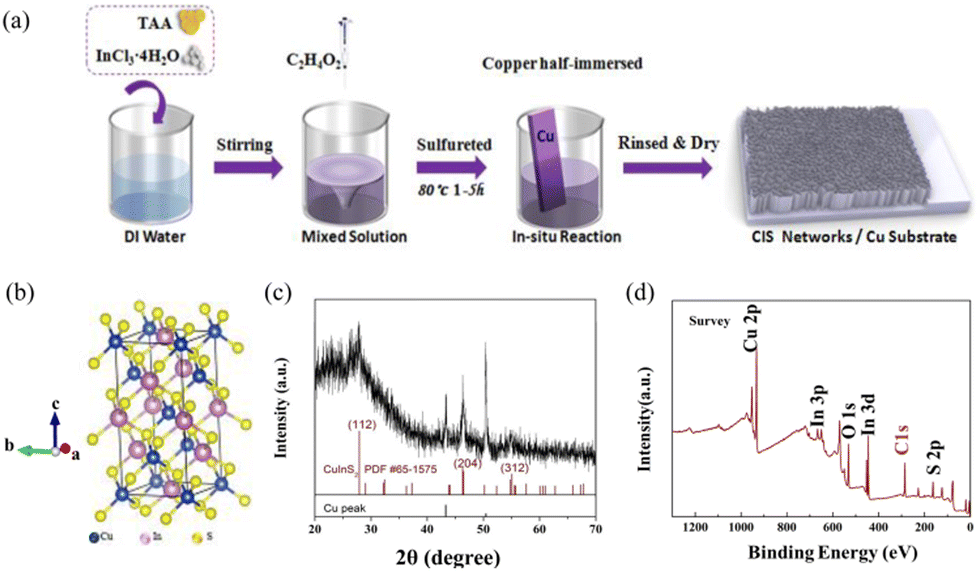 | ||
| Fig. 1 (a) Schematic illustration of the fabrication process of the CIS films. (b) The crystal unit cell structure of the CuInS2 ternary compound. (c) X-ray diffraction spectra of the prepared CuInS2 films. (d) XPS survey spectra of the as-grown CuInS2 sample. | ||
The X-ray diffraction (XRD) patterns of the as-fabricated CIS films are shown in Fig. 1(c). Apart from the two existing evident sharp peaks from the pure Cu (marked by black drop lines), the diffraction peaks at 27.8°, 46.3° and 55.1° are assigned to the (112), (204) and (312) planes of the chalcopyrite-type CIS crystal system, respectively (PDF# No. 65-1575), which are consistent with those in the literature,32 confirming that the chalcopyrite structure CuInS2 (a = 5.523 Å) was successfully prepared. The corresponding crystal unit cell is simulated in Fig. 1(b). The structure is based on the tetrahedral stacking arrangement. Specifically, taking the S atom as the center of the tetrahedron, two of its four corner vertices are occupied by the metal Cu. The other two vertices are occupied by In atoms. Each Cu and In as a shared atom is bonded to one other S element throughout the unit. X-ray photoelectron spectroscopy (XPS) was employed to analyze the surface composition of CIS. As shown in Fig. 1(d), the survey spectrum indicates that the sample contains Cu, In, S elements and O from surface absorption. The high resolution XPS results of the Cu 2p, In 3d and S 2p core levels of the individual elements are displayed in ESI,† Fig. S1. In detail, the core Cu 2p splits into Cu 2p3/2 (932.5 eV) and Cu 2p1/2 (952.5![[thin space (1/6-em)]](https://www.rsc.org/images/entities/char_2009.gif) eV) peaks, which are in good agreement with the reported values for Cu+ (Fig. S1a, ESI†).33 The binding energies of the In 3d5/2 and 3d3/2 peaks are located at 444.7 eV and 452.3 eV with a peak splitting of 7.6 eV, confirming the trivalent In3+ state (Fig. S1b, ESI†). The S 2p has doublet peaks of S 2p1/2 and 2p3/2 due to spin–orbit coupling.34 The two peaks of S 2p (Fig. S1c, ESI†) are located at 161.9 eV (S 2p1/2) and 163 eV (S 2p3/2) with a peak splitting of 1.1 eV, which can be assigned to S2−. No obvious impurities could be detected in the sample.
eV) peaks, which are in good agreement with the reported values for Cu+ (Fig. S1a, ESI†).33 The binding energies of the In 3d5/2 and 3d3/2 peaks are located at 444.7 eV and 452.3 eV with a peak splitting of 7.6 eV, confirming the trivalent In3+ state (Fig. S1b, ESI†). The S 2p has doublet peaks of S 2p1/2 and 2p3/2 due to spin–orbit coupling.34 The two peaks of S 2p (Fig. S1c, ESI†) are located at 161.9 eV (S 2p1/2) and 163 eV (S 2p3/2) with a peak splitting of 1.1 eV, which can be assigned to S2−. No obvious impurities could be detected in the sample.
To further explore the synthesis mechanism during the vulcanization process, the morphology of the copper indium disulfide was characterized as shown in Fig. 2. The morphologies of the CIS samples were characterized by scanning electron microscopy (SEM) and transmission electron microscopy (TEM). Specifically, Fig. 2(a) shows that the large-area resultant film with a net-like porous structure was fabricated, which is built by a great density of CIS nanosheet arrays. Furthermore, the high-magnification SEM image in Fig. 2(b) exhibits the features of the densely packed nanosheets. These CIS photochip-shaped nanoflakes with a vertical growth direction are assembled and inter-meshed with each other, and uniformly covered over the entire surface of the Cu substrate. This could be attributed to the Cu foil directly serving as the copper source, thus leading to the in situ growth of the CIS nanosheet alignments. Moreover, the individual nanosheet displayed a crooked shape with a thickness of ∼25 nm and length in the micron range. A large quantity of the nanosheets were self-supported and well aligned to form the whole CIS film. Fig. S2 (ESI†) reveals the cross-section SEM view of the CuInS2 film on the substrate, confirming that the dense CIS nanosheet arrays are nearly perpendicularly grown and with a thickness in the micrometer size under a condition of 4 h vulcanization. The reaction time plays a vital role in determining the ultimate morphology structure, as a longer time would lead to a second phase forming on the original CIS film, as shown in Fig. S6 (ESI†). In fact, the overall growth process of the CIS nanosheets on copper can be divided into two stages with different growth mechanisms depending on various reaction times, as illustrated in Fig. S3 and S6 (ESI†). At the early stage of the reaction, the CIS mainly undergoes heterogeneous nucleation based on the roughness fluctuations on the surface of the copper sheet to form a uniform CIS nanosheet network layer. After the subsequent saturation of the nucleation sites, the homogeneous nucleation process dominates. The nanoflower ball structure by CIS nanosheets is then formed and assembled on the former layer. In addition, to obtain isolated nanosheets for further exploration, the copper substrate with CIS film is ultra-sonicated and then collected for TEM characterization. The results of the dissociated nanoflake and some peeled fragments are shown in Fig. 2(c). The nanosheet presents a clear square laminar shape slice with a length of ∼7 μm and width of ∼4 μm. Its high-resolution TEM image reveals the evident stratified structure, which is in agreement with the layered feature of the copper chalcogenides (Fig. 2(d)).
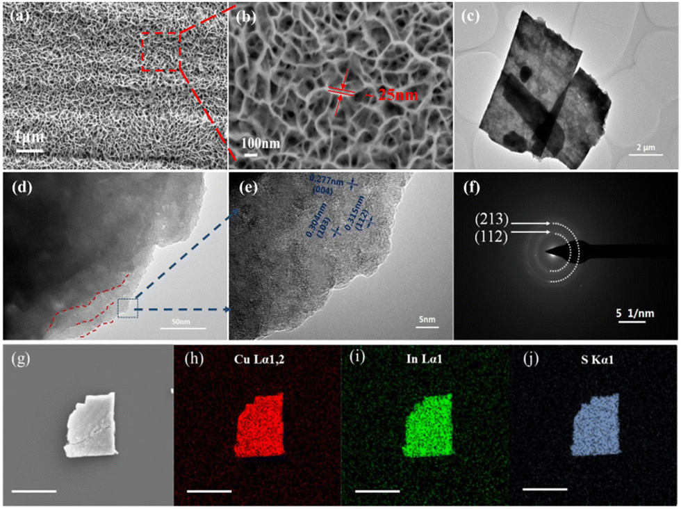 | ||
| Fig. 2 (a) SEM top view image of the CIS nanosheets layer after 4 h reaction. (b) High-magnification SEM image of the marked area in (a). (c) TEM characterization of the CIS nanosheets. (d) HRTEM of the polycrystalline CuInS2 nanosheet in (c) with the flake boundary of the layered feature outlined by dotted lines. (e) Magnified HRTEM view of the marked area in (d) with a polycrystalline feature by varying the lattice orientations. Here, the lattice spacings are measured to be 2.77 Å, 3.04 Å, and 3.15Å. (f) The electron diffraction pattern with the well-indexed (112), (213) planes. (g) SEM image of the CuInS2 nanosheet. (h)–(j) SEM-EDS elemental mapping of the CIS nanosheet fragment of (g); the unit scale is 10 μm. | ||
With the magnified view of the layers margin in the marked area, we get several lattice spaces that are measured to be around 3.15 Å, 2.77 Å and 3.04 Å, corresponding respectively to the (112), (004)/(200), (103) planes of the CuInS2 crystal, as shown in Fig. 2(e). The diffraction ring in Fig. 2(f) shows the polycrystalline feature of the as-synthesized chalcopyrite CuInS2. Simultaneously, the quantitative energy dispersive X-Ray spectroscopy (EDX) analysis was conducted over the margin of the pieces. Only Cu, In and S signal peaks are observed. With the atomic ratios listed in Table S1 (ESI†), it was found that copper had the highest content percent among the elements, which mainly originates from the Cu-rich substrate. When the nanosheet broke away from the metal substrate, the fracture edge would inevitably take the copper growth site off, contributing to the abundance of Cu. Particularly, the atomic compositions of In (13.2%) and S (26.57%) is calculated to have the stoichiometric ratio of 1:2, indicating that the composition of the as-synthesized product is the copper-rich CuInS2. The SEM-EDS elemental mapping images of the CIS chips, as shown in Fig. 2(g)–(i), also confirm that the Cu, In, and S are uniformly distributed over the entire nanosheets. Overall, these results demonstrate that the structure of the vertically grown nanosheet arrays of CIS are successfully formed on the substrate. Remarkably, the Cu substrate not only serves as nucleation sites and a copper source for CuInS2 growth, but also simplifies the procedure of constructing a bottom electrode from device manufacturing.
The device structure of the Cu/CuInS2/Au memristor is shown in Fig. 3(a). Typical I–V characteristics were carried out under DC voltage bias sweeping in a routine of 0 V → +1.0 V → 0 V → −1.0 V→ 0 V, as shown in Fig. 3(b). The current compliance was initially set to 10 mA to prevent the permanent breakdown of the cells. An obvious and uniform bipolar resistive switching behavior was observed, which implies that the switching mechanism was dominated mainly by the ion migration feature, instead of the Joule-heating-based type.9 Within the above sweeping cycle, the positive forward sweeping from 0 to 1.0 V led to an abrupt resistance change at around 0.4 V. This corresponded to the switching from high-resistance (HRS) to low-resistance (LRS), and it remained at LRS, i.e., ‘ON’ state in the back sweeping process to 0 V. Meanwhile, during application of the negative voltage sweeping from 0 to −1.0 V, the LRS state remained until the Reset voltage occurred at about −0.5 V. This marked the switching off from the LRS to HRS states. The RESET process also was marked with an obvious change, as observed in the curve. Notably, the device SET power consumption is only ∼100 pW (PSET = VSET × ISET). This is much lower than many of the reported memristors, and has great potential in developing a low-power electronic device.8
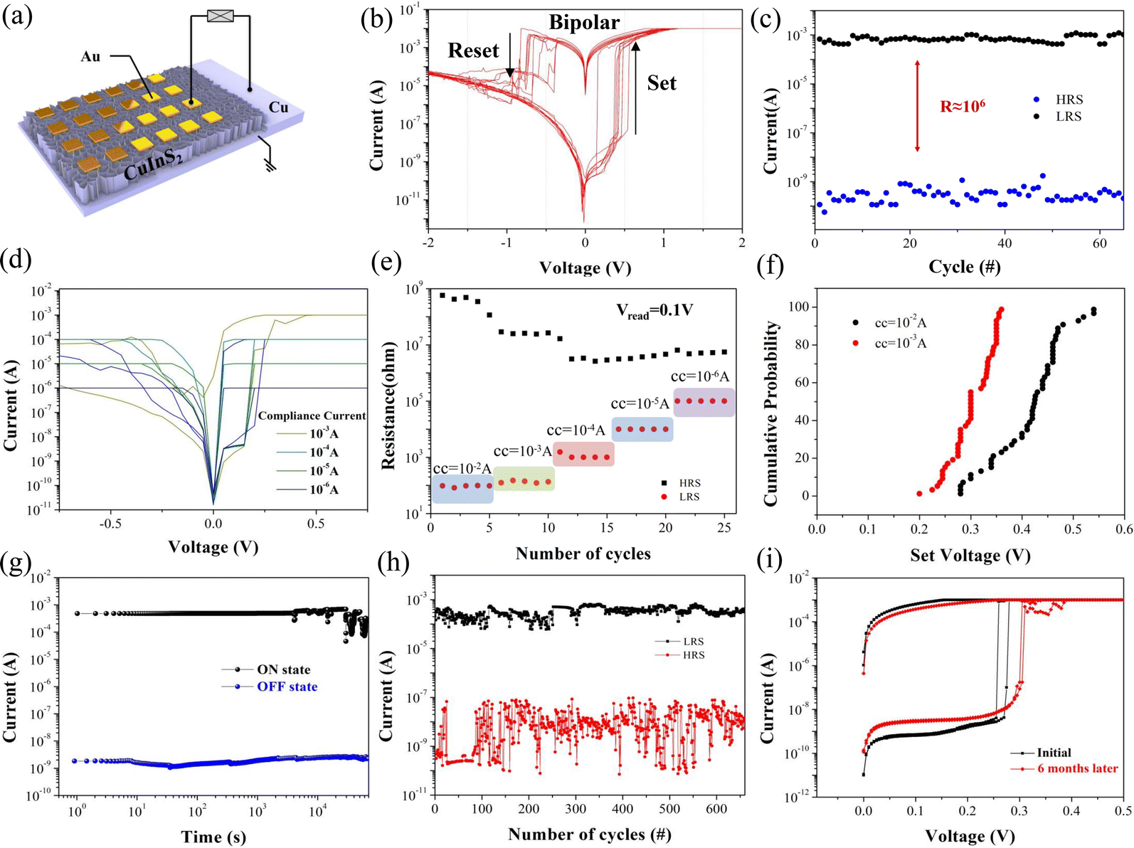 | ||
| Fig. 3 (a) Schematic structure of the Cu/CuInS2/Au resistive switching memory arrays with a Au area of 50 × 50 μm2 each. (b) Repeatability of the bipolar resistive switching behavior of the device evaluated by repeating the I–V characteristics for the first consecutive 20 cycles under the Icc of 10 mA with a sweeping route of 0 V → +1.0 V → 0 V → −1.0 V → 0 V. (c) Statistics distribution of HRSs and LRSs under a read voltage of 0.1 V. (d) I–V curve characterization of the Cu/CuInS2/Au devices with different current compliances. (e) Statistics distribution of HRSs and LRSs under a series of current compliance, and each for 5 cycles. (f) Statistic set voltage threshold distributions under Icc of 10 mA and 1 mA. (g) Retention time characterization over 104 s. (h) Statistics of the value changes of HRSs and LRSs during the endurance test read at 0.1 V by applying 0.5 V/0.1 V/−0.5 V/0.1 V sequence pulses under the Icc = 1 mA. (i) Stability test of the representative Write I–V curves of the device before and after 6 months under the air condition. | ||
From each periodic I–V characterization, the paired data points of HRSs and LRSs were collected from over 60 cycles at a reading voltage of 0.1 V, as displayed in Fig. 3(c). Good fidelity and a large ON/OFF ratio window of ∼106 are observed in the CIS memristor, indicating that a very low misreading possibility can be guaranteed during the read operations. Multilevel resistance states could also be achieved with compatible different compliance current (denoted as CC) values. Here, different CCs (CC = 10−6; 10−5; 10−4; 10−3 A) were previously set in the test circuit, and the corresponding I–V curves are plotted in Fig. 3(d). It is well known that one memory device with multilevel resistance states could provide the feasibility of an ultra-high data storage density by representing multiple data bits in one single cell, when compared to the ordinary binary states of HRS and LRS only. In Fig. 3(e), the multiple resistance states are obtained under these CC levels (each repeated for 5 cycles). It is evident that the LRSs present a step rise regularity with increasing Icc value, resulting in the window decrease of the ROFF/RON. Overall, the clear distinction under different Icc exhibits great potential of CIS in multi-value storage application. It has also been reported that the low resistance state of the filaments inside the material connecting the pair electrodes is largely decided by the highest current level through the device. A larger CC would contribute to a more robust filament. This also requires more effort to melt down or dissipate the ion filaments in RESET operation. Therefore, a smaller value of the SET/RESET voltage might be achieved when CC diminishes since a thinner filament would require easier formation, leading to the decrease of the SET voltage. It has been reported that a linear relationship exists between the SET power and the applied Icc, which suggests an effective approach to further decrease the power consumption by means of reducing the Icc. So, a balance should be considered for the memristor in choosing an appropriate Icc value that could be energy efficient and still exhibit a high on-off ratio. Fig. 3(f) gives the statistic distribution of the set voltages under Icc = 10 mA and Icc = 1 mA for 50 I–V sweeping cycles. The results indicate that the smaller limiting current leads to relatively lower and centralized operating voltage distribution range, where the VSET (Icc = 1 mA) is distributed in the small range of 0.20 to 0.35 V and concentrated around 0.3 V. Further reduction of the CC value would only slightly tune the operation voltage. A distinction is still necessary between the set voltage and read voltage value of 0.1 V. Therefore, the value of 1 m A would be a suitable limit for our device with a large on-off ratio and low power consumption achieved for our device, and could be applied for subsequent characterization.
The reliability of the CIS is another very important figure of merit. Specifically, the data retention time and switching endurance are essential evaluations, and are presented in Fig. 3(g) and (h), respectively. The endurance is measured by applying ac voltage sequences of 0.5 V/0.1 V/−0.3 V/0.1 V pulses and 30 ms pulse duration, which keeps the device in a process of cyclical memristive switching. The cycle endurance can reach over successive 500 cycles. The HRSs and LRSs values have been carefully extracted at 0.1 V, and are plotted in Fig. 3(h). The HRSs exhibit a highly repeatable feature and good on-off difference, although they have a relative larger fluctuation than the LRSs. This can be attributed to the stochasticity rupture of the conducive filaments (CFs). The residual CFs existing in the device with different degrees after the RESET operation would result in the phenomenon of the HRSs having a larger fluctuation. Moreover, a long-term resistive retention time of over 104 s is obtained, as shown in Fig. 3(g). The devices maintained a ∼106 ON/OFF ratio for more than 6 months in an ambient environment, as shown in Fig. 3(i); this indicated the typical favorable environmental stability of the copper chalcogenides. The overall performance of our CIS memristor is better than that of many other chalcogenide film-based memristors in the literature reports, as shown in Table S2 (ESI†). Especially when compared with the CuInX2 (X = Te, Se, S) series switching layer in the form of a bulk film,31 the stability and retention time have significantly improved in this work. This is obviously beneficial from the extremely efficient isolation of leakage paths by our unique film structure of vertical nanosheet arrays.
We further explored the relationship between the synthesis and materials properties, as illustrated in Fig. S4 (ESI†). We have achieved the scalable and controllable growth of the CIS nanosheet network, and unfolded its impact on the memristive on-off value, facilitating the optimization of the device performance in terms of the switching medium composite. The results indicate that the CIS with a ∼4 h reaction time exhibits the largest ROFF/RON. More details are shown in the ESI.†
To study the resistive switching mechanism of Cu/CIS/Au, the HRS and LRS of the I–V curve in the positive voltage formation region were fitted, as shown in Fig. 4(a). Obviously, the LRS region possesses the linear fitted slope of ∼1, which is in accordance with the Ohmic conduction. With regard to the HRS region, the unusual I–V relationship is required for further curve fitting. Their linear function between ln(I/V) and V1/2 satisfies the Pool—Frenkel (PF) conduction principle, as specifically illustrated in Fig. 4(b). The PF effect is also called the Field-assisted thermal ionization, which is generated from quantities of defects inside the material. These defects could trap or release electrons working as numerous Coulomb potential barrier traps, which can adjust the electron concentration and change the conductance of the material. With the action of an external electric field, the energy barrier could be further lowered to promote the electron transition to a conduction band. The I–V characterization curve thus satisfies the following relationship:
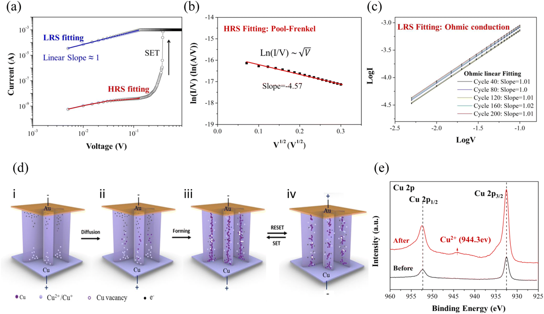 | ||
| Fig. 4 (a) Typical I–V curve of the CIS-based memristor for fitting. (b) Switching mechanism fitting of the HRS under the positive voltage. (c) Switching mechanism fitting of the LRS under the positive voltage. (d) Schematic model of the working mechanism of the Cu/CuInS2/Au Re-RAM devices. (e) XPS results of the Cu element in the original CIS, and after the operation of resistive switching. | ||
As is widely accepted, the electrochemical metallization (ECM) mechanism of Cu is reflected in the migration of metallic copper cations inside the electrolyte. The applied electrical field is the key to driving the migration of ions to form the conductive channels. To confirm the switching phenomena of the CIS film under a voltage bias, the conductive-atomic force microscope (C-AFM) characterization was first implemented, as shown in Fig. S9 (ESI†). The in situ current mapping under LRS and HRS were compared. The LRS state exhibits a much denser current distribution throughout the whole film, which is attributed to the formed conducive channels. It is known that the quantities of ions and vacancies in the polycrystalline CIS would enable the formation of CFs for resistive switching (RS) behavior. For further analysis, a resistive switching model related to these impurities and defect states is shown in Fig. 4(d). As shown in the schematic model, the defects-induced nature combined with ion migration are deduced to be responsible for the resistive mechanism of CIS as follows. In the tested vertical copper indium sulfide nanosheets layer, the positively charged Cu ions are driven by the external electric field as the key switching species. When the positive voltage is applied as the direction of (i), many Cu atoms from the copper substrate are oxidized into Cu2+ ions and then penetrate the CIS layer, followed by diffusion toward the counter electrode under an external voltage (ii). Meanwhile, the electrons coming mainly from the Au move in the opposite direction. These electrons reduce the ions subsequently in the migration path with the electric field, which is the process of their being trapped or released by these positive ion defects along the route to control the electron concentration in the layer. Thus, the reduced copper atoms disperse along the channel and aggregate to form the copper filaments. When the voltage reaches the threshold, a fiber composed of metallic Cu would ultimately bridge the Cu and Au electrodes as shown in (iii), resulting in the LRS state with Ohmic conduction. For experimental verification, 200 cycles were conducted to analyze the LRS curve feature, as shown in Fig. 4(c). The lg(I) and lg(V) were found to be proportionally related by ∼1, confirming the Ohmic contact resulting from the copper filament. When the reverse direction of the electrical field is implemented as the RESET operation in (iv), the electrons are drawn back. The Cu atoms of the filament are oxidized back to ions and dissipate. This leads to the rupture of the conducting channel, and then the resistance increases. Similarly, to repeat the SET process, the opposite polarity voltage was used to reconstruct the filament. To further confirm that the active metallic copper plays a role in electrical metallization process, the XPS characterization of the Cu element in CIS was compared before and after the device switching operation, as shown in Fig. 4(e). With the freshly fabricated CIS layer on the Cu substrate, the Cu 2p shows only Cu 2p3/2 (932.5 eV) and 2p1/2 (952.5 eV) corresponding to Cu+. After the resistive switching endurance characterization, a new satellite peak at about 944.3 eV appears in the result. This corresponds to the characteristic peak of Cu2+, indicating that the Cu2+ ions exist during the switching process and the oxidization reaction happened, which verified the credibility of the Cu-based switching species of our model. The oxidized Cu2+ is derived from two sources of copper. The active metal copper substrate also serves as an electrode, which offers a consistent source of Cu atoms under a forward voltage. On the other hand, the intrinsic Cu+ inside the CIS material could be oxidized to Cu2+ or reduced to zero valence. This is driven by the applied voltage due to the low formation energy and easily mobile nature of the Cu vacancies in the copper chalcogenides, which are a positively conductive species. Actually, the copper filaments are composed of two kinds of copper species, i.e., copper atoms and copper vacancies. As a recent research study has reported,8 the memristive behavior is the innate genuine nature of the 2D copper chalcogenides, which is just like the oxygen vancancies for conventional memristive metal oxides. The inherent copper ions create innumerable ion transport channels, which results in the small switching threshold voltages, good reproducibility and stable retention performance in CIS.
To further demonstrate the application of the information write/erase function of the Cu/CIS/Au memory device, we have chosen device cell group combination to physically achieve the character strings storage. The information type of picture would be practiced for more intuitive illustration. An array composed of 3 × 4 memory cells was selected to record one simple image information of letter “T”, as displayed in Fig. 5(c). Every cell would be defined with a binary value of 0 or 1 and combined wholly in the shape of “T”, where the LRS is 1 and the HRS is 0. First, 15 pixel cells (Fig. 5(a)) were individually performed with I–V characterization (Fig. 5(b)). The uniform bipolar switching curves indicate that these memristor cells are independent of each other. It should be noted that each microscale top-evaporated electrode would cover quantities of vertical nanosheets with nano-thickness. The minimum top area of the device unit is actually limited by the tested probe diameter. Each vertical nanosheet is one complete memristor device with highly dense aggregates. So, to ensure that the operating nanosheets are consistent with the final tested probe left the cell top electrode, we used metal lines for the external extension with fixed ends on each top cell of the 3 × 4 group. Then, a small reading voltage of 0.1 V is applied to the 12 pixel cells to check the initial states, as shown in Fig. 5(d). The 12 HRSs are thus distributed and ready for storage.
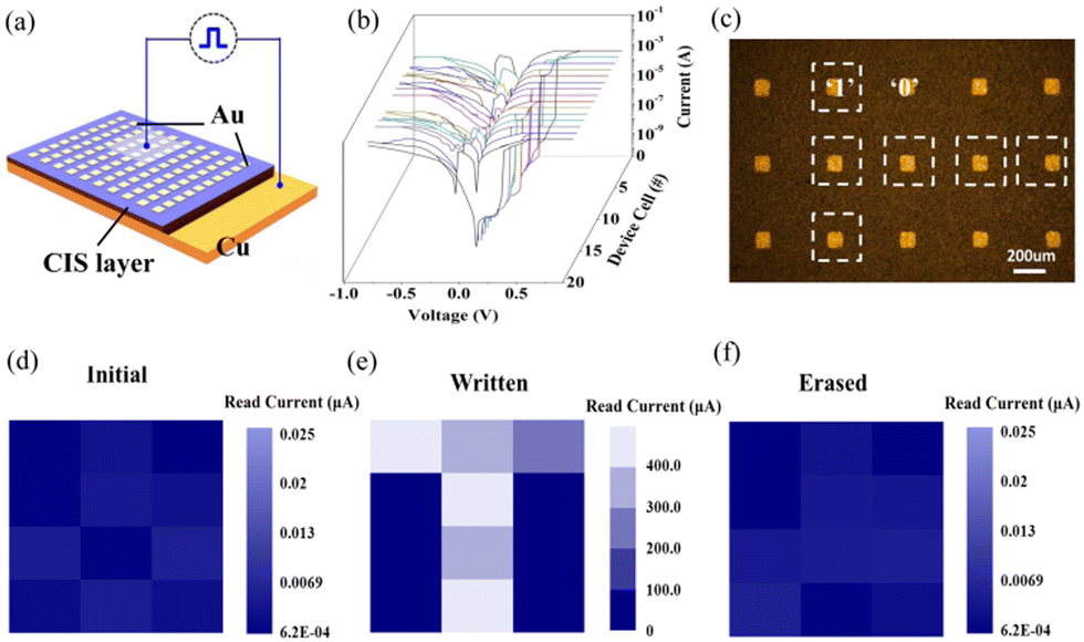 | ||
| Fig. 5 (a) Test device schematic view of the selection area. (b) Individual original I–V characterizations of the 15 cell devices. (c) Pre-chosen area array for the pattern of “T”. (d)–(f) Resistance distribution mapping of the 3 × 4 arrays as the initial, written and erased states, respectively. | ||
The currents under the reading voltage from each cell were mapped, and are presented in a sequence of color saturation contrast. After that, electrical pulses were given to the respective pixel cells for write operation by level of 0.5 V/0.1 V (Fig. S8a, ESI†) to achieve the selective set. Here, one patterned image of “T” was preset into the memory device, followed by applying the reading voltage of 0.1 V. The resistance states were then read out to constitute the complete image information “T”, as shown in Fig. 5(e). The successful reproduction of the image in the 3 × 4 array with only via a small reading voltage proved the effective written operation. As expected, when the 3 × 4 array was applied with negative RESET voltage pulses for erase operation (Fig. S8b, ESI†), the resultant image of the letter “T” was cleared from the memory device. The device returned to its pristine state, where no information was stored, as illustrated in Fig. 5(f). Overall, the accomplishment of data writing and erasing operation confirms the practical application of the CIS-based memory device, which proves the high potential for application in other memory integration device systems.
Conclusions
In summary, we have successfully synthesized CuInS2 nanosheet arrays via the low-cost, facile and feasible fabrication method of in situ vulcanization on a copper substrate. The intrinsic nonvolatile memristive behaviors of the CuInS2 nanosheet array film were investigated for the first time. With the unique vertical 2D network structure, the memristor of Cu/CIS/Au exhibits a relatively small switching voltage (∼±0.3 V), large ON/OFF ratio (∼106), long data retention time (>104 s), reliable repeatability and superior device independence in one film. Multilevel resistances have been demonstrated for up to five levels by varying the compliance currents, significantly enhancing the data storage density. In addition, the switching mechanism model of the Cu ECM effect has been explained and proved. For application, we successfully visualized the memory operation of Write/Erase with the image pattern based on the CIS memristor arrays. This work provides a deep understanding of the memristive behavior within the copper chalcogenide family, and may provide new opportunities of developing next-generation storage electronics with high-performance and low power consumption.Author contributions
Zijun Hu and Fa Cao: conceptualization, methodology, investigation, data curation, writing – original draft. Tingting Yan and Li Su: data curation and visualization. Xiaosheng Fang: supervision, conceptualization, writing – review & editing.Conflicts of interest
There are no conflicts to declare.Acknowledgements
This work is supported by the National Key R&D Program of China (No. 2022YFA1402900), National Natural Science Foundation of China (No. 12061131009 and 51872050), the Young Scientist Project of MOE Innovation Platform, the China Postdoctoral Science Foundation (2022M710710), and the Science and Technology Commission of Shanghai Municipality (No. 21520712600 and 19520744300).Notes and references
- S. Ali, S. Khan, A. Khan and A. Bermak, IEEE Access, 2021, 9, 95970–95985 Search PubMed.
- L. Gao, Q. Ren, J. Sun, S. T. Han and Y. Zhou, J. Mater. Chem. C, 2021, 9, 16859–16884 RSC.
- Q. Zhao, Z. Xie, Y. P. Peng, K. Wang, H. Wang, X. Li, H. Wang, J. Chen, H. Zhang and X. Yan, Mater. Horiz., 2020, 7, 1495–1518 RSC.
- Y. H. Chen, L. X. Su, M. M. Jiang and X. S. Fang, J. Mater. Sci. Technol., 2022, 105, 259 CrossRef.
- Y. Hu, S. Zhang, X. Miao, L. Su, F. Bai, T. Qiu, J. Liu and G. Yuan, Adv. Mater. Interfaces, 2017, 4, 1700131 Search PubMed.
- C. Gu and J. S. Lee, ACS Nano, 2016, 10, 5413–5418 CrossRef CAS PubMed.
- Y. Gong, Y. Wang, R. Li, J. Q. Yang, Z. Lv, X. Xing, Q. Liao, J. Wang, J. Chen, Y. Zhou and S. T. Han, J. Mater. Chem. C, 2020, 8, 2985–2992 RSC.
- L. Yin, R. Cheng, Y. Wen, B. Zhai, J. Jiang, H. Wang, C. Liu and J. He, Adv. Mater., 2022, 34, 2108313 CAS.
- Y. Chen, IEEE Trans. Electron Devices, 2020, 67, 1420–1433 CAS.
- T. Gao, Q. Zhang, L. Li, X. Zhou, L. Li, H. Li and T. Zhai, Adv. Opt. Mater., 2018, 6, 1800058 Search PubMed.
- L. Wang, P. Hu, Y. Long, Z. Liu and X. He, J. Mater. Chem. A, 2017, 5, 22855–22876 CAS.
- K. Ramasamy, H. Sims, W. H. Butler and A. Gupta, J. Am. Chem. Soc., 2014, 136, 1587–1598 CAS.
- N. V. Melnikova, Y. A. Kandrina, A. V. Tebenkov, E. A. Stepanova, A. N. Babushkin, A. Y. Mollaev, L. A. Saipulaeva and A. G. Alibekov, Phys. Solid State, 2017, 59, 89–92 CAS.
- O. Pyatilova, S. Gavrilov, R. Rozanov, A. Zheleznyakova, A. Belov and V. Shevyakov, in International Conference on Micro- and Nano-Electronics 2014, 2014, 9440, 944007.
- X. Shi, S. Jiang, H. Yin, J. Zhao and G. Zhao, Phys. Status Solidi RRL, 2021, 15, 2100304 CAS.
- M. Congiu, L. G. S. Albano, O. Nunes-Neto and C. F. O. Graeff, Electron. Lett., 2016, 52, 1871–1873 CAS.
- H. J. Hovel and J. J. Urgell, J. Appl. Phys., 1971, 42, 5076–5083 CAS.
- X. Guan, Z. Lei, X. Yu, C. H. Lin, J. K. Huang, C. Y. Huang, L. Hu, F. Li, A. Vinu, J. Yi and T. Wu, Small, 2022, 18, 2203311 CAS.
- L. Yin, L. Yin, R. Cheng, R. Cheng, Z. Wang, Z. Wang, F. Wang, M. G. Sendeku, M. G. Sendeku, Y. Wen, X. Zhan, J. He, J. He and J. He, Nano Lett., 2020, 20, 4144–4152 CAS.
- M. Wang, S. Cai, C. Pan, C. Wang, X. Lian, Y. Zhuo, K. Xu, T. Cao, X. Pan, B. Wang, S. J. Liang, J. J. Yang, P. Wang and F. Miao, Nat. Electron., 2018, 1, 130–136 CAS.
- Y. Yang, H. Du, Q. Xue, X. Wei, Z. Yang, C. Xu, D. Lin, W. Jie and J. Hao, Nano Energy, 2019, 57, 566–573 CAS.
- S. Chen, M. R. Mahmoodi, Y. Shi, C. Mahata, B. Yuan, X. Liang, C. Wen, F. Hui, D. Akinwande, D. B. Strukov and M. Lanza, Nat. Electron., 2020, 3, 638–645 CAS.
- V. K. Sangwan, D. Jariwala, I. S. Kim, K. S. Chen, T. J. Marks, L. J. Lauhon and M. C. Hersam, Nat. Nanotechnol., 2015, 10, 403–406 CAS.
- F. Zhang, H. Zhang, S. Krylyuk, C. A. Milligan, Y. Zhu, D. Y. Zemlyanov, L. A. Bendersky, B. P. Burton, A. V. Davydov and J. Appenzeller, Nat. Mater., 2019, 18, 55–61 CAS.
- V. K. Sangwan, H. S. Lee, H. Bergeron, I. Balla, M. E. Beck, K. S. Chen and M. C. Hersam, Nature, 2018, 554, 500–504 CAS.
- X. Wang, B. Wang, Q. Zhang, Y. Sun, E. Wang, H. Luo, Y. Wu, L. Gu, H. Li and K. Liu, Adv. Mater., 2021, 33, 2102435 CAS.
- H. Zhao, Z. Dong, H. Tian, D. DiMarzi, M. Han, L. Zhang, X. Yan, F. Liu, L. Shen, S. Han, S. Cronin, W. Wu, J. Tice, J. Guo and H. Wang, Adv. Mater., 2017, 29, 1703232 Search PubMed.
- Y. K. Wang, Y. L. Li and Y. N. Gao, Chin. Opt., 2021, 14, 18–42 CAS.
- M. Tang, Q. Tian, X. Hu, Y. Peng, Y. Xue, Z. Chen, J. Yang, X. Xu and J. Hu, CrystEngComm, 2012, 14, 1825–1832 CAS.
- Z. Chen, M. Tang, L. Song, G. Tang, B. Zhang, L. Zhang, J. Yang and J. Hu, Nanoscale Res. Lett., 2013, 8, 1–8 Search PubMed.
- T. Ahmad, W. Devulder, K. Opsomer, M. Minjauw, U. Celano, T. Hantschel, W. Vandervorst, L. Goux, G. S. Kar and C. Detavernier, ACS Appl. Mater. Interfaces, 2018, 10, 14835–14842 CAS.
- P. K. Santra, P. V. Nair, K. George Thomas and P. V. Kamat, J. Phys. Chem. Lett., 2013, 4, 722–729 CAS.
- J. Llanos, A. Buljan, C. Mujica and R. Ramírez, J. Alloys Compd., 1996, 234, 40–42 CAS.
- W. Chen, Z. Wan, W. Cao, C. Dong, J. Chen, R. Liu, L. Zhu, X. Zhang and M. Wang, Mater. Lett., 2021, 290, 129490 CAS.
Footnotes |
| † Electronic supplementary information (ESI) available. See DOI: https://doi.org/10.1039/d2tc04003d |
| ‡ These authors contributed equally to this work. |
| This journal is © The Royal Society of Chemistry 2023 |