 Open Access Article
Creative Commons Attribution 3.0 Unported Licence
Chirality and length-dependent electron transmission of fullerene-capped chiral carbon nanotubes sandwiched in gold electrodes†
Ameet
Kumar
,
Sudip
Sarkar
 * and
Daeheum
Cho
*
Department of Chemistry and Green-Nano Materials Research Center, Kyungpook National University, Daegu 41566, South Korea. E-mail: sudipchem23@knu.ac.kr; daeheumc@knu.ac.kr; Tel: +82-53-950-6340
First published on 5th January 2024
Abstract
In order to develop high-performance CNT-based electronic and optoelectronic devices, it is crucial to establish the relationship between the electron transport properties of carbon nanotubes (CNTs) and their structures. In this work, we have investigated the transport properties of chiral (8, m) and (10, m) CNTs sandwiched between two gold electrodes by employing nonequilibrium Green's function (NEGF) combined with density functional theory (DFT). We demonstrate that with the change of chirality the transport property changes, as predicted by the (n − m) rule. The change of length is also considered. Our results show that the electrical conductance of (10, m) CNTs is larger than that of the (8, m) CNTs, due to larger diameter. Furthermore, we found that the (8, 1) chiral CNT does not follow the (n − m) rule in shorter length and it shows metallic behavior. The cohesive energy, wavefunctions of electronic states, and coupling energy calculation indicate that the devices considered in this study are stable. The transmission spectra, current vs. voltage curves, and transmission eigenchannels provide strong evidence for our findings. Among the (10, m) series, (10, 3) CNT would be the optimal choice for a semiconducting molecular junction device with a significant conductance of 20 μA at 0.8 bias voltage.
1. Introduction
Carbon nanomaterials have become some of the most investigated nanomaterials in the field of nanotechnology since their discovery by Iijima and Ichihashi because of their outstanding electronic, optoelectronic, and mechanical properties.1–13 Extensive studies in the field of carbon nanotubes (CNTs) during the last decade have resulted in substantial improvements and prospective applications including electronic devices,14 nanoscale sensors,15 separation membranes16 and drug-delivery systems.17Among the carbon allotropes, CNTs have emerged as prominent contenders for potential utilization in forthcoming technological advancements.18,19 By manipulating the rolling direction of a graphene sheet, various types of CNTs can be obtained: armchair (n, n), zigzag (n, 0), and chiral (n, m) nanotubes, where n and m integers are called chiral indices.20–22 Most researchers have focused on understanding the transport features of zigzag (n, 0), and armchair (n, n) CNTs.23–29 There have been fewer works on the chiral CNTs because of their complex structures. An interesting fact is that their electronic properties rely on the shape of CNTs.30,31 When the difference (n, m) is a factor of 3, the chirality of CNT (n, m) imparts a metallic behavior; otherwise, it is semiconducting.32–35
It demonstrates how chirality can significantly affect the electrical characteristics of CNTs.36 The proposal of CNT-based intermolecular junctions was made early on with the aim of integrating CNTs into operational nanodevices such as diodes and transistors. Both experimental and theoretical investigations of these junctions hold great potential.26 The CNTs were sandwiched between the two electrodes to investigate their transport properties. A major prerequisite for establishing a robust connection between the CNTs and the electrodes was to construct a stable geometric arrangement. This was accomplished by capping the CNTs with suitable fullerenes. The proper diameter of the fullerenes was critical in assuring the connection's stability. The major goal regarding these nanodevices was to examine the unique electrical properties of CNTs terminated with fullerene caps.37 The fullerene capping in CNTs could be a promising way to enhance the electron transport. The fullerene capped strategy would create well-defined contact between the electrode and CNTs.
Chirality-dependent electrical transport capabilities of CNTs were experimentally studied by Su et al.38 They evaluated the performance of eleven kinds of (n, m) chiral CNT thin-film transistors to investigate the effect of the chirality of the CNT on electron transport properties. According to them, the on-state current or carrier mobility varies as the chirality even with the same tube diameters. Xu et al. investigated the chirality switched from (6, 5) to (6, 4) by varying the oxidation degree of the catalyst.39 Chirality dependent transport properties of CNTs and SiNTs have also been compared. Jafari et al. suggested the (6, 2) CNTs have semiconducting properties while SiNTs are metallic in nature. Several inorganic elements, such as Cu, Ni, N, and B have been employed to functionalize the CNTs and Stone–Wales defects were also studied to increase the magnetic, energetic and transport properties of CNTs used as molecular junction.40–43 Meena et al. reported the fluorinated zigzag (8, 0) CNT sandwiched between two CrO2 half-metallic-ferromagnetic (HMF) electrodes to analyze the spin transport properties and obtained maximum spin filtering in fluorinated (8, 0) carbon nanotube.29
In this study, we systematically investigated the chirality- and length-dependent electron transport properties of chiral CNT molecular devices using density functional theory (DFT) in conjunction with the nonequilibrium green function (NEGF) technique. We report the transport properties of chiral (8, m) and (10, m) molecular junctions by investigating their transmission coefficients T(E), density of states (DOS), current–voltage (I–V) characteristics, and transmission eigenchannels. To our knowledge, systematic study has not been conducted to understand the electron transport properties of chiral CNTs as a function of the chirality and the length of the tubes. Our findings may provide crucial insights for the design of high-performance carbon-based electronic devices.
2. Computational details
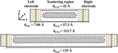
In the molecular junction devices, a chiral CNT terminated with semi-fullerene was sandwiched between the two gold electrodes as shown in Fig. 1 (see Fig. S1 for the geometries of all Au electrode–CNT–Au electrode (Au|CNT|Au) junctions, ESI†). Table 1 lists the tube length, diameter, cohesive energy, coupling energy, and charge transfer analysis of (8, m) and (10, m) CNTs. Chiral CNTs with various chirality and lengths were studied. The geometries of the molecular junctions were optimized using the GFN1-xTB44 level of theory as implemented in the DFTB+ program.45| System | Tube length (S/L) (Å) | Diameter (Å) | Cohesive energy (eV) | Coupling energy (eV) | Charge transfer (e) |
|---|---|---|---|---|---|
| (8, 1) | 42/113 | 6.73 | −9.807/−9.072 | −4.472/−4.461 | 0.773/0.652 |
| (8, 2) | 50/100 | 7.18 | −9.839/−9.863 | −3.349/−3.123 | 0.523/0.463 |
| (8, 3) | 50/91 | 7.72 | −9.863/−9.883 | −3.436/−3.347 | 0.573/0.537 |
| (8, 4) | 53/100 | 8.29 | −9.885/−9.903 | −3.220/−3.121 | 0.726/0.772 |
| (10, 1) | 53/98 | 8.31 | −9.094/−9.894 | −4.789/−4.400 | 2.831/0.961 |
| (10, 2) | 55/102 | 8.71 | −9.112/−9.912 | −3.936/−3.562 | 2.96/0.788 |
| (10, 3) | 58/108 | 9.22 | −9.909/−9.925 | −3.889/−3.730 | 0.963/0.927 |
| (10, 4) | 53/98 | 9.77 | −9.906/−9.932 | −3.936/−3.520 | 0.946/1.199 |
| (8, 0)53 | NA | 6.26 | −9.065 | NA | NA |
| (12, 0)53 | NA | 9.4 | −9.170 | NA | NA |
The electronic transport properties were calculated by employing the NEGF formalism implemented in Spanish Initiative for Electronic Simulation with Thousands of Atoms (SIESTA)/TranSIESTA software.46 We utilized the Perdew, Burke, and Ernzerhof (PBE) generalized gradient approximation47 functional with a DZP Troullier–Martins basis set48 and a 300 Ry mesh cutoff. Although the PBE functional underestimates the bandgap due to self-interaction error, but for qualitative analysis it has been used widely.49–52 The 1 × 1 × 5 K-point sampling method was used throughout the calculation.
The current (I) as a function of bias voltage (Vbias) for the molecular device was determined using the Landauer–Buttiker formalism as follows:
 | (1) |
 | (2) |
For verifying the stability of fullerene-capped CNTs, we have examined the cohesive energy values, and the results are shown in Table 1. Cohesive energy is defined as the amount of energy required to separate the isolated atoms from their condensed phase.
 | (3) |
The coupling energies between the capped CNTs and gold electrodes were determined in order to ensure the stable device as shown in Table 1. The coupling energy was calculated by
| Ecoup = Edevice − (ECNT + Egold) | (4) |
We have also examined the charge transfer from gold electrodes to CNTs, which is given by
| CC.T. = CScat − 4 × nC | (5) |
3. Results and discussion
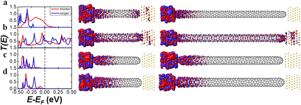
We investigated the chirality- and length-dependent electron transmission properties of chiral (8, m) and (10, m) CNTs listed in Table 1. Here, “8” and “10” indicate carbon atoms around the nanotube circumference, where “m” is an integer to determine the tube's helicity. The (n − m) rule for chiral CNTs predicts semiconductor behavior when (n − m) = 3k + 1 and 3k + 2 and a metallic behavior when (n − m) = 3k, where k is a positive integer. According to the (n − m) rule, chiral (8, 2), (10, 1), and (10, 4) are metallic, while (8, 1), (8, 3), (8, 4), (10, 2), (10, 3) CNTs are semiconducting.We have calculated the T(E) and transmission eigenchannels of (8, m)S systems with shorter length ∼50 Å as shown in Fig. 2 (see the density of states in Fig. S2 in the ESI†). The (8, 1)S and (8, 2)S CNTs have significant T(E) values at the Ef, thus metallic behavior, while the (8, 3)S and (8, 4)S CNTs the negligible T(E) values, thus the semiconducting or insulating behavior. The metallic behavior of the (8, 1)S contradicts the (n − m) rule, predicting the semiconducting behavior. The discrepancy can be understood from the tunneling behavior of the (8, 1)S as discussed in the next paragraph.
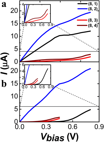
The transmission eigenchannels at the Ef of the (8, 1)S and (8, 2)S (Fig. 2a and b middle) were well-delocalized over the molecular junction, indicating the metallic behavior. More interestingly, the quantum tunneling was found in the transmission eigenchannel of the (8, 1)S, which results in the metallic transport property. The transmission eigenchannels at the Ef of the (8, 3)S and (8, 4)S are localized to the left electrode, resulting in a semiconducting behavior. As shown in Fig. 4, the I–V curve of (8, 1)S and (8, 2)S CNTs revealed the metallic character, while the (8, 3)S and (8, 4)S the semiconducting behavior, as expected from the Fig. 2.
The (8, 1)S exhibits strong coupling energy than the other (8, m)S systems with gold electrodes and thus shows the larger conductance as shown in Table 1.55 The coupling energy values are decreases with increasing length. Furthermore, the wavefunctions of (8, m)S systems were calculated near the Ef and shown in Fig. 3. In chiral (8, 1)S, the wavefunctions of VBM (Valence Band Maximum) and CBM (Conduction Band Minimum) are well-delocalized over the entire CNT. As a consequence, the (8, 1)S system shows metallic properties and higher conductance. In (8, 2)S system, the wavefunctions of VBM and CBM are also well delocalized which strongly supports the metallic behavior of the system. While in semiconducting systems (8, 3)S and (8, 4)S the wavefunctions of VBM and CBM are not well delocalized over the CNT which exhibits lower conductance. (For other wavefunctions of the electronic states see Fig. S3–S6 in ESI.†) The CBM + 1 and CBM + 2 of (8, 1)S (Fig. S3, ESI†) are also delocalized over the entire CNT which confirms the metallic nature while in (8, 3)S and (8, 4)S (Fig. S5 and S6 ESI,† respectively) the delocalization was not observed which shows the semiconducting properties. Furthermore, the charge transfer analysis of (8, m) has also been carried out and shown in Table 1 and charge transfer is observed from electrode to scattering region, in all the systems.
The charge transfer of (8, 1)S/L are observed as 0.773/0.652 (e). In (8, 2)S/L the charge transfer is 0.523/0.463 (e). Besides in (8, 3)S/L the charge transfer is obtained as 0.573/0.537 (e). While in (8, 4)S/L the charge transfer is 0.726/0.772 (e). It can be noticed that the charge transfer is decreased by increasing the length in all three systems except (8, 4)S/L. The charge transfer increases with the coupling energy between the electrode and scattering region except (8, 4)S/L.
The strong overlap between wavefunctions of the electrode and scattering region, noticed in all the systems (Fig. 3), suggests that the charge transferred from the left electrode to scattering region which supports strong coupling.56
We have analyzed the length-dependent transport property of the (8, m) CNTs by comparing the shorter (8, m)S and the longer (8, m)L CNTs. Generally, the transmission T(E) and the conductance would decrease upon the length.57,58 The T(E) curves at the Ef of chiral (8, 1), (8, 3), and (8, 4) decreased with increasing length as shown in Fig. 2. The T(E) value at the Ef of chiral (8, 1)L is significantly decreased as compared to the (8, 1)S, because the quantum tunneling is suppressed in the (8, 1)L. Indeed, the transmission eigenchannel at the Ef of the (8, 1)L does not exhibit quantum tunneling (Fig. 2a right panel). Therefore, the (8, 1)L exhibits semiconducting behavior, while the (8, 1)S shows metallic behavior. The length-dependent transmission property of the (8, 1) CNT suggests a new approach to control the transport property of chiral CNTs with tube length. In contrast to the dramatic length-dependent transport property of the (8, 1), the (8, 2), (8, 3), (8, 4) CNTs do not show significant length-dependency. The (8, 2)S and (8, 2)L exhibits comparable T(E) values, transmission eigenchannel, and thus the metallic behavior and the similar I–V curve regardless of the length of the CNTs. The I–V curves of the (8, 3)L and (8, 4)L were obtained up to Vbias = 0.45 V due to the convergence error. (For comparison of I–V curve as shorter and longer length see the Fig. S11 in the ESI.†)
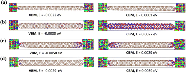
Fig. 5 shows the wavefunctions of (8, m)L configurations. There is no delocalization in the wavefunctions of VBM and CBM over CNT in the case of (8, 1)L, indicating semiconducting system and has lower conductance. This observation also supports the fact that (8, 1)S has metallic behavior while (8, 1)L has semiconducting. Whereas in (8, 2)L, the wavefunctions of CBM is delocalized over the CNT which shows metallic properties. Furthermore, in (8, 3)L and (8, 4)L, no delocalization is observed in the wavefunctions of the electronic states which emphasize their semiconducting characteristics. (For other wavefunctions of the electronic states see Fig. S7–S10 in ESI.†)
We then investigated the chirality- and length-dependent electrical transport properties of chiral (10, m) CNTs, (10, 1), (10, 2), (10, 3), and (10, 4), with slightly larger diameter than the (8, m) CNTs in order to see the effect of the tube diameter. The T(E) profiles of chiral (10, 1)S/L and (10, 4)S/L suggested the metallic transport as shown in Fig. 6a and d, left panel, according the (n − m) rule (see the density of states in Fig. S12 in the ESI†). Well-delocalized transmission eigenchannels confirmed the metallic behavior of the of the (10, 1)S/L and (10, 4)S/L regardless of the length of the tube. Meanwhile, the T(E) values of the (10, 2)S/L and (10, 3)S/L CNTs are negligible at the Ef and the transmission eigenchannels were localized at the left electrode as shown in Fig. 6b and c.
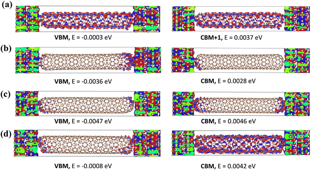
The coupling energy of (10, m)S/L systems i.e. (10, 1)S/L, (10, 2)S/L, (10, 3)S/L, and (10, 4)S/L are shown in Table 1, indicating the (10, 1)S exhibits stronger coupling than other (10, m) systems. Notably, the coupling energy values drop as the nanotube length increases. The wavefunctions of the electronic states near the Ef for chiral (10, m) structures are shown in Fig. 7. The wavefunctions of VBM and CBM + 1 are delocalized over CNT in the case of (10, 1)S, indicating metallic behavior. Whereas in (10, 2)S and (10, 3)S, the wavefunctions of VBM and CBM are not delocalized which depicts semiconducting characteristics. The wavefunctions of CBM are well delocalized over the CNT in (10, 4)S, exhibiting metallic properties. (For other wavefunctions of the electronic states see Fig. S13–S16 in ESI.†)
Fig. 8 depicts the wavefunctions of (10, m)L configurations. There is significant delocalization in wavefunctions of VBM − 1 and CBM + 2 across the CNT in (10, 1)L, which indicates metallic character in the system. In contrast, no such delocalization is observed in the wavefunctions of VBM and CBM for (10, 2)L and (10, 3)L, confirming semiconducting behavior. Furthermore, the (10, 4)L exhibits significant delocalization in the wavefunction of CBM + 3 throughout the CNT which reveals metallic properties. (For other wavefunctions of the electronic states see Fig. S17–S20 in the ESI.†)
Table 1 shows the charge transfer analysis for (10, m)S/L and charge transfer is observed, in all the systems. The charge transfer for (10, 1)S/L are 2.831/0.961 (e). In (10, 2)S/L the charge transfer values are 2.96/0.788 (e). Similarly, the charge transfer values for (10, 3)S/L are 0.963/0.927 (e). While in (10, 4)S/L the charge transfer is 0.946/1.199 (e) respectively. Except (10, 4), there is similar pattern of decreasing charge transfer with increasing the nanotube length of three systems. The charge transfer increases with the coupling energy between the electrode and scattering region except (10, 4)S/L.
As shown in Fig. 9, the I–V curves of the (10, m)S/L CNTs display significant distinction upon the chirality but not upon the length of the tubes. The (10, 1)S/L and (10, 4)S/L exhibited the metallic behavior, while the (10, 2)S/L and (10, 3)S/L exhibited the semiconducting behavior, according to the (n − m) rule. (For the comparison of I–V curves of the shorter and longer CNTs see Fig. S21 in ESI.†) In general, the (10, m) series exhibited larger conductance than the (8, m) series studied here due to a larger tube diameter. Among the (10, m) series, we may suggest the (10, 3) CNT as the optimal choice for a semiconducting molecular junction device with significant conductance.
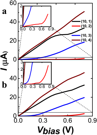 | ||
| Fig. 9 I–V curves values of chiral (10, 1), (10, 2), (10, 3), and (10, 4) as (a) shorter and (b) longer length. Zoom view of (10, 2) as inset in (a) and (b). | ||
4. Conclusion
In conclusion, we investigated the chirality- and length-dependent transport properties of chiral CNTs of (8, m)S/L and (10, m)S/L series using the DFT calculations employing the NEGF formalism. The transmission coefficients T(E), DOS, transmission eigenchannels, coupling energies, and wavefunctions of the electronic demonstrated that the transport properties of these chiral CNT-based devices were significantly influenced by their chirality.Firstly, our studies revealed the remarkable behavior of the (8, m) CNT family. Due to its shorter length, the (8, 1) nanotube was found to have metallic properties which contradicted the (n − m) rule. However, (8, 2), (8, 3) and (8, 4) aligned with the rule, exhibiting metallic and semiconducting properties as expected. Meanwhile, the transport properties of the (10, m) series are consistent with the (n − m) rule.
Secondly, we focused on the length dependent transmission characteristics of (8, m) and (10, m) CNTs. Notably, no significant effect of length was observed on electron transmission except chiral (8, 1)S/L. Near the Ef (8, 1)S shows metallic and (8, 1)L shows semiconducting properties while all other systems had no appreciable impact on transmission by altering the nanotube length.
The coupling energy values shows strong coupling between the electrodes and scattering region and the values decreases with increasing the length. The wavefunction analysis of the electronic states prevails the overlapping between the wavefunctions of gold electrodes and scattering region in all the systems and showing the metallic and semiconducting properties according to (n − m) rule. These outcomes hold a significant implication in the design of small electronic devices, allowing for better performance and usefulness in future technological applications.
Data availability
Data will be made available on request.Conflicts of interest
The authors declared no conflict of interest.Acknowledgements
This work was supported by the National Research Foundation of Korea (NRF) grant funded by the Korea government (MSIT) (no. 2021R1C1C2007977).References
- H. Sugime, S. Esconjauregui, J. W. Yang, L. D’Arsie, R. A. Oliver, S. Bhardwaj, C. Cepek and J. Robertson, Appl. Phys. Lett., 2013, 103, 073116, DOI:10.1063/1.4818619.
- A. C. Torres-Dias, T. F. T. Cerqueira, W. W. Cui, M. A. L. Marques, S. Botti, D. Machon, M. A. Hartmann, Y. W. Sun, D. J. Dunstan and A. San-Miguel, Carbon, 2017, 123, 145–150, DOI:10.1016/j.carbon.2017.07.036.
- K. Gharbavi and H. A. Badehian, Optik, 2016, 127, 3940–3942, DOI:10.1016/j.ijleo.2016.01.110.
- S. Iijima, Nature, 1991, 354, 56–58, DOI:10.1038/354056a0.
- Y. T. Singh, P. K. Patra, N. N. Hieu and D. P. Rai, Surf. Interfaces, 2022, 29, 101815, DOI:10.1016/j.surfin.2022.101815.
- P. Zhao and D. S. Liu, Chin. Sci. Bull., 2010, 55, 4104–4107, DOI:10.1007/s11434-010-4216-y.
- K. M. Alam and S. Pramanik, Adv. Funct. Mater., 2015, 25, 3210–3218, DOI:10.1002/adfm.201500494.
- A. Rochefort, P. Avouris, F. Lesage and D. R. Salahub, Phys. Rev. B: Condens. Matter Mater. Phys., 1999, 60, 13824–13830, DOI:10.1103/PhysRevB.60.13824.
- M. S. Dresselhaus, G. Dresselhaus, J. C. Charlier and E. Hernández, Philos. Trans. R. Soc., A, 2004, 362, 2065–2098, DOI:10.1098/rsta.2004.1430.
- M. B. Nardelli, J. L. Fattebert, D. Orlikowski, C. Roland, Q. Zhao and J. Bernholc, Carbon, 2000, 38, 1703–1711, DOI:10.1016/S0008-6223(99)00291-2.
- B. Natarajan, Compos. Sci. Technol., 2022, 225, 109501, DOI:10.1016/j.compscitech.2022.109501.
- V. Jain, S. Jaiswal, K. Dasgupta and D. Lahiri, Polym. Compos., 2022, 43, 6344–6354, DOI:10.1002/pc.26943.
- A. Graham, G. Duesberg, W. Hoenlein, F. Kreupl, M. Liebau, R. Martin, B. Rajasekharan, W. Pamler, R. Seidel and W. Steinhoegl, Appl. Phys. A, 2005, 80, 1141–1151, DOI:10.1007/s00339-004-3151-7.
- C. Biswas and Y. H. Lee, Adv. Funct. Mater., 2011, 21, 3806–3826, DOI:10.1002/adfm.201101241.
- C. Li, E. T. Thostenson and T. W. Chou, Compos. Sci. Technol., 2008, 68, 1227–1249, DOI:10.1016/j.compscitech.2008.01.006.
- R. N. Malhas, S. G. Marquez and P. K. Khoshouei, Desalin. Water Treat., 2021, 226, 85–94, DOI:10.5004/dwt.2021.27230.
- A. Bianco, K. Kostarelos and M. Prato, Curr. Opin. Chem. Biol., 2005, 9, 674–679, DOI:10.1016/j.cbpa.2005.10.005.
- K. Talukdar and A. K. Mitra, Carbon Nanotubes-Synthesis, Characterization, Applications, 2011, pp. 292–324 Search PubMed.
- K. Tsukagoshi, B. W. Alphenaar and H. Ago, Nature, 1999, 401, 572–574, DOI:10.1038/44108.
- E. Tetik, F. Karadağ, M. Karaaslan and İ. Çömez, Int. Scholarly Res. Not., 2012, 2012, 416417, DOI:10.5402/2012/416417.
- R. Ghasempour and H. Narei, Carbon nanotube-reinforced polymers, Elsevier, 2018, pp. 1–24 Search PubMed.
- L. Malysheva, Low Temp. Phys., 2022, 48, 907–913, DOI:10.1063/10.0014581.
- M. E. Khan, Q. Wali, M. Aamir and Y. H. Kim, Mater. Today Commun., 2022, 32, 104074, DOI:10.1016/j.mtcomm.2022.104074.
- D. Pozdnyakov, V. Galenchik, F. Komarov and V. Borzdov, Phys. E, 2006, 33, 336–342, DOI:10.1016/j.physe.2006.03.158.
- D. V. Pozdnyakov, V. O. Galenchik, V. M. Borzdov and F. F. Komarov, Proc. SPIE, 2006, 6328, 63280Y, DOI:10.1117/12.680528.
- S. U. Lee, R. V. Belosludov, H. Mizuseki and Y. Kawazoe, Small, 2009, 5, 1769–1775, DOI:10.1002/smll.200801938.
- P. Wei, L. L. Sun, E. Benassi, Z. Y. Shen, S. Sanvito and S. M. Hou, J. Chem. Phys., 2011, 134, 244704, DOI:10.1063/1.3603446.
- B. Kang, D. Cho and J. Y. Lee, Phys. Chem. Chem. Phys., 2017, 19, 7919–7922, 10.1039/C7CP00137A.
- S. Meena and S. Choudhary, Mater. Chem. Phys., 2018, 217, 175–181, DOI:10.1016/j.matchemphys.2018.06.077.
- M. Z. Kauser and P. P. Ruden, J. Appl. Phys., 2007, 102, 033712, DOI:10.1063/1.2767224.
- M. Z. Kauser and P. P. Ruden, Appl. Phys. Lett., 2006, 89, 162104, DOI:10.1063/1.2362973.
- J. Liu, J. Lu, X. Lin, Y. Tang, Y. Liu, T. Wang and H. Zhu, Comp. Mater. Sci., 2017, 129, 290–294, DOI:10.1016/j.commatsci.2016.12.035.
- R. Saito, M. Fujita, G. Dresselhaus and U. M. Dresselhaus, Appl. Phys. Lett., 1992, 60, 2204–2206, DOI:10.1063/1.107080.
- B. G. Cook, W. R. French and K. Varga, Appl. Phys. Lett., 2012, 101, 153501, DOI:10.1063/1.4756693.
- P. Zhao, P. J. Wang, Z. Zhang and D. S. Liu, Physica B, 2010, 405, 446–450, DOI:10.1016/j.physb.2009.09.009.
- P. G. Collins and P. Avouris, Sci. Am., 2000, 283, 62–69, DOI:10.1038/scientificamerican1200-62.
- A. Mueller, K. Y. Amsharov and M. Jansen, Fullerenes, Nanotubes Carbon Nanostruct., 2012, 20, 401–404, DOI:10.1080/1536383x.2012.655215.
- W. Su, X. Li, L. Li, D. Yang, F. Wang, X. Wei, W. Zhou, H. Kataura, S. Xie and H. Liu, Nat. Commun., 2023, 14, 1672, DOI:10.1038/s41467-023-37443-7.
- B. Xu, T. Kaneko, Y. Shibuta and T. Kato, Sci. Rep., 2017, 7, 11149, DOI:10.1038/s41598-017-11712-0.
- K. Eklund and A. J. Karttunen, Nanomaterials, 2022, 12, 199, DOI:10.3390/nano12020199.
- J. H. Wu, F. Hagelberg, T. C. Dinadayalane, D. Leszczynska and J. Leszczynski, J. Phys. Chem. C, 2011, 115, 22232–22241, DOI:10.1021/jp207510n.
- M. Ghorbani-Asl, P. D. Bristowe and K. Koziol, Phys. Chem. Chem. Phys., 2015, 17, 18273–18277, 10.1039/c5cp01470k.
- H. Khalfoun, P. Hermet, L. Henrard and S. Latil, Phys. Rev. B: Condens. Matter Mater. Phys., 2010, 81, 193411, DOI:10.1103/PhysRevB.81.193411.
- S. Grimme, C. Bannwarth and P. Shushkov, J. Chem. Theory Comput., 2017, 13, 1989–2009, DOI:10.1021/acs.jctc.7b00118.
- B. Hourahine, B. Aradi, V. Blum, F. Bonafé, A. Buccheri, C. Camacho, C. Cevallos, M. Y. Deshaye, T. Dumitrica, A. Dominguez, S. Ehlert, M. Elstner, T. van der Heide, J. Hermann, S. Irle, J. J. Kranz, C. Köhler, T. Kowalczyk, T. Kubar, I. S. Lee, V. Lutsker, R. J. Maurer, S. K. Min, I. Mitchell, C. Negre, T. A. Niehaus, A. M. N. Niklasson, A. J. Page, A. Pecchia, G. Penazzi, M. P. Persson, J. Rezác, C. G. Sánchez, M. Sternberg, M. Stöhr, F. Stuckenberg, A. Tkatchenko, V. W. Z. Yu and T. Frauenheim, J. Chem. Phys., 2020, 152, 124101, DOI:10.1063/1.5143190.
- J. M. Soler, E. Artacho, J. D. Gale, A. Garcia, J. Junquera, P. Ordejon and D. Sanchez-Portal, J. Phys.: Condens. Matter, 2002, 14, 2745–2779, DOI:10.1088/0953-8984/14/11/302.
- J. P. Perdew, K. Burke and M. Ernzerhof, Phys. Rev. Lett., 1996, 77, 3865–3868, DOI:10.1103/PhysRevLett.78.1396.
- N. Troullier and J. L. Martins, Phys. Rev. B: Condens. Matter Mater. Phys., 1991, 43, 1993–2006, DOI:10.1103/PhysRevB.43.1993.
- Y. Matsuda, J. Tahir-Kheli and W. A. Goddard, J. Phys. Chem. Lett., 2010, 1, 2946–2950, DOI:10.1021/jz100889u.
- S. I. Allec and B. M. Wong, J. Phys. Chem. Lett., 2016, 7, 4340–4345, DOI:10.1021/acs.jpclett.6b02271.
- K. C. Ko, D. Cho and J. Y. Lee, J. Phys. Chem. A, 2012, 116, 6837–6844, DOI:10.1021/jp211225j.
- D. Cho, K. C. Ko, H. Park and J. Y. Lee, J. Phys. Chem. C, 2015, 119, 10109–10115, DOI:10.1021/acs.jpcc.5b01288.
- S. S. Yu, Q. B. Wen, W. T. Zheng and Q. Jiang, Nanotechnology, 2007, 18, 165702, DOI:10.1088/0957-4484/18/16/165702.
- E. Durgun, S. Dag, S. Ciraci and O. Gulseren, J. Phys. Chem. B, 2004, 108, 575–582, DOI:10.1021/jp0358578.
- R. P. Kaur, R. S. Sawhney and D. Engles, Mol. Phys., 2016, 114, 2289–2298, DOI:10.1080/00268976.2016.1197431.
- X. M. Xie, P. H. Li, Y. X. Xu, L. Zhou, Y. H. Yan, L. H. Xie, C. C. Jia and X. F. Guo, ACS Nano, 2022, 16, 3476–3505, DOI:10.1021/acsnano.1c11433.
- Y. H. Zhou, X. H. Zheng, Y. Xu and Z. Y. Zeng, J. Chem. Phys., 2006, 125, 244701, DOI:10.1063/1.2409689.
- Q. Han, B. Cao, L. P. Zhou, G. J. Zhang and Z. H. Liu, J. Phys. Chem. C, 2011, 115, 3447–3452, DOI:10.1021/jp1089917.
Footnote |
| † Electronic supplementary information (ESI) available. See DOI: https://doi.org/10.1039/d3cp05338e |
| This journal is © the Owner Societies 2024 |

