
 Open Access Article
 This Open Access Article is licensed under a
 Creative Commons Attribution 3.0 Unported Licence
Identifying winner-takes-all emergence in random nanowire networks: an inverse problem
F. R.
Duarte
 *a,
S.
Mukim
ab,
M. S.
Ferreira
ab and
C. G.
Rocha
cde
*a,
S.
Mukim
ab,
M. S.
Ferreira
ab and
C. G.
Rocha
cde
aSchool of Physics, Trinity College Dublin, Dublin 2, Ireland. E-mail: duarteff@tcd.ie
bCentre for Research on Adaptive Nanostructures and Nanodevices (CRANN) & Advanced Materials and Bioengineering Research (AMBER) Centre, Trinity College Dublin, Dublin 2, Ireland
cDepartment of Physics and Astronomy, University of Calgary, 2500 University Drive NW, Calgary, Alberta T2N 1N4, Canada
dHotchkiss Brain Institute, University of Calgary, 3330 Hospital Drive NW, Calgary, Alberta T2N 4N1, Canada
eInstitute for Quantum Science and Technology, University of Calgary, Calgary, Alberta, Canada
First published on 12th November 2024
Abstract
Random nanowire networks (NWNs) are interconnects that enable the integration of nanoscopic building blocks (the nanowires) in a disorganized fashion, enabling the study of complex emergent phenomena in nanomaterials and built-in fault-tolerant processing functionalities; the latter can lead to advances in large-scale electronic devices that can be fabricated with no particular array/grid high-precision pattern. However, when various nanowires are assembled to form an intricate network, their individual features are somehow lost in the complex NWN frame, in line with the complexity hallmark “the whole differs from the sum of the parts”. Individual nanowire materials and geometrical features can only be inferred indirectly by attempting to extract information about their initial conditions from a response function measurement. In this work, we present a mathematical framework that enables inference of the intrinsic properties of highly complex/intricate systems such as random NWNs in which information about their individual parts cannot be easily accessed due to their network formation and dynamical conductance behaviour falling in the category of memristive systems. Our method, named misfit minimization, is rooted in nonlinear regression supervised learning approaches in which we find the optimum parameters that minimize a cost function defined as the square least error between conductance evolution curves taken for a target NWN system and multiple configurational NWN samples composing the training set. The optimized parameters are features referent to the target NWN system's initial conditions obtained in an inverse fashion: from the response output function, we extract information about the target system's initial conditions. Accessing the nanowire individual features in a NWN frame, as our methodology allows, enables us to predict the conduction mechanisms of the NWN subjected to a current input source; these can be via a “winner-takes-all” energy-efficient scheme using a single conduction pathway composed of multiple nanowires connected in series or via multiple parallel conduction pathways. Predicting the conduction mechanism of complex and dynamical systems such as memristive NWNs is critical for their use in next-generation memory and brain-inspired technologies since their memory capability relies on the creation of such pathways activated and consolidated by the input current signal.
1 Introduction
Nanowire networks (NWNs) possess exceptional mechanical strength and flexibility,1,2 electrical conductivity,3,4 and catalytic activity5,6 when compared to certain conventional/continuous bulk materials. Randomly dispersed nanowires as depicted in Fig. 1, usually comprised of core metallic nanowires coated with a dielectric layer, exploit such properties to be used as sensors,7,8 memory devices,9,10 thin-film solar cells,11–13 energy storage,14 and transparent conductors,15–20 to name a few. When metallic nanowires are coated with a dielectric material, one can observe the emergence of memristive properties,21–25 which is to say that their electrical conductance depends on the history of the applied bias voltage. Such memristive property is at the heart of the development of brain-like neuromorphic architectures because it reflects an adaptive resistive behaviour similar to the neuronal firing in the human brain. As a result, such memristive systems can be used to inspire the development of novel brain-like hardware or neuromorphic systems.26–32 In other words, when attempting to mimic neuromorphic behaviours, such networks of memristive systems exhibit adaptive activation behaviours in which the conductance of a memristive channel or junction is modulated by the current or charge flowing through it.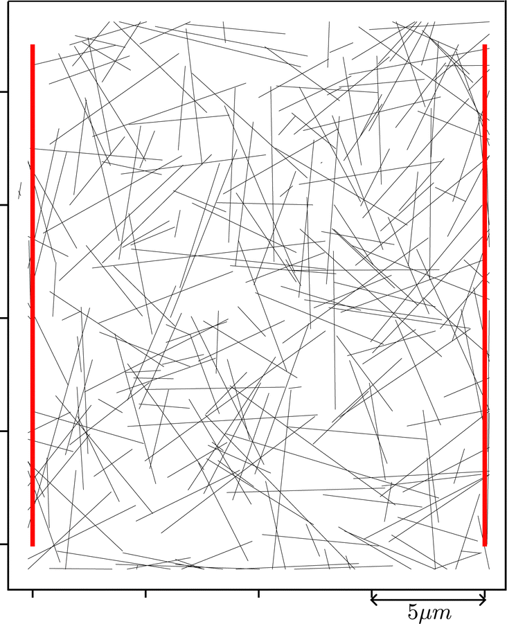 | ||
| Fig. 1 Computationally generated nanowire network geometry with a density of 0.67 nanowires per μm2. The black lines represent the coated metal nanowires (in our case simulated to be Ag/PVP core–shell nanowires). The red vertical lines represent the metallic leads acting as electrodes. The scale bar at the bottom right part of the plot indicates 5 μm in length. | ||
For the case of the NWNs studied here, memristive junctions are organized in a network, they may compete with one another for activation during a linear ramp-up current evolution process; this can lead to a highly selective conducting state in which just a few junctions in the network take the load of propagating most of the current being sourced in the system. As in a mechanism to minimize power dissipation, under specific conditions, this state can evidence a single conducting path formed of nanowires arranged as memristive units in series. This selective conducting strategy aligns with artificial intelligence neuromorphic algorithms such as the “winner-takes-all” (WTA) implemented in computational neural network models, offering an in materia counterpart to the algorithm where the memory states are stored in the variable resistance states of the NWN.30,33–36 The use of adaptive path formation in NWNs for neuromorphic applications has been demonstrated experimentally and described theoretically; Loeffler et al.31 have shown via simulations an analogous to “synaptic metaplasticity” in the brain and the memory capabilities of NWNs when conductance path formation is reinforced in their skeleton; Diaz-Alvarez et al.37 combined experiments and simulations to describe the emergent dynamics and current pathway formation in NWNs using a robust atomic switching model that was able to elucidate prime neuromorphic features such as collective memory response, contrasting ON-OFF resistance states, and fault-tolerant capabilities. In subsequent work, Diaz-Alvarez et al.38 demonstrated an associative memory device out of NWNs by controlling their multiple resistance pathways. Remarkably, Zhu et al.32 took advantage of such NWN path formation dynamics to successfully demonstrate online learning from the NWN spatiotemporal dynamics by subjecting the networks to perform image classification and memory recollection tasks. In a noteworthy review article, Kuncic and Nakayama27 highlight various works that focus on the use of NWNs as neuromorphic hardware, with emphasis on their dynamical interconnectivity pattern of current path formation (including WTA states) and adaptability to time-dependent electrical stimuli relevant to applications in neuromorphic computing.
The WTA connectivity paths formed in NWNs are critical to defining the independently addressable memory or conductance states of the system. The formation of a WTA in a NWN system depends on various factors such as the characteristics of the junctions, the materials composing the core–shell nanowires, the overall network connectivity, and the junction density of the NWN. Because the phenomenon depends on so many correlated factors, conditions, and variables – some of them not directly accessible experimentally – it is key to conduct computational simulations to shed light on the main mechanisms that trigger (or not) WTA states. Manning et al.33 provided experimental confirmation and a modelling framework for WTA conducting pathways in NWNs formed with Ag nanowires coated with polyvinylpyrrolidone (PVP). To experimentally verify that a NWN would form a single WTA path, the authors used passive voltage contrast scanning electron microscopy imaging technique that depicted the wires being ‘short-circuited’ in the WTA path with distinguished colour contrast. This tedious imaging process, however, requires the activation of the system at least up until the formation of the WTA path. It would be useful to predict if a NWN will develop a WTA path or not prior to any excitation and in the absence of sophisticated microscopy imaging methods – as if one could foresee “the future” of the NWN. Moreover, Manning et al.33 performed extensive work on Ag/PVP NWNs which are prone to WTA states, but there is a wide range of core–shell material combinations that can be tested for WTA; a predictive computational method that could anticipate the emergence of WTA, before experimentation and for a wide variety of material specs, would enable the direct correlation of the initial conditions and intrinsic characteristics of the NWNs with its final (potential) WTA state. For that, one needs to rely on an inverse methodology that can decode the final WTA conductance state by inferring the inputs and initial conditions that lead to such a state. This inference is done with minimum information about how the NWNs are initially prepared. In this work, we present an inversion scheme capable of extracting NWN junction parameters that are crucially linked to the formation of WTA as well as parameters that are useful for the overall electrical characterization of the network junctions. We apply a computational inversion method, previously tested in disordered low-dimensional materials,39–42 that was able to estimate the concentration of scattering impurities based solely on the electronic conductance response of the system without any prior knowledge about its composition. The same principle is now adopted to uncover intrinsic properties of systems of higher complexity such as the NWNs. By accessing the NWN conductance response evolution, this method can extract information regarding the intrinsic properties of the system, e.g., the main parameters that rule their memristive junction properties, which, in turn, are associated with the emergence (or not) of WTA-conducting states. Consequently, we are able to provide a robust computational framework that can directly complement experimental microscopy means to characterize NWNs, including their material and overall network features.
To summarize our motivation, this work is guided by the challenges often encountered by computational descriptions when investigating real-world disordered nanomaterials that do not exhibit highly symmetric crystalline structures, impeding for instance, the use of periodicity arguments such as in Bloch's theorem. Amidst this challenge, we offer a computational framework that can infer the a priori unknown intrinsic properties of highly disordered nanomaterials. We introduce a novel supervised learning-based methodology that can extract unknown or inaccessible information out of disordered or amorphous types of materials, such as random NWNs. This will enable the inference or estimation of their intrinsic features theoretically. As demonstrated in Bellew et al.,43 the properties of a single interwire junction can be assessed in a simplified setup of only two nanowires in contact forming a single junction unit. This simplified configuration characterizes a very reduced “sample” out of a “population” of junctions when the nanowires form a network. The single junction experiment certainly provides an initial assessment of a junction, however, this may not characterize the complex environment when many junctions are interlinked in a NWN. Therefore, this research was driven to deliver a framework that can inform experiments conducted in disorder types of nanomaterials in which complexity and emergent effects can play a role in their collective responses. This framework, founded in an optimization scheme of a cost function (the misfit conductance function), can extract the intrinsic characteristics or initial conditions of the nanowires in a network environment and can predict how the NWN will evolve in time, following an inverse modelling fashion explained in detail in this work.
2 Background – the junction power law conductance model
In this section, we will revise the systems in question, i.e., NWNs prone to WTA states and define their main parameters used to model such conducting emergent features. We will also revise the main stages in the time evolution of a NWN subjected to a current ramp-up excitation that may lead to the formation of a WTA state. Fig. 2 shows a circuit representation of a simple NWN motif made of just three nanowires for illustration. Multiple interconnected nanowires can be mapped as a network made of nodes and edges. In this representation, named multi-nodal representation (MNR), the nodes are the contact points on each wire or the nodal voltage points that can be connected by a lumped circuit element. In the case of memristive NWNs, two resistive lumped circuit elements are used to describe their conduction properties: static Ohmic resistors and dynamical memristive units. Nodal voltage points located on the same wire, as shown in the figure, will be connected by an inner “edge” resistor described by the standard law Rin = ρ![[small script l]](https://www.rsc.org/images/entities/char_e146.gif) /Ω with ρ being the resistivity of the core metal, is the length segment between the two voltage nodal points, and Ω is the wire cross-sectional area. These inner resistances are considered static or Ohmic in nature.
/Ω with ρ being the resistivity of the core metal, is the length segment between the two voltage nodal points, and Ω is the wire cross-sectional area. These inner resistances are considered static or Ohmic in nature.
 | ||
| Fig. 2 Schematics of core–shell nanowire contact points depicting the main resistance contributions in our circuit model. Three nanowires made of a metallic core (internal silver cylinders) are coated by a dielectric material (outer blue cylinders) and are in direct contact at two locations: at left and right positions with respect to the bottom nanowire depicted horizontally. At each contact point, two distinct voltage nodes or terminals are created (red spheres). The resistance inside a wire segment (orange resistor symbol) is described by an Ohmic resistance given by Rin = ρ/Ω with ρ being the resistivity of the core metallic material, the length segment between the two voltage nodal points, and Ω the wire cross-sectional area. A resistive junction j used to model the inter-wire dynamic conduction is represented by black resistor symbols and is characterized by a junction resistance Rj which is a function of the parameters Aj and αj defining the phenomenological power law Rj = I−αj/Aj being I the amount of current flowing through the junction. | ||
A pair of nodes in different wires that share the same contact defines a “junction” – the region of contact between two wires, and the point where the memristive properties of the dielectric coating are relevant. These junctions are described by memristive units whose resistance (Rj) changes as a function of the amount of current flowing through them and the history of the voltage applied across them. We can verify experimentally that certain nanomaterial systems whose transport properties are dominated by junctions display self-similarity, which is to observe that each nanowire junction possesses similar power scaling to that of the collective behaviour of the NWN junctions.33,34 Following the model used in our past works, the interwire junction resistance Rj or its reciprocal conductance Γj = 1/Rj can change from a low resistance state (LRS) to a high resistance state (HRS) via an activation process ruled by a phenomenological power law given by Γj = AjIαj in which I is the current flowing through the junction and Aj and αj are power law parameters that characterize the intrinsic properties of the junction. It is worth mentioning that our power law junction model has cut-offs in which the junction resistance cannot be larger than RHRS ∼ 104 kΩ and cannot be smaller than RLRS = 12.9 kΩ which is equivalent to the resistance quantum Rq = h/2e2 with h being the Planck constant and e the elementary charge. These cut-offs were established based on previous experimental results in which 104 kΩ is already a sufficiently high resistance for the kinds of dielectric coatings considered and 12.9 kΩ is based on the assumption that the amount of current compliance set in the experiments is enough to form one single conductance quantum channel inside the junction. The junction power law model with cut-offs as discussed above for fixed αj values and scanned as a function of Aj and I (source current) can be visualized in Fig. 3 as colourmap surfaces. The three panels correspond to the cases in which αj = 1.3 (top panel), αj = 1 (middle panel), and αj = 0.7 (bottom panel). In our previous works,33,34 it was observed that αj fluctuates around 1, therefore, one can view the case of αj = 1 as a critical point. This criticality aspect will be even more evident when we discuss the collective conductance obtained for NWNs (not only a single junction), and we will get back to it in subsequent sections. This figure shows clearly the regions of high and low conductance for a range of Aj at a fixed exponent αj. We can see that when αj < 1, the activation of the junction, i.e., when Γj starts to increase above the cut-off ΓHRS = 1/RHRS, initiates at lower current values but its conductance growth is slower or sublinear. Setting αj ≥ 1 will result in the junction activating at higher currents but its conductance growth will be faster, linear and supralinear, respectively. These features in the single junction model will render complex emergent outcomes when incorporated in a NWN frame and it is key to the realization (or not) of WTA states. In the next section, we will recap how the evolution of a NWN, formed by multiple power law conductance junctions, takes place when subjected to a ramp-up current source. This recap will serve to elucidate the necessity of an inverse modelling scheme. As we will see, the main issue is that the relationship of the single-junction parameters Aj and αj with WTA states in NWNs is not well-defined until the NWN has evolved to a known conductance power law due to the self-similarity observed between single junctions and NWNs.33,34 We will build a computational framework that allows us to predict the types of junctions that compose a NWN, meaning to predict Aj and αj from the NWN equivalent conductance and to anticipate if the NWN will develop a WTA state or not at the very early stages of its evolution, i.e., when the network is still activating and there is no sign of a power law being established.
 | ||
| Fig. 3 Surface colourmaps of the conductance junction model as a function of source current (I) and Aj, the prefactor of the junction power law. The latter is given by Γj = AjIαj with Γj being the conductance of the junction and αj being the exponent. This conductance value is capped by two cut-off values defining a HRS and a LRS that the junction can endure. The resistance of the junction Rj = 1/Γj cannot be larger than RHRS ∼ 104 kΩ and cannot be lower than RLRS = 12.9 kΩ known as the resistance quantum. The three panels show three important junction model cases that one needs to consider to subsequently understand the formation or not of WTA states in NWNs: (a) αj = 1.3 to illustrate junction examples of αj > 1, (b) αj = 1, and (c) αj = 0.7 to illustrate junction examples of αj < 1. | ||
3 Background – the conductance evolution in nanowire networks
Once the single conductance junction model is understood, one can incorporate it into a NWN circuit simulation framework in which it is possible to monitor how the equivalent or collective conductance of the NWN evolves as source current is gradually ramped up in their terminals. Because the NWN is composed of static and dynamical resistors, the latter can adapt to the amount of current flowing through them, its conductance will evolve in a nonlinear manner as a function of the source current. As shown in our previous works,33,34 considering that the NWN starts at an OFF state in which all junction resistances are set at RHRS (or in another common notation, Roff) and the current source starts increasing the current flow in equal ΔI current increments, the NWN will pass over three other characteristic regimes which we named transient growth (TG), power law (PL), and post-power-law (PPL). Depending on the choice of Aj and αj values in the power law conductance junction model, each of these phases can be very distinguishable when analyzing the equivalent conductance of the NWN versus sourced current. This can be seen in Fig. 4 which shows some conductance curve evolution examples for the NWN structure presented in Fig. 1. The computational method used to obtain these curves was widely discussed in our past works in,33,34 but we will recap some of its key features in the next section. One can see that for αj > 1, the conductance evolution starts at a conductance plateau (OFF state), followed by a nonlinear conductance increase (TG) and a short power law (PL) regime, with finally the curve exhibiting some discontinuities in the PPL state. For αj < 1, the NWN conductance evolution curves depict a rather monotonic growth (in log–log scale) in which the TG, PL, and PPL stages are not discernible, at least within the chosen current range. Considering that we only have access to the NWN evolution up to the TG stage, is it possible to devise a computational methodology that can predict the subsequent stages that the NWN will undergo, allowing, therefore, the prediction of the intrinsic junction power law conductance model parameters (Aj,αj) without knowing their values a priori? We argue that such a methodology is possible and it is inspired by supervised machine learning schemes in which an objective (or cost) function devised for the NWN conductance response can be minimized to determine the optimum parameters of the junction power law conductance model, based on a nonlinear regression methodology detailed in the next section.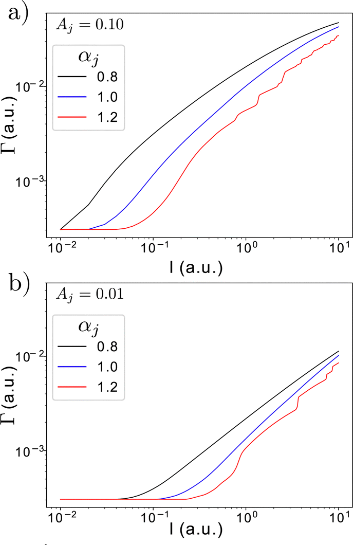 | ||
| Fig. 4 Log–log plots of the NWN conductance evolution as a function of the sourced current; the NWN geometry adopted here is shown in Fig. 1. The junction power law conductance model parameters (given in arbitrary units) used in (a) are for fixed Aj = 0.10 and three distinct curves taken for αj = 0.8,1.0,1.2. In (b), Aj was reduced (and fixed) to Aj = 0.01 and the same αj exponent values as in (a) were used. In all figures, “a.u.” stands for ‘arbitrary units’. | ||
4 Methodology
The inversion methodology is based on the minimization of a cost functional labelled as χ that measures the discrepancy between a desired output response and a set of response averages computed from pre-calculated training sets we build for the system under study. In our case, the output response is the conductance computed for a given NWN (Γ), and the training set, from which conductance averages 〈Γ〉 are also calculated, is built by creating a number Nc of distinct NWN random configurations, each of which possesses one common parameter. This common parameter is the quantity of interest which we aim to characterize from the output response. For each configuration average (CA), this parameter is slightly changed, allowing for a thorough mapping of the parameter space and encoding of the characteristic signatures. For example, one can consider the parameter of interest being αj in which one can build various NWNs with power law junction exponents of αj = 0.7 up to 1.6 varying with equal Δαj increments. The response signal of choice is the NWN conductance evolution with sourced current I such that our target signal with unknown αj value is Γtg(I) and the CAs for each αj value are expressed as with l labelling a NWN configurational sample.
To computationally generate enough network samples so that we could perform the parametric simulations in this work, we extracted the typical wire lengths, nanowire densities, and network sizes from real NWNs synthesized in laboratory and devised a random NWN generation algorithm that would supply us with different synthetic NWNs while keeping essential similarities to the experimental ones. The main nanowire characteristics set in our model are detailed in the Results and Analysis section. A total of Nc = 100 synthetic samples was generated for each parameter characterization. The NWN conductance versus current evolution curves were obtained for all synthetic NWN samples from which the conductance averages taken over all CAs were calculated.
The conductance evolution curves are a result of the NWN memristive-based dynamics formulated in terms of the junction power law model introduced earlier. In this model, all junction conductances in the NWN are not static, rather they vary in accordance with the phenomenological power law model given by  in which (Aj,αj) are parameters that depend on the intrinsic properties of the junction, and In,m is the amount of current flowing between the two terminal nodal points in the junction (n,m). The conductances of the nanowire segments are considered static given by Γin = 1/Rin with Rin being the nanowire inner resistance. We assume the nanowire metal cores are composed of the same material with a fixed inner resistivity of ρ = 22.6 nΩ m (relative to the silver nanowires) and the nanowire diameters fixed at 60 nm.
The NWN conductance evolution simulation starts by setting the initial conditions for all junction resistances at RHRS and considering that a minute amount of current (Imin) is being initially sourced in the metallic electrodes, electrically probing the NWN. Accounting for all NWN connectivity information and Kirchhoff's circuit laws, one can build the conductance matrix ![[M with combining circumflex]](https://www.rsc.org/images/entities/i_char_004d_0302.gif) Γ and apply it to Ohm's law written in matrix form as
Γ and apply it to Ohm's law written in matrix form as
| ΓÛ = Î, | (1) |
Γ and Î, the equation above can be solved for Û which is the potential vector at each voltage node of the network. Once Û is determined at this initial step, we can calculate the equivalent conductance for the whole NWN for the given input current and, moreover, the amount of current (in absolute value) flowing through each junction with terminals labelled (n,m) given by | (2) |
This junction current-flow value is then used to update all junction conductance values using the formula  which will then be re-inserted in Γ for the next evolution step. Note that Γn,m values are bounded by the reciprocal limits [RLRS,RHRS] to emulate the fact that junction conductances cannot increase or decrease indefinitely. The next evolution step is therefore conducted by incrementing the source current by a sufficiently small value of ΔI and repeating the process from equation (1). The NWN conductance evolution is carried on until a predefined maximum current source (Imax) value is reached. How large Imax is will determine if the NWN evolution will cover all transport characteristic regimes as explained earlier named OFF-state, transient growth (TG), power law (PL), and post-power-law (PPL) or just a subset of them. The CAs taken from the built training sets are obtained in such a way that all transport characteristic regimes are evidenced in the NWN conductance evolution.
Now, let us consider a partial conductance evolution curve up to the TG regime from which the NWN (Aj,αj) values are concealed or unknown. This truncated evolution constitutes the target signal of our inversion problem Γtg, and, by obtaining the junction model parameters (Aj,αj) we can infer if the NWN under study is prone to WTA conduction or not. For that, we will describe the χ-minimization scheme devised for the context of memristive NWNs ruled by power law junction models as illustrated above. We start by calculating the CAs which are the averages of the complete conductance evolutions. To infer the power law exponent value, we calculate CAs for the set of networks possessing a systematically varied αj value. In the misfit eqn (3), we calculate the discrepancy between the (truncated) target evolution Γtg of a NWN system and the CAs 〈Γ(I,αj)〉 and integrate within the evolution limits [Imin,Imax] as
 | (3) |
5 Results and analysis
To demonstrate the prediction capabilities and parameter optimization features of the misfit method, we first generate numerous CAs consisting of several NWNs that will evolve in accordance with the power law conductance with cut-offs model described earlier. These constitute our training set from which we know the original parameters (Aj,αj) that result in their conductance evolution curves. In this first analysis, we wish to predict αj from a target conductance curve truncated at a certain maximum current value Imax that does not include the power law regime. For that, we created Nc = 100 NWN conductance evolutions to compose our CAs, each of which set with a fixed Aj = 0.05 and αj values varying from 0.6 up to 1.6 in increments of Δαj = 0.05. It is worth mentioning for the sake of simplicity, we are keeping all model parameters in arbitrary units meaning that conductance and current information are also given in arbitrary units. Realistic physical units can be set with appropriate scaling factors that result in conductances in S (Siemens) and currents in the nA (nanoamperes). We also note that our analysis targets NWN samples set at normal temperature and pressure conditions since this is the case for the experimental samples in Manning et al.33 that inspired this spin-off study. However, it is important to note that temperature and pressure variations can affect the memristive properties of the NWNs. For instance, in a past study, we investigated experimentally and theoretically how the current–voltage hysteresis loops in doped TiO2 memristive nanowires were affected by temperature changes and in air and vacuum conditions.44 That study has shown how the memristive properties of core–shell nanowires can be controlled at distinct temperatures and ambient conditions. We point out that that study was conducted on single nanowires and not on a whole nanowire network and the chosen materials were TiO2-based nanowires. Nonetheless, it already allows us to notice how important thermal and ambient conditions are in memristive systems as also studied by many other groups such as Bae et al.,45 Carapezzi et al.,46 and Kalita et al.47 If required, our computational framework is flexible to accommodate other variational physical factors since the misfit function can be written in terms of any physical quantity set of interest. The main limitation is the inherent computational cost that can become an issue when dealing with multi-dimensional optimization problems. Effective multi-dimensional parameter search techniques or investigating collective distributions of variables as illustrated later in our work can serve as alternatives when computational cost is a limiting factor.The computationally generated NWNs for the CAs resemble realistic NWN samples since their materials and structural features are based on experimental micrograph images from past works.3 While computationally generating the NWNs, the main spatial parameters and constraints set for the pseudo-random generator are:
• Length of electrodes and distance between them; those were set to create squared shape NWNs of 20 × 20 μm.
• The length of nanowires sorted in a given configurational sample is taken from a Gaussian distribution of average length 5.5 μm ± 2 μm standard deviation.
• The total number of nanowires was set to maintain the chosen standard of 900 wire–wire junctions (Nj), representing approximately the average junction density of the observed micrograph images. The number of placed wires also has to guarantee that the electrodes are electrically shortened.
• Each NWN configuration has a unique spatial distribution with nanowires being randomly placed at each generation.
All NWN samples computationally generated per the above recipe were evolved following the conductance evolution model – detailed in the Methodology section – for various αj and Aj values. For each set of (Aj,αj) parameters, the average conductance was computed from all NWN configurational groups for each current stage in the evolution, resulting in various 〈Γ〉 versus current curves. These curves for the whole training set generated are presented in Fig. 5(a) in which we use a colour band representation covering the range of all curves with a given αj value. The dashed and dotted lines on the same plot are the conductance versus current curves for two target NWN systems that we wish to determine their a priori unknown αj values. Note that the conductance evolutions depicted for the target systems only cover up to the TG stage and we do not know if these evolutions will result in αj values greater, equal, or less than 1. For this reason, we apply the misfit minimization scheme to unveil the unknown exponent αj adopted in each target simulation. Using the training set curves to compute the conductance averages plus the target conductance curves into eqn (3), we obtain the log(χ) as a function of αj curves appearing in Fig. 5(b). The current limits of integration used in eqn (3) are consistent with including only the OFF and the TG regimes in the χ cost function. Note that χ as a function of αj curves evidence clear minima. The dashed curve shows a minimum at αmin = 1.1, agreeing with the exponent of the target conductance curve that significantly overlaps with the yellow/green bands in Fig. 5(a). Similarly, the dash-dotted curve shows a minimum at αmin = 0.9, while overlapping with the saffron/orange bands. Another interpretation for the misfit minimization is that χ tracks the mean squared error between the target conductance and various average conductance curves created as the training set for distinct αj values. The ensemble in the training set that minimizes this error reveals the exponent of the target system.
 | ||
| Fig. 5 (a) Colour band representation depicting the collection of average conductance versus current curves generated for the training set used in the misfit minimization scheme. Each collection refers to an ensemble of Nc = 100 synthetic NWN samples evolved using the junction power-law conductance model with cut-offs with Aj = 0.05 and distinct αj values ranging from 0.7 up to 1.6 represented by the depicted colour code. The colour bands populate the region between two consecutive ensemble average curves for given αj values. The dashed and dotted lines are target conductance evolution curves taken for different NWNs evolved up to the TG stage. We do not know a priori their αj exponent. (b) log(χ) versus αj curve computed using eqn (3) to determine each curve minimum. The dashed curve on panel (a) results in the black dashed log(χ) curve with its minimum at αmin = 1.1, while the dotted curve on panel (a) results in the dash-dotted red line showing a minimum at αmin = 0.9. In both cases, the correct exponent used in each target conductance curve was captured by the minimum value, even though that did not reach the power law regime in the evolution. | ||
We repeated the same χ calculation for other concealed αj = 1.1 NWNs as targets to make sure the αj prediction is not impacted by different networks of other spatial/configurational characteristics. For this, we considered a distribution of χ values computed from Ntg = 60 samples, where Ntg is the number of different target NWNs sharing the same αj used to define misfit function distributions (mean and standard deviation). In this way, we can analyze how χ fluctuates with respect to changes in the NWN spatial configuration as shown in Fig. 6. Once more, we can see the presence of a well-defined minimum with reasonable error bars depicting the χ fluctuations. This second identification of a minimum in χ characterizes an inversion calculation scheme; from the output response function of the system, in this case, the conductance as a function of current, one can predict an intrinsic parameter or initial condition of the system. Here, the exponent αj = 1.1, an intrinsic parameter in the conductance power law with cut-offs model, gives the minimum of χ, coinciding with the concealed target value. This is a supralinear exponent (αj > 1), as a result, one can expect the formation of a WTA even though the target function did not reach the power law stage yet. To verify this, one needs to explicitly visualize current pathways, i.e., to visualize how the NWN is distributing the source current through its network structure. This can be done through current colour mapping plots as in Fig. 7. In the figure, nanowire segments carrying substantial amounts of current are depicted in brighter colours. Each current colour mapping depicts a state of the NWN in the evolution curve of Γ versus I; for the results in Fig. 7, we fixed I = 0.25 (arbitrary units) which corresponds to a relatively early stage in the evolution as shown in Fig. 5(a). To demonstrate the contrast between a WTA and a non-WTA (multiple paths) situation, we obtained current maps for αj = 0.9, αj = 1, and αj = 1.1 for a NWN of fixed spatial structure as depicted in Fig. 7(a). In the cases of αj ≤ 1, we observe various nanowire segments being accentuated, indicating that the current sourced in the electrodes is being distributed to distinct sections of the NWN. For αj > 1 however, a single current pathway is highlighted characterizing the WTA state, which the misfit method could correctly predict without the need for current visualization maps.
 | ||
| Fig. 6 Average misfit function χ plotted as a function of exponent αj, developing a minimum at αmin = 1.1, corresponding to the actual value of the target system. The current limits of integration considered in the calculation of χ for the inversion are Imin = 0 to Imax = 0.2 (arbitrary units) and fixed Aj = 0.05 (arbitrary units). The error bars correspond to the standard deviation in χ computed over a NWN target ensemble of Ntg = 60 samples. | ||
 | ||
| Fig. 7 (a) The same NWN as in Fig. 1 but only the nanowire segments that can carry current or are electrically activated are shown. This means that isolated nanowires or nanowire ‘dead ends’ are not depicted. (b)–(d) Current maps obtained at the conductance state at I = 0.25 which corresponds to a state at the transient growth (TG) regime (see Fig. 5(a)). The power law prefactor was fixed at Aj = 0.05. Each panel shows the current color map for a given αj value: (b) αj = 0.9, (c) αj = 1.0, and (d) αj = 1.1. In the panels, α ≡ αj. αj > 1 evidences a WTA scenario whereas in the cases where αj ≤ 1, a multiple path scenario is seen. | ||
Despite the fact that we emphasize the formation of WTA paths in random NWNs, it is important to note that depending on the characteristics of the junctions, WTAs may not develop as depicted in panels 7(b) and 7(c). WTAs are very interesting because they can be viewed as somehow counterintuitive considering the immense number of possible parallel paths a random NWN may have at its disposal to propagate current. Nonetheless, WTAs mostly form when the exponential characteristics of the junctions are supralinear, i.e., αj > 1. When the latter is not fulfilled, our simulations show a multi-path configuration as indicated in the current maps in 7(b) and 7(c). These states are also interesting to study since they are more representative of the emergent properties of the NWNs. In other words, while a WTA path is composed of a number of resistors in series, meaning that most of the equivalent resistance contribution comes from the summation  with Ri being the resistance of the ith resistor in the WTA path and NWTA the number of resistors in the path, a multi-path configuration is not simply the sum of independent resistors, meaning that many junction resistances are evolving in a more collective/interactive environment. During the WTA evolution, some junctions evolve rather rapidly due to their supralinear exponent and local connectivity, whereas in the multi-path state, junctions evolve more collectively, as a result, our framework may be even more critical to characterize multi-path NWNs than WTAs in a complexity science point of view.
It is important to note that the misfit inversion procedure is not limited to infer only the exponent parameter αj. The conductance evolution of a NWN subjected to a current source depends on numerous other parameters such as its connectivity pattern (e.g., wire density that can define how sparse or dense a NWN is), junction density, material resistivity, nanowire length, etc. The procedure can be adapted to infer other variables as well, as we will show for the case of the power law prefactor Aj. Eqn (3) can be rewritten in terms of Aj as the parameter to be inferred from the minimization scheme, i.e., χ is a function of Aj instead. Another way is to conduct a two-dimensional scheme in which the minimization is done in terms of both parameters Aj and αj as we extended in.42 This bi-parametric inversion requires the creation of NWN CAs in a two-dimensional phase space of αj × Aj in which the computed χ points can be depicted as a surface contour plot. We sweep this space with Nc = 100 CAs having Aj values ranging from 0.03 to 0.09 and αj values ranging from 0.6 to 1.6 and applied the multivariable version of eqn (3) to calculate χ. The result is shown in Fig. 8, evidencing a log(χ) minimum at (αj = 1.1, Aj = 0.05), matching the power law model specifications of the target NWN system. Slicing this surface at αj = 1.1, we can visualize the minimum of χ as a function of Aj with clarity at Aj = 0.05 as shown in Fig. 9. In the latter, the χ values are averages taken over Ntg = 60 different target NWN inversions from which we also computed the standard deviations shown as error bars in the plot.
 | ||
| Fig. 8 Surface contour plot of the (logarithm) misfit function in terms of α ≡ αj and Aj taken for a NWN with Nj = 900. The crossing of the horizontal and vertical dashed lines indicates the minimum of the log(χ) surface, matching the parameters initially set for the target NWN system which were αj = 1.1 and Aj = 0.05. | ||
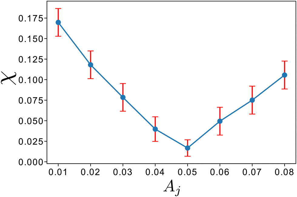 | ||
| Fig. 9 Fixing αj = 1.1 in Fig. 8, one can visualize the misfit function (average) plotted in terms of Aj; the minimum is located at Amin = 0.05, corresponding to the original prefactor set in the target NWN system. The average of χ was computed for Ntg = 60 different target NWNs with an accuracy of 95% and standard deviations shown as error bars. | ||
Having established the efficacy of the inversion method in characterizing the exponent and the power law prefactor modelling nanowire junctions in NWNs, we can construct a more realistic NWN case to test the misfit inversion scheme by considering that the NWN is made of two types of junctions modelled as: (1) Γ1j = A1jIα1j and (2) Γ2j = A2jIα2j. To focus this analysis on the exponents as a first approximation, we will keep A1j ≡ A2j and α1j ≠ α2j with α1j and α2j in the sublinear and supralinear regimes, respectively. This modelling consideration accounts for the fact that some junctions may activate faster (higher exponents) than others due to various microscopic factors, e.g., differences in the ionic mobilities of the charge carriers inside the junctions, differences in sizes of the nanowire coating layers, to name but a few. Fig. 10 shows the misfit function result to identify these two parameters from a target NWN with α1j ≡ α1 = 0.9 and α2j ≡ α2 = 1.2. Note the presence of the two equivalent minima – they arise because there is no differentiation between the indexes of α1 and α2 from the point of view of the calculation. In this case, both configurations of α1 = 0.9 and α2 = 1.2 and α1 = 1.2 and α2 = 0.9 are equiprobable.
 | ||
Fig. 10 Surface contour plot of the (logarithm) misfit function in terms of α1j ≡ α1 and α2j ≡ α2 for a NWN with Nj = 900 and A1j = A2j = 0.05. In this case, the power law exponents for each junction in the NWN target case were randomly assigned to α1 = 0.9 and α2 = 1.2. The proportion of the number of α1 and α2 types of junctions are kept 1![[thin space (1/6-em)]](https://www.rsc.org/images/entities/char_2009.gif) :1. Note that now, since the misfit function cannot differentiate between the variables, this graph will be symmetric along the identity line α1 = α2 (save some oscillations from the stochastic ensemble calculations). This implies that we have two possible minima, one at α1 = 0.9 and α2 = 1.2 and the symmetric one at α1 = 1.2 and α2 = 0.9. :1. Note that now, since the misfit function cannot differentiate between the variables, this graph will be symmetric along the identity line α1 = α2 (save some oscillations from the stochastic ensemble calculations). This implies that we have two possible minima, one at α1 = 0.9 and α2 = 1.2 and the symmetric one at α1 = 1.2 and α2 = 0.9. | ||
The bimodal calculation above can be expanded to consider more than two exponents in the power law model, increasing the complexity of the NWNs, but as the phase space dimensionality of the problem increases, the computational cost for the misfit procedure (and the requirement for more datasets) also increases. Nonetheless, the misfit inversion procedure can be adapted to predict not all the individual αj's considered in the model, but the main parameters characterizing their probability distribution functions used to assign all αj's for all junctions. For instance, let's consider that the NWN target system is now built with a diverse set of junctions in which each αj value is randomly assigned following a Gaussian distribution of mean αμ and standard deviation ασ. These quantities are a priori unknown. We also construct NWN CAs in terms of the Gaussian distribution parameters that will be used in the minimization of the misfit function in eqn (3) written in terms of αμ and ασ. Fig. 11 shows a log(χ) surface as a function of αμ and ασ for a NWN ensemble of Nc = 300 and number of junctions Nj = 900. Once more, the dashed lines crossing marks the minimum in log(χ) found at αminμ = 1.2 and αminσ = 0.2. This last example demonstrates that the misfit minimization method can effectively predict parametric distribution features that characterize more complex NWNs with a wide variety of junction characteristics and material properties within the same NWN structure. In other words, this parametric distribution feature analysis allows the investigation of NWNs that are not as idealized as the first examples studied in this manuscript with all nanowire junctions with the same exponent and prefactor values, enabling hence the inference of more realistic settings as many NWN intrinsic properties and initial conditions can fluctuate significantly from sample to sample.
 | ||
| Fig. 11 Surface contour plot of the (logarithm) misfit function in terms of αμ and ασ taken for a NWN with Nj = 900. In this case, the power law exponents for each junction in the NWN case were randomly assigned following a Gaussian distribution of mean αμ and standard deviation ασ. The crossing of the horizontal and vertical dashed lines indicates the minimum of the log(χ) surface, matching the Gaussian parameters initially set for the target NWN system which were αμ = 1.2 and ασ = 0.2. | ||
6 Conclusions
The results presented in this work offer a solution for the challenging problem of characterizing complex systems such as random NWNs with memristive properties in which their interwire junction resistances can change in response to the history of the input source current. From equivalent conductance versus current curves, we presented a minimization methodology rooted in nonlinear regression supervised learning methods named the misfit minimization in which we can write a cost function in terms of the conductance of the target system, from which we wish to unveil intrinsic (unknown) parameters, and average conductances taken from numerous NWN configurational averages composing of our training dataset. One of the challenges this methodology can address is the fact that the main intrinsic features of random NWNs are often not directly accessible, i.e., we cannot infer the features of a single interwire junction amidst the whole intricate interconnect or spaghetti-like structure that random NWNs characteristically have. We applied the misfit minimization methodology in the context of random NWNs being described by a phenomenological model that considers that the conductance of each interwire junction (Γj) varies in accordance with a current (I) power law function given by Γj = AjIαj, in which the prefactor Aj and exponent αj are intrinsic to the junction and are unknown a priori. The misfit minimization method is capable of inferring these parametric features from the target conductance curve and the average conductance curves from the created dataset, integrated over the very early stages of the NWN being electrically activated by a ramp-up input current, meaning we do not need to store or know much about the history evolution of the NWN to discover its intrinsic initial parameters. Moreover, from the measured/output conductance data curves measured/calculated for the whole NWN, we can determine the optimum Aj and αj parameters that minimize the misfit cost function, meaning the method works in an inversion fashion: from the output information, we infer on the initial conditions of the target system.The prediction of αj, in particular, is very important in the context of memristive NWNs because that gives information on the conduction strategy the NWN is prone to use: it may use a single current pathway to propagate nearly 100% of the sourced current if αj > 1 or it may spread the sourced current into multiple paths if αj ≤ 1. The former is identified as the “winner-takes-all” (WTA) conduction state found in certain core–shell random NWNs studied in our group in the past.33 The misfit function methodology presented here is capable of predicting which exponent a target NWN system will evolve to by only using information from its early activation stages as if the NWN “future” can be anticipated from data acquired way before the NWN reaches the power law regime, being that the training set for the method. We also demonstrated that the methodology can be extended to make parametric predictions in two-dimensional phase space and can infer features of probability density functions that can model collective aspects of the NWNs in distribution form. As the dimensionality of the parametric phase space enhances, the computational cost associated with the methodology also increases, however, the misfit characterization of probability density functions offers a way to balance the computational cost by inferring collective features packed in probability density functions rather than all individual (distinct) variables characterizing, for instance, hundreds of interwire junctions. It is worth mentioning that the orders of magnitude of all parameters (floating or fixed) studied in this work are within the experimental range of NWN samples as studied in Manning et al.33 which were made of core–shell silver-PVP nanowires. We worked to fit exponents that are within the range of their findings, i.e., αj ≈ 1, prefactors Aj ∼ 0.1 (in arbitrary units), current sweeps in the nanoampere range, silver resistivity chosen from past experimental results at ρ ≈ 22 nΩ m, conductances in the range of the conductance quantum when they are activated (ON state) and in the hundreds of Ohms when deactivated (OFF state), and NWN sizes within experimental range of 20 × 20 μm. In this way, we managed to constrain the optimizations conducted in this work within experimental acceptable values.
This work demonstrates that the misfit minimization method can be applied to make key predictions in highly complex/disordered systems such as random NWNs exhibiting dynamical memristive behaviour, standing as a powerful mathematical tool for materials characterization when detailed microscopy experimental methods are not available or the initial conditions of the system under study, that responded to a certain input stimulus, are unknown. This strategy can be crucial when designing NWNs to meet certain adaptive conduction target functions that can serve future neuromorphic technologies.
Author contributions
FRD, SM, and CGR took part in the modelling and calculations (data curation, analysis, software, visualization). MSF and CGR lead the research (funding acquisition, project administration, supervision). All authors took part in the research (conceptualization, investigation, methodology, validation) and co-wrote the paper (writing).Data availability
The data generation scripts through which one can reproduce the findings presented in this article are available in the GitHub repository at https://github.com/mukims/WTA_ANINVERSEPROBLEM.Conflicts of interest
There are no conflicts to declare.Acknowledgements
This publication has emanated from research supported partly by a research grant from Taighde Éireann (former SFI) under grant no. SFI12RC2278_P2. FRD wishes to acknowledge the Trinity Centre for High Performance Computing (Research IT) for the provision of computational facilities and support. CGR would like to acknowledge UofC start-up funding, the Natural Sciences and Engineering Research Council of Canada (NSERC) – Discovery Grant, the Quantum City initiative, and the NSERC Alliance - Alberta Innovates – Advance Program (Stream I) for the support. CGR also acknowledges the Advanced Research Computing (ARC) facilities at the UofC, the specialized UofC Customer Technology Services team with T. MacRae and B. Michaels, the Digital Research Alliance of Canada (former Compute Canada), and the CMC Microsystems for computational resources.References
- H. Sohn, C. Park, J. M. Oh, S. W. Kang and M. J. Kim, Silver nanowire networks: Mechano-electric properties and applications, Materials, 2019, 12(16), 2526 CrossRef CAS PubMed.
- S. Imtiaz, I. S. Amiinu, D. Storan, N. Kapuria, H. Geaney and T. Kennedy, et al., Dense Silicon Nanowire Networks Grown on a Stainless-Steel Fiber Cloth: A Flexible and Robust Anode for Lithium-Ion Batteries, Adv. Mater., 2021, 33(52), 2105917 CrossRef CAS PubMed.
- C. G. Rocha, H. G. Manning, C. O’Callaghan, C. Ritter, A. T. Bellew and J. J. Boland, et al., Ultimate conductivity performance in metallic nanowire networks, Nanoscale, 2015, 7(30), 13011–13016 RSC.
- Q. Huang and Y. Zhu, Patterning of metal nanowire networks:methods and applications, ACS Appl. Mater. Interfaces, 2021, 13(51), 60736–60762 CrossRef CAS PubMed.
- M. Chirea, A. Freitas, B. S. Vasile, C. Ghitulica, C. M. Pereira and F. Silva, Gold nanowire networks: synthesis, characterization, and catalytic activity, Langmuir, 2011, 27(7), 3906–3913 CrossRef CAS PubMed.
- N. Ulrich, M. Schäfer, M. Romer, S. D. Straub, S. Zhang and J. Brötz, et al., Cu nanowire networks with well-defined geometrical parameters for catalytic electrochemical CO2 reduction, ACS Appl. Nano Mater., 2023, 6(6), 4190–4200 CrossRef CAS.
- I. Paulowicz, V. Hrkac, S. Kaps, V. Cretu, O. Lupan and T. Braniste, et al., Three-Dimensional SnO2 Nanowire Networks for Multifunctional Applications: From High-Temperature Stretchable Ceramics to Ultraresponsive Sensors, Adv. Electron. Mater., 2015, 1(8), 1500081 CrossRef.
- D. L. Wen, P. Huang, B. Y. Li, Y. Qiu, Y. L. Wang and X. R. Zhang, et al., Silk fibroin/Ag nanowire-based multifunctional sensor for wearable self-powered wireless multi-sensing microsystems, Nano Energy, 2023, 113, 108569 CrossRef CAS.
- A. T. Bellew, A. P. Bell, E. K. McCarthy, J. A. Fairfield and J. J. Boland, Programmability of nanowire networks, Nanoscale, 2014, 6(16), 9632–9639 RSC.
- R. Fang, W. Zhang, K. Ren, P. Zhang, X. Xu and Z. Wang, et al., Inmaterio reservoir computing based on nanowire networks:Fundamental, progress, and perspective, Mater. Futures, 2023, 19(2), 022701 CrossRef.
- J. Liu, D. Jia, J. M. Gardner, E. M. J. Johansson and X. Zhang, Metal nanowire networks: Recent advances and challenges for new generation photovoltaics, Materi. Today Energy, 2019, 13, 152–185 CrossRef.
- K. Chen, B. Zhao, L. Wu, T. Hu, Y. Xiang and T. Chen, et al., Silver nanowire networks on textured silicon as low-emissivity coatings for photovoltaic/thermal applications, Sol. Energy, 2024, 267, 112253 CrossRef CAS.
- H. Lu, J. Lin, N. Wu, S. Nie, Q. Luo and C. Q. Ma, et al., Inkjet printed silver nanowire network as top electrode for semitransparent organic photovoltaic devices, Appl. Phys. Lett., 2015, 106(9), 0003–6951 CrossRef.
- G. Zhou, L. Xu, G. Hu, L. Mai and Y. Cui, Nanowires for electrochemical energy storage, Chem. Rev., 2019, 119(20), 11042–11109 CrossRef CAS PubMed.
- D. Tan, C. Jiang, Q. Li, S. Bi and J. Song, Silver nanowire networks with preparations and applications: a review, J. Mater. Sci.: Mater. Electron., 2020, 31, 15669–15696 CrossRef CAS.
- D. Langley, G. Giusti, C. Mayousse, C. Celle, D. Bellet and J. P. Simonato, Flexible transparent conductive materials based on silver nanowire networks: a review, Nanotechnology, 2013, 24(45), 452001 CrossRef PubMed.
- H. Du, T. Wan, B. Qu, F. Cao, Q. Lin and N. Chen, et al., Engineering silver nanowire networks: from transparent electrodes to resistive switching devices, ACS Appl. Mater. Interfaces, 2017, 9(24), 20762–20770 CrossRef CAS.
- J. Kim, M. Kim, H. Jung, J. Park and Y. Lee, Ultrastable 2D materialwrapped copper nanowires for high-performance flexible and transparent energy devices, Nano Energy, 2023, 106, 108067 CrossRef CAS.
- K. Esteki, D. Curic, H. G. Manning, E. Sheerin, M. S. Ferreira and J. J. Boland, et al., Thermo-electro-optical properties of seamless metallic nanowire networks for transparent conductor applications, Nanoscale, 2023, 15(24), 10394–10411 RSC.
- K. Esteki, H. G. Manning, E. Sheerin, M. S. Ferreira, J. J. Boland and C. G. Rocha, Tuning the electro-optical properties of nanowire networks, Nanoscale, 2021, 13(36), 15369–15379 RSC.
- P. N. Nirmalraj, A. T. Bellew, A. P. Bell, J. A. Fairfield, E. K. McCarthy and C. O’Kelly, et al., Manipulating connectivity and electrical conductivity in metallic nanowire networks, Nano Lett., 2012, 12(11), 5966–5971 CrossRef CAS PubMed.
- D. S. Jeong, R. Thomas, R. S. Katiyar, J. F. Scott, H. Kohlstedt and A. Petraru, et al., Emerging memories: resistive switching mechanisms and current status, Rep. Prog. Phys., 2012, 75(7), 076502 CrossRef PubMed.
- G. Milano, S. Porro, I. Valov and C. Ricciardi, Recent developments and perspectives for memristive devices based on metal oxide nanowires, Adv. Electron. Mater., 2019, 5(9), 1800909 CrossRef.
- J. Resende, A. Sekkat, V. H. Nguyen, T. Chatin, C. Jiménez and M. Burriel, et al., Planar and transparent memristive devices based on titanium oxide coated silver nanowire networks with tunable switching voltage, Small, 2021, 17(21), 2007344 CrossRef CAS PubMed.
- L. A. Moisés and A. J. Chiquito, Enhancing the memristive effects in SnO2 nanowire networks, Curr. Appl. Phys., 2023, 53, 165–171 CrossRef.
- D. V. Christensen, R. Dittmann, B. Linares-Barranco, A. Sebastian, M. Le Gallo and A. Redaelli, et al., 2022 roadmap on neuromorphic computing and engineering, Neuromorphic Comput. Eng., 2022, 2(2), 022501 CrossRef.
- Z. Kuncic and T. Nakayama, Neuromorphic nanowire networks: principles, progress and future prospects for neuroinspired information processing, Adv. Phys.: X, 2021, 6(1), 1894234, DOI:10.1080/23746149.2021.1894234.
- Z. Kuncic, O. Kavehei, R. Zhu, A. Loeffler, K. Fu and J. Hochstetter, et al. Neuromorphic information processing with nanowire networks. In: 2020 IEEE International Symposium on Circuits and Systems (ISCAS). IEEE; 2020. p. 1-5.
- K. Fu, R. Zhu, A. Loeffler, J. Hochstetter, A. Diaz-Alvarez and A. Stieg, et al. Reservoir computing with neuromemristive nanowirenetworks. In: 2020 International Joint Conference on Neural Networks (IJCNN). IEEE; 2020. p. 1-8.
- G. Milano, G. Pedretti, K. Montano, S. Ricci, S. Hashemkhani and L. Boarino, et al., In materia reservoir computing with a fully memristive architecture based on self-organizing nanowire networks, Nat. Mater., 2022, 21(2), 195–202 CrossRef CAS PubMed.
- A. Loeffler, A. Diaz-Alvarez, R. Zhu, N. Ganesh, J. M. Shine and T. Nakayama, et al., Neuromorphic learning, working memory, and metaplasticity in nanowire networks, Sci. Adv., 2023, 9(16), eadg3289 CrossRef PubMed.
- R. Zhu, S. Lilak, A. Loeffler, J. Lizier, A. Stieg and J. Gimzewski, et al., Online dynamical learning and sequence memory with neuromorphic nanowire networks, Nat. Commun., 2023, 14(1), 6697 CrossRef CAS PubMed.
- H. G. Manning, F. Niosi, C. G. Rocha, A. T. Bellew, C. O’Callaghan and S. Biswas, et al., Emergence of winner-takes-all connectivity paths in random nanowire networks, Nat. Commun., 2018, 9(1), 3219 CrossRef PubMed.
- C. O’Callaghan, C. G. Rocha, F. Niosi, H. G. Manning, J. J. Boland and M. S. Ferreira, Collective capacitive and memristive responses in random nanowire networks: Emergence of critical connectivity pathways, J. Appl. Phys., 2018, 124(15), 0021–8979 CrossRef.
- J. J. Wang, Q. Yu, S. G. Hu, Y. Liu, R. Guo and T. P. Chen, et al., Winnertakes-all mechanism realized by memristive neural network, Appl. Phys. Lett., 2019, 115(24), 0003–6951 Search PubMed.
- Q. Li, A. Diaz-Alvarez, R. Iguchi, J. Hochstetter, A. Loeffler and R. Zhu, et al., Dynamic electrical pathway tuning in neuromorphic nanowire networks, Adv. Funct. Mater., 2020, 30(43), 2003679 CrossRef CAS.
- A. Diaz-Alvarez, R. Higuchi, P. Sanz-Leon, I. Marcus, Y. Shingaya and A. Z. Stieg, et al., Emergent dynamics of neuromorphic nanowire networks, Sci. Rep., 2019, 9, 14920 CrossRef.
- A. Diaz-Alvarez, R. Higuchi, Q. Li, Y. Shingaya and T. Nakayama, Associative routing through neuromorphic nanowire networks, AIP Adv., 2020, 10, 025134 CrossRef.
- S. Mukim, F. P. Amorim, A. R. Rocha, R. B. Muniz, C. Lewenkopf and M. S. Ferreira, Disorder information from conductance: a quantum inverse problem, Phys. Rev. B, 2020, 102(7), 075409 CrossRef CAS.
- F. R. Duarte, S. Mukim, A. Molina-Sánchez, T. G. Rappoport and M. S. Ferreira, Decoding the DC and optical conductivities of disordered MoS2 films: an inverse problem, New J. Phys., 2021, 23(7), 073035 CrossRef CAS.
- S. Mukim, C. Lewenkopf and M. S. Ferreira, Spatial mapping of disordered 2D systems: The conductance Sudoku, Carbon, 2022, 188, 360–366 CrossRef CAS.
- S. Mukim, J. O’Brien, M. Abarashi, M. S. Ferreira and C. G. Rocha, Decoding the conductance of disordered nanostructures: a quantum inverse problem, J. Phys.: Condens. Matter, 2021, 34(8), 085901 CrossRef.
- A. T. Bellew, H. G. Manning, C. G. Rocha, M. S. Ferreira and J. J. Boland, Resistance of Single Ag Nanowire Junctions and Their Role in the Conductivity of Nanowire Networks, ACS Nano, 2015, 9, 11422 CrossRef CAS PubMed.
- S. Alialy, K. Esteki, M. S. Ferreira, J. J. Boland and C. G. Rocha, Nonlinear ion drift-diffusion memristance description of TiO2 RRAM devices, Nanoscale Adv., 2020, 2, 2514–2524 RSC.
- S. H. Bae, S. Lee, H. Koo, L. Lin, B. H. Jo and C. Park, et al., The Memristive Properties of a Single VO2 Nanowire with Switching Controlled by Self-Heating, Adv. Mater., 2013, 25, 5098–5103 CrossRef CAS.
- S. Carapezzi, C. Delacour, A. Plews, A. Nejim, S. Karg and A. Todri-Sanial, Role of ambient temperature in modulation of behavior of vanadium dioxide volatile memristors and oscillators for neuromorphic applications, Sci. Rep., 2022, 12, 19377 CrossRef CAS.
- A. J. Kalita, M. Sharma, H. Das and P. K. Kalita, Memristive behaviour of Al/rGO-CdS/FTO device at different temperatures: A MATLAB-integrated study, Phys. E, 2025, 165, 116107 CrossRef CAS.
| This journal is © the Owner Societies 2024 |