
 Open Access Article
 This Open Access Article is licensed under a
 Creative Commons Attribution 3.0 Unported Licence
Fully printed flexible perovskite solar modules with improved energy alignment by tin oxide surface modification†
Lirong
Dong
 a,
Shudi
Qiu
a,
José
García Cerrillo
a,
Michael
Wagner
b,
Olga
Kasian
abc,
Sarmad
Feroze
a,
Dongju
Jang
a,
Chaohui
Li
a,
Vincent
M. Le Corre
ab,
Kaicheng
Zhang
a,
Heiko
Peisert
d,
Felix
U. Kosasih
e,
Caterina
Ducati
e,
Charline
Arrive
f,
Tian
Du
*ab,
Fu
Yang
ag,
Christoph
J. Brabec
*ab and
Hans-Joachim
Egelhaaf
ab
a,
Shudi
Qiu
a,
José
García Cerrillo
a,
Michael
Wagner
b,
Olga
Kasian
abc,
Sarmad
Feroze
a,
Dongju
Jang
a,
Chaohui
Li
a,
Vincent
M. Le Corre
ab,
Kaicheng
Zhang
a,
Heiko
Peisert
d,
Felix
U. Kosasih
e,
Caterina
Ducati
e,
Charline
Arrive
f,
Tian
Du
*ab,
Fu
Yang
ag,
Christoph
J. Brabec
*ab and
Hans-Joachim
Egelhaaf
ab
aInstitute of Materials for Electronics and Energy Technology (i-MEET), Friedrich-Alexander-Universität Erlangen-Nürnberg, Martensstraße 7, 91058 Erlangen, Germany. E-mail: tian.du@fau.de; christoph.brabec@fau.de; lirong.dong@fau.de
bHelmholtz Institute Erlangen-Nürnberg for Renewable Energy (HI ERN), Cauerstraße 1, 91058 Erlangen, Germany
cHelmholtz Zentrum Berlin GmbH, Hahn-Meitner-Platz 1, 14109 Berlin, Germany
dInstitut für Physikalische und Theoretische Chemie, Universität Tübingen, Auf der Morgenstelle 18, Tübingen, Germany
eDepartment of Materials Science and Metallurgy, University of Cambridge, 27 Charles Babbage Road, Cambridge CB3 0FS, UK
fARMOR, Siège social 20 rue Chevreul, 44105 Nantes, France
gCollege of Chemistry, Chemical Engineering and Materials Science, Soochow University, 215123, China
First published on 30th July 2024
Abstract
Fully printed flexible perovskite solar cells (f-PSCs) show great potential for the commercialization of perovskite photovoltaics owing to their compatibility with high-throughput roll-to-roll (R2R) production. However, the challenge remains in the deficiency in controlling interfacial recombination losses of the functional layer, causing remarkable loss of power conversion efficiency (PCE) in industrial production. Here, a fullerene-substituted alkylphosphonic acid dipole layer is introduced between the R2R-printed tin oxide electron transport layer and the perovskite active layer to reduce the energetic barrier and to suppress surface recombination at the buried interface. The resulting f-PSCs exhibit a PCE of 17.0% with negligible hysteresis, retain 95% of their initial PCE over 3000 bending cycles and achieve a T95 lifetime of 1200 h under 1 sun and 65 °C in nitrogen atmosphere. Moreover, the fully printed flexible perovskite solar mini-modules (f-PSMs) with a 20.25 cm2 aperture area achieve a PCE of 11.6%. The encapsulated f-PSMs retain 90% of their initial PCE after 500 h damp-heat testing at 65 °C and 85% relative humidity (ISOS-D3). This work marks an important progress toward the realization of efficient and stable flexible perovskite photovoltaics for commercialization.
Broader contextPerovskite photovoltaics is currently entering the commercialization phase, with some hundred companies worldwide being active in this field. Currently, vapor deposition of perovskite films onto rigid substrates is receiving most of the public attention, fired by the spectacular 33.9% record efficiency recently reported for silicon/perovskite tandem cells. Although the alternative business model of high-throughput manufacturing of perovskite solar modules by roll-to-roll (R2R) printing has received less attention, it is nonetheless considered a competitive technology, due to the much lower cost of investment and processing. To fully exploit the advantages of this technology, R2R printing on flexible substrates must be established, eliminating all vapor deposition steps. In this respect, one of the most conspicuous challenges is the replacement of gold top electrodes by less costly but similarly stable materials such as carbon paste. In our study we have therefore developed the sequence of processes for fully printing flexible perovskite solar modules (f-PSMs) by scalable techniques, addressing in detail some of the critical challenges associated with the transition from fully printed laboratory-scale flexible perovskite solar cells to f-PSMs appropriate for industrial production. |
Introduction
Flexible perovskite solar cells (f-PSCs) show considerable commercialization potential due to their low cost and high power conversion efficiency (PCE).1–3 Consequently, an increasing number of researchers are focusing on the transition from small-area f-PSCs to large-area flexible perovskite solar modules (f-PSMs) with the aim of accelerating the commercialization of perovskite photovoltaics (PV).4–7 The relevance of this field is high-lighted by the recent report on the first fully roll-to-roll (R2R) coated perovskites modules.8 Nevertheless, reports on fully printed f-PSCs, including printed electrodes, are still scarce up to date. Among all available coating and printing techniques, slot-die coating has received the most attention for upscaling perovskite PV.9,10 Slot-die coating has revolutionized manufacturing through R2R processing, enabling precise, high-throughput film deposition on flexible substrates, thereby boosting production rates and yield. Nonetheless, realizing the full potential of this method necessitates the capability of depositing all device layers via R2R coating from the liquid phase at sufficiently high rates. Hence, conventional metal electrodes such as those made by evaporating silver, gold, copper, and other expensive materials are not optimal for large-scale fabrication. Instead, low-cost carbon black has emerged as a promising alternative due to its exceptional printability and stability. Similarly, rather expensive hole extraction materials (HTL) with narrow processing windows and poor stability are preferred for the preparation of small cells with record efficiencies but are less appropriate for large-scale processing.11 This shift in preference is motivated by the need for cost-effective solutions that can efficiently cover large areas while maintaining a high level of performance and reliability. Recently, the straightforward and stable device architecture of n–i–p (n-type - intrinsic - p-type) stack with a carbon top electrode has ignited significant research interest by using scalable techniques like slot-die coating and its lab analogue doctor blading for its manufacturing.12–14 One of the primary challenges in developing highly efficient flexible n–i–p devices is the realization of a high-quality electron transport layer (ETL), which can facilitate efficient charge extraction and provide a uniform substrate with appropriate surface energy for the growth of perovskite crystals. Generally, the most frequently used materials for the ETL in n–i–p structures are metal oxides like titanium oxide (TiO2), zinc oxide (ZnO) and tin oxide (SnO2).15–17 Among them, due to the unique characteristics of low-temperature processing and high electron mobility, SnO2 has emerged as the most promising alternative for large area processing, particularly with R2R techniques.18 However, PSCs based on SnO2 exhibit serious interfacial charge recombination and intrinsic hysteresis behaviour. Previous reports have shown that achieving reduced interface recombination and hysteresis-free devices with SnO2-based ETLs requires interfacial modification at the surface.19–21The modification of SnO2 surfaces by dip coating and spin coating fullerene-substituted alkylphosphonic acids (FAPA) molecules has been reported by our group previously.22,23 However, dip coating and spin coating are not viable for large-area R2R coating. In this work, we have transferred this concept to a scalable process, namely doctor blading. By systematic variation of the molecular structure of the FAPA molecules, we have modified the SnO2 layer by two fullerene derivatives that have strong interface dipole properties. This results in significant performance enhancement, due to improved energy level alignment, reduced interface recombination and suppressed ion migration at the ETL/perovskite interface.
Employing the optimized ETL/perovskite interface and a metal-free printed carbon top electrode, we demonstrate fully printed f-PSCs with a PCE of 17.0%. Besides, fully printed f-PSMs with 20.25 cm2 aperture area (active area of 16.84 cm2 and dead area of 3.41 cm2) are fabricated by doctor blading in ambient atmosphere, yielding a PCE of 11.6%. The encapsulated f-PSMs retain 90% of their initial PCE after 500 h damp-heat test at 65 °C and 85% relative humidity (RH), conforming to the ISOS-D3 stability test protocol, which validates the potential towards the commercialization of printable flexible PV.
Results
Workflow of flexible solar cell and solar module fabrication
The f-PSCs and f-PSMs, employing the layer stack PET/IMI/SnO2/FAPA/perovskite/HTL/Carbon, are prepared on polyethylene terephthalate (PET)/ITO-Silver-ITO (IMI) flexible substrates. The schematic drawing shown in Fig. 1 illustrates the workflow of device fabrication: the PET/IMI substrate is first patterned by laser ablation to separate the bottom electrodes of the individual cells (P1). SnO2 is coated onto the patterned substrate using a slot-die R2R technique. The foil of the SnO2-coated substrate is then cut into small pieces for the coating of other layers by doctor blading, including perovskite, the HTL, and the top carbon electrode. This entire process takes place in ambient air and at low temperatures (≤120 °C).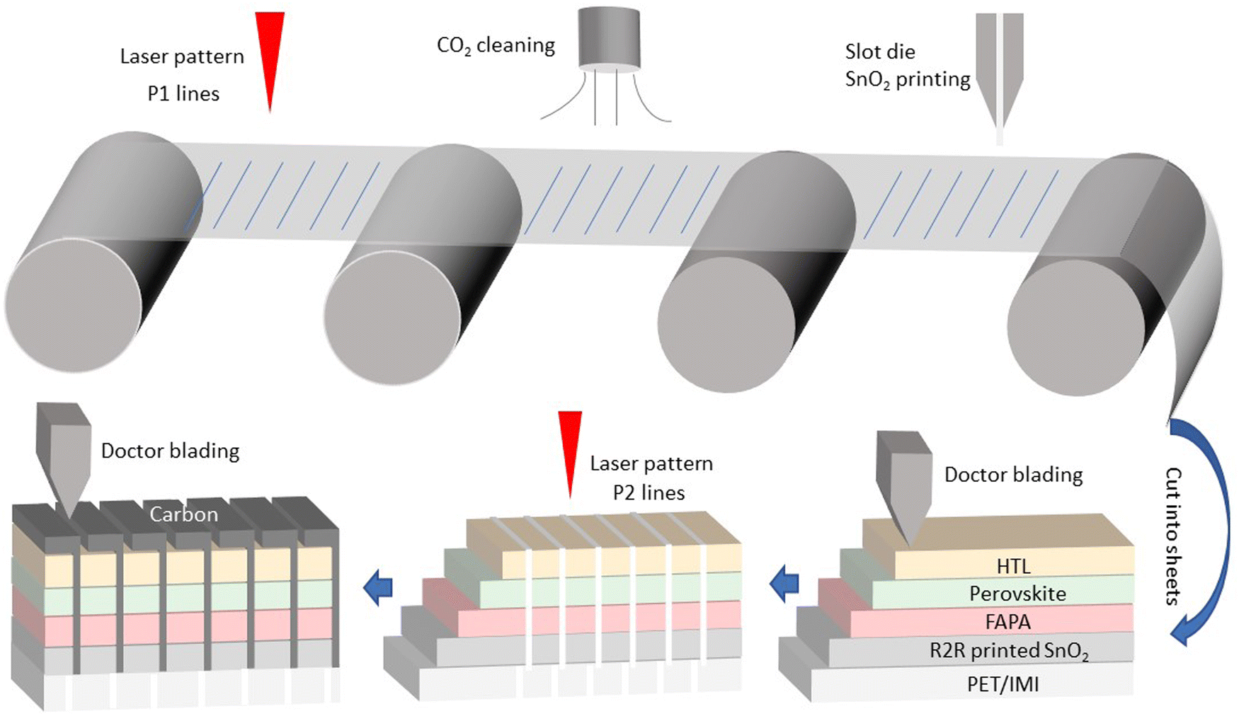 | ||
| Fig. 1 The workflow of manufacturing flexible perovskite solar modules, comprising laser patterning of the IMI bottom electrode, deburring by CO2 snow jet cleaning, R2R slot-die coating of the ETL, deposition of FAPA interface dipole layer, perovskite active layer and HTL by doctor blading, laser patterning of the active layer stack (P2), and deposition of the carbon electrode by stencil printing (P3). Manufacturing of perovskite solar cells follows the same workflow, but without the laser patterning steps P1–P3 (for details see the experimental part in the ESI†). | ||
Impact of SnO2 surface modification on solar cell performance
We first consider reducing ETL/perovskite interfacial recombination in small-area f-PSCs (Fig. 2a), through modification of the SnO2 surface with a thin layer of fullerene alkylphosphonic acids (FAPA). As shown in Fig. 2b, two different fullerene alkyl phosphonic acids, mono(alkylphosphonic acid)fullerene (referred to as “monoFAPA”) and bis(alkylphosphonic acid)fullerene (referred to as “bisFAPA”), are investigated. | ||
| Fig. 2 (a) Photograph of f-PSCs. (b) Chemical structures of monoFAPA and bisFAPA. (c) Representative J–V curves measured with forward scanning (FS) and reverse scanning (RS) for reference and FAPA-modified devices. (d) and (e) Illumination stability under 1 sun and 65 °C in nitrogen atmosphere with bisFAPA modified device. (f) Normalized PCE of f-PSCs as a function of the number of mechanical bending cycles. The insert figure shows a photograph of the bending test. | ||
Representative current density–voltage (J–V) curves of the optimized FAPA layers are plotted in Fig. 2c, as compared to a reference device comprising unmodified SnO2. Modification of SnO2 by monoFAPA improves device performance, mainly contributed by an increase in average fill factor (FF) from 53% to 64% and an improvement of the average VOC by 50 mV, whilst modification by bisFAPA leads to an even greater improvement of FF to 69% and of VOC by 100 mV with respect to the reference (for detailed parameters see Fig. S1 and S2, ESI†). Obviously, bisFAPA outperforms monoFAPA in terms of modifying the SnO2 surface. The champion cell thus achieved by using bisFAPA shows a short-circuit current density (JSC) of 21.7 mA cm−2, VOC of 1.09 V, FF of 72% and PCE of 17.0%. The JSC measured from J–V scan is in acceptable agreement with the integrated JSC from external quantum efficiency (EQE) measurements, which show values of around 20.0 mA cm−2 (Fig. S3, ESI†).
Notably, as shown in Fig. 2c, whilst the reference device exhibits significant J–V hysteresis, it is reduced for the monoFAPA modified devices and is almost completely absent for the bisFAPA modified devices. The observed phenomenon is likely a result of the diminished density of trap defects within the perovskite and suppressed ions movement due to the insulating nature properties of FAPA layer.24 The champion cell with bisFAPA shows steady-state power output (SPO) of 16.7% through 100 seconds photocurrent measurement at the maximum power point, as demonstrated in Fig. S4 (ESI†), higher than that of the monoFAPA modified device (13.1%) and the reference device (10.0%). To our knowledge, this is the highest value ever reported for fully printed f-PSCs.
The devices with carbon electrodes have been compared to analogous devices with vapor-deposited metal (Ag) electrodes with respect to efficiency and stability. The difference in performance between the two types of electrodes turns out to be negligible (Fig. S5, ESI†). The stability of the devices with carbon electrodes is significantly enhanced when compared to cells with metal electrodes, as demonstrated in our prior work.12–14
The operational lifetime tests of unencapsulated solar cells under 1 sun illumination, Fig. 2d and e, show impressive long-term stability upon modification by bisFAPA, with around 95% of the initial efficiency remaining after 1200 h aging. In comparison, monoFAPA-modified devices exhibit 85% retention, while the SnO2 devices show only 55% of their initial PCE (Fig. S6, ESI†). Finally, the stability against bending was tested. Evolution of PCE during bending test of the f-PSCs, Fig. 2f, highlights improved mechanical stability of bisFAPA-modified interfaces, after 3000 bending cycles with a bending radius of 5 mm, the devices maintain 95% of their initial PCE. In comparison, monoFAPA-modified devices retain 88% of their initial PCE, while the reference SnO2 devices show a lower retention of only 80%. The original average PCEs are depicted in Fig. S7 (ESI†). This underscores the significantly superior mechanical stability of bisFAPA-modified interfaces when compared to both monoFAPA and the SnO2 based devices.
Crystallization of perovskite on FAPA modified interfaces
In order to elucidate the impact of interfacial modification by FAPA on the improved performance and stability, an investigation into the crystallization of perovskite on diverse interfaces is undertaken. Primarily, the bisFAPA exhibits significantly enhanced solubility in 1-butanol (Fig. S8, ESI†), due to improved hydrophilicity of the molecule by doubling the substitution of the fullerene moiety with phosphonic acids. The devices obtained upon optimizing the scalable deposition of FAPA by blade coating show comparable performance compared to those prepared by spin-coating the ETL with FAPA (Fig. S9, ESI†). Secondly, as illustrated in Fig. S10 (ESI†), the increased water contact angle, transitioning from 52° to 69° on SnO2 modified with monoFAPA and bisFAPA, respectively, signifies the reducing surface energy upon modification of the SnO2 surface with double phosphonic acid substituted fullerene compared to monoFAPA. The enhanced hydrophobicity results from a denser surface coverage of SnO2 in the case of bisFAPA. The increased hydrophobicity of the surface leads to improved crystal grains of the perovskite grown on top of the SnO2 layer, probably due to suppressed nuclei formation in the initial phase of film formation, in agreement with previous reports.25–27 The ultimate perovskite morphology on various interfaces is revealed in the cross-sectional scanning electron microscope (SEM) image in Fig. 3a–c. The contact on bare SnO2 exhibits small crystals with a random distribution, resulting in an undesired interfacial contact. In contrast, a noticeable enlargement of crystal size is observed on the FAPA-modified interface, particularly on the bisFAPA. Moreover, the differences discernible in the SEM cross sections are accentuated in the X-ray diffraction (XRD) pattern in Fig. 3d–f. The increased intensity of the (110) crystal plane, particularly evident upon bisFAPA modification, signifies an enhanced order of crystallinity and an increase in crystal size. Furthermore, the full-width at half maximum (FWHM) of the (110) and (220) peaks in the unmodified reference decreases by 63% and 41%, respectively with bisFAPA modification. This reduction further indicates an enhanced crystalline quality and improved buried contact. These outcomes consistently affirm the enhanced crystallinity and improved morphology of perovskite films on enhanced interfaces. The resulting elevated quality of perovskite elucidates the observed commendable stability under both, illumination and mechanical stress. As depicted in Fig. 3g–i, the perovskite film exhibits barely no cracks on FAPA modified interfaces, even after enduring 3000 bending cycles. The resulting response can explain why the device was able to maintain 95% of its initial PCE in the bending test.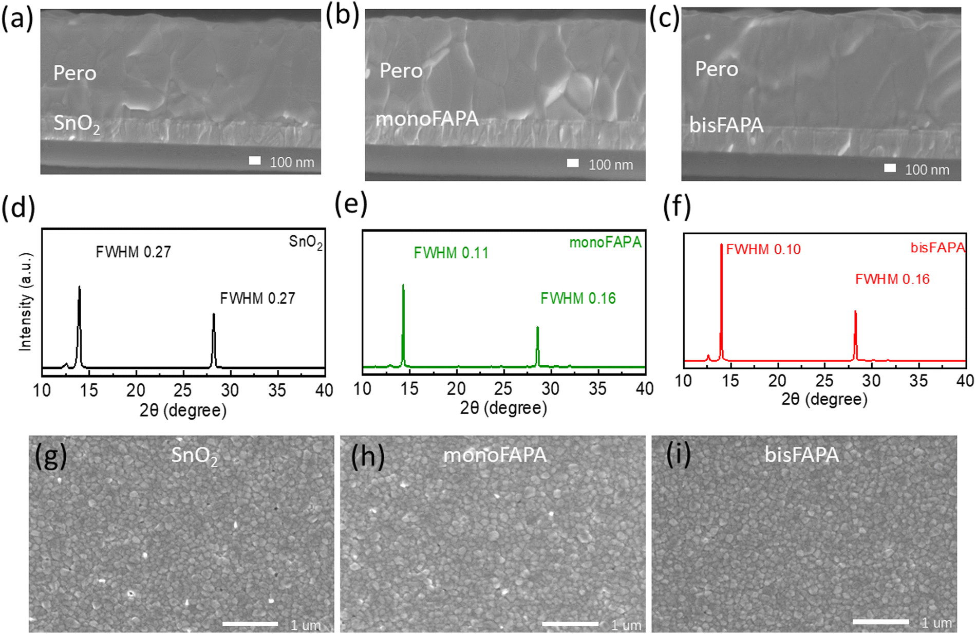 | ||
| Fig. 3 (a)–(c) Cross-sectional SEM of perovskite on SnO2, monoFAPA and bisFAPA modified SnO2 interfaces. (d)–(f) the XRD pattern of perovskite on bare SnO2 and two FAPA modified interfaces. (g)–(i) Top-view of perovskite on different interfaces after 3000 bending circles. | ||
Effects of FAPA on SnO2 electronic structure
To understand the role of FAPA in device improvement, we turn to investigate how it chemically and electronically affects the SnO2 interface. X-ray photoelectron spectroscopy (XPS) measurements prove the presence of FAPA on the SnO2 surface through the conspicuous phosphorus signals in the XPS spectrum (Fig. S11, ESI†). Fig. 4a displays the narrow XPS scans of the Sn 3d core level measured on the SnO2, SnO2/monoFAPA, and SnO2/bisFAPA surfaces. The intensity of the Sn 3d peak decreases significantly upon modification of the SnO2 layer by monoFAPA and is further reduced in the case of bisFAPA, suggesting that bisFAPA provides a much denser fullerene layer than monoFAPA, which is likely due to the enhanced chemical interaction with the SnO2 surface provided by two phosphonic groups per molecule. A rough estimate of the effective film thicknesses of FAPA layers on top of SnO2 is obtained from the drop of the Sn signal in the XPS spectrum, yielding values of approximately 1–3 nm, by using the Beer–Lambert law: x = −(1/α) × ln(I/I0), where I is the measured intensity of the Sn signal, I0 is the initial intensity of the Sn signal (reference), α is the attenuation factor and x is the effective film thickness of the FAPA layer.28–30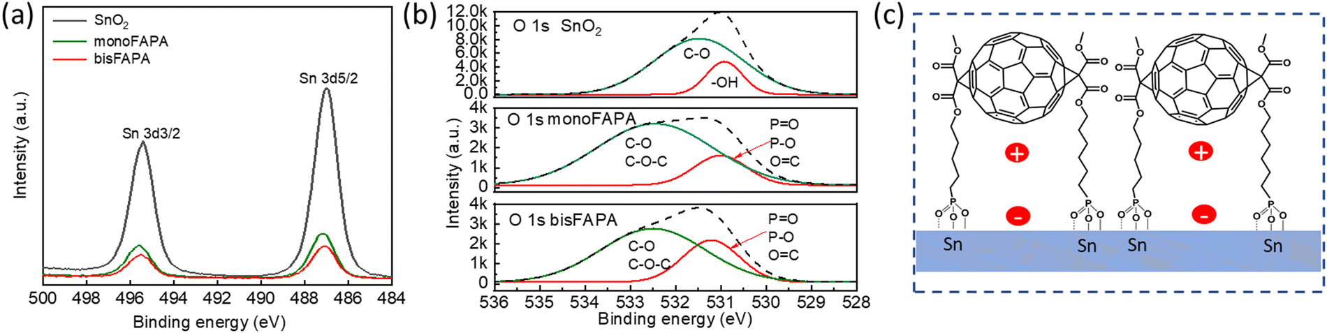 | ||
| Fig. 4 (a) XPS spectra of Sn 3d. (b) O 1s XPS on thin films of SnO2, SnO2 modified with monoFAPA and bisFAPA, respectively. The dashed lines represent the raw data, while the solid lines represent the peak signal that has been fitted. The C–O peak on SnO2 surface likely stems from the ligands contained in the SnO2 nanoparticle ink. (c) Schematic illustration of bisFAPA bonding to the SnO2 surface. | ||
The XPS O 1s spectra in Fig. 4b demonstrate a substantial chemical reaction between phosphonic acids and the hydroxyl groups (–OH) at the SnO2 surface. Capping the SnO2 surface with FAPA thin films results in a marked reduction in the intensity of –OH groups due to heterocondensation with the phosphonic acid group by formation of Sn–O–P bonds,31–33 while part of the observed effect may also be attributed to the increased escape depth of electrons that originate from the –OH groups, by the presence of the FAPA layer.34 In comparison to monoFAPA, bisFAPA exhibits a more pronounced O![[double bond, length as m-dash]](https://www.rsc.org/images/entities/char_e001.gif) P peak, at an approximately unchanged O–C signal, suggesting that the surface density of fullerene moieties is similar for both FAPA derivatives.35 Consequently, the surface density of phosphonic acid groups on bisFAPA-modified SnO2 is about twice that of monoFAPA, which leads to an overall higher surface coverage in the case of the latter. Fig. 4c illustrates the OP binding of bisFAPA to the SnO2 surface, which leads to the formation of a dipole layer, with the dipole moment pointing towards the SnO2 surface.36 Due to the higher number of phosphonic acid groups per fullerene molecule, the dipole moment is expected to be higher for bisFAPA layers than for those formed from monoFAPA.
P peak, at an approximately unchanged O–C signal, suggesting that the surface density of fullerene moieties is similar for both FAPA derivatives.35 Consequently, the surface density of phosphonic acid groups on bisFAPA-modified SnO2 is about twice that of monoFAPA, which leads to an overall higher surface coverage in the case of the latter. Fig. 4c illustrates the OP binding of bisFAPA to the SnO2 surface, which leads to the formation of a dipole layer, with the dipole moment pointing towards the SnO2 surface.36 Due to the higher number of phosphonic acid groups per fullerene molecule, the dipole moment is expected to be higher for bisFAPA layers than for those formed from monoFAPA.
The modification of SnO2 by FAPA is further supported by impedance measurements of the f-PSCs. The Nyquist plots shown in Fig. S12 (ESI†) are obtained by oscillating the frequency from 0.1 Hz to 1 MHz in the dark at open circuit conditions. The data are interpreted in terms of an equivalent circuit which assigns the semicircle to the SnO2/perovskite interface, represented by a recombination resistance (Rrec) and a capacitor.37,38 The recombination resistance increases from Rrec = 36.8 kΩ for the unmodified SnO2 to Rrec = 48.9 kΩ for the monoFAPA-modified ETL and further to Rrec = 74.5 kΩ for bisFAPA. The observed rise in recombination resistance is attributed to a denser FAPA layer, providing improved surface coverage and acting as an electric barrier against the recombination of electrons and holes.39 Furthermore, it is interesting to note that this increase of contact resistance at the SnO2/perovskite interface shows the same trend as the suppression of hysteresis. This effect is at least partially attributable to reduced ionic defect density in the bulk of perovskite due to improved crystal growth on top of the FAPA layers, as demonstrated in the previous section.
To provide a measure for the effect of SnO2 modification by FAPA on perovskite crystal quality, we have estimated the charge carrier trap density in modified and unmodified devices, by employing the space-charge-limited current (SCLC) technique using single charge-transporting structures. For this purpose, ETL-only devices composed of a PET/IMI/SnO2 layer, with and without FAPA, followed by a perovskite layer, PCBM layer, and a carbon electrode were fabricated. Fig. S13 (ESI†) displays a logarithmic presentation of the dark I–V curves, contrasting devices with and without fullerene derivatives at the interface. In the low bias voltage regime, a linear response, indicative of ohmic behaviour is observed. As bias voltage increases, a significant rise in current injection occurs in the intermediate region. It is obvious that the introduction of monoFAPA and bisFAPA layers onto the SnO2 surface leads to a reduction in trap-filling voltage (VTFL). Consequently, the trap density (Nt) within the devices is derived from the following relationship:40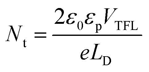 , where ε0 is the vacuum dielectric constant, e is the electron charge, εp is the perovskite dielectric constant, and LD is the perovskite layer thickness. The trap density in the bulk perovskites decreases from 9.4 × 1015 cm−3 for unmodified SnO2 to 8.9 × 1015 cm−3 and 7.4 × 1015 cm−3 for monoFAPA and bisFAPA, respectively, confirming an improved quality of perovskite films grown on FAPA-modified SnO2. Moreover, according to ref. 40, the reduced trap density could also originate from the suppressed ion movement by the FAPA layer due to its insulating nature resulting in negligible hysteresis in the FAPA modified devices.
To understand how the FAPA modification and the resulting energy level alignment at the SnO2/perovskite interface affect device performance, we turn to ultraviolet photoelectron spectroscopy (UPS) measurements. The presence of the dipole layer formed by FAPA generates a localized electric field at the SnO2/perovskite interface which upshifts the Fermi level (EF) of SnO2, as shown in Fig. 5a. The EF values are determined from the positions of the secondary electron cut-off energies (Ecut-off) by the equation EF = hv − Bias − Ecut-off. The EF values of SnO2 thus calculated decrease from −4.80 eV to −4.52 eV upon modification of SnO2 with monoFAPA, and further drop to −4.41 eV for bisFAPA, in accordance with the expected stronger interface dipole created by the latter. These values agree with the work functions of the corresponding samples determined by Kelvin probe measurements (Fig. S14, ESI†).
 | ||
| Fig. 5 (a) UPS spectra showing the secondary cut-off energies and the resulting Fermi levels of the SnO2 surfaces with and without FAPA modification. (b) PLQY and QFLS of the perovskite on bare SnO2, SnO2/monoFAPA and SnO2/bisFAPA. (c) Differential transient lifetimes of perovskite on bare SnO2, SnO2/monoFAPA and SnO2/bisFAPA at a laser fluence of 12 nJ cm−2. (d) Schematic drawing of the energy band diagram at the interface between perovskite and the unmodified SnO2 interface. (e) Schematic drawing of the energy band diagram of the interface between perovskite and FAPA-modified SnO2. (f) Simulated JV curves match well with the experimental results. | ||
The impact of energy level alignment on interfacial charge recombination is quantified by measurements of photoluminescence quantum yield (PLQY) and time-resolved PL decay traces. Fig. 5b shows the measured PLQY of perovskite coated on bare SnO2 and SnO2 modified with interface dipole layer. Notably, the introduction of FAPA dipole layers on top of SnO2 leads to an enhancement in PLQY, by a factor of 2.1 for monoFAPA and by a factor of 7.3 for bisFAPA, in accordance with the PL decay times extracted from Fig. S15 (ESI†). The enhanced PL lifetimes are clearly demonstrated by the differential lifetime plot shown in Fig. 5c. A higher differential lifetime corresponds to lower surface recombination at low injection due to less charge carrier accumulation at interfaces (details of the calculations are provided in ESI†).41 The corresponding minority carrier lifetimes obtained by fitting bi-exponential decay functions to the decay curves are shown in Table S1 (ESI†).
This increase in PLQY and PL lifetime is explained by the strongly reduced interfacial non-radiative recombination upon the introduction of the FAPA interface dipole layer as illustrated in Fig. 5d and e. A significant energetic offset between the ETL and perovskite promotes the recombination of electrons and holes through surface traps (Fig. 5d).42 Introducing an interface dipole layer by modification of SnO2 with FAPA elevates the Fermi level of the ETL, leading to a smaller offset of the conduction band minima at the SnO2/perovskite interface (Fig. 5e) and thus to reduced band bending at this interface under illumination, which in turn serves to efficiently release photogenerated charge carriers from the interface.42 The consequent diminution of interface charge carrier density effectively mitigates interface recombination. As in our system interface recombination is the dominating process of charge carrier loss, the effect of reinjection of extracted minority carriers is negligible, which overall leads to an increase of minority carrier lifetime. Consequently, the suppression of interface recombination, enabled by the reduced energetic offset, translates into an overall improvement in photovoltaic performance.
The effect of reduced interface recombination on quasi-Fermi level splitting (QFLS) is calculated according to QFLS = Vradoc (Eg) + kT![[thin space (1/6-em)]](https://www.rsc.org/images/entities/i_char_2009.gif) ln(PLQY), where the Vradoc is radiative Shockley–Queisser limit related to the optical bandgap of perovskite.43 The introduction of monoFAPA and bisFAPA thus results in a significant improvement of the external QFLS of the perovskite on SnO2, with values increasing from 1.01 eV for bare SnO2 to 1.08 eV and 1.12 eV, respectively. This result is in good agreement with the VOC values of our devices represented above.
ln(PLQY), where the Vradoc is radiative Shockley–Queisser limit related to the optical bandgap of perovskite.43 The introduction of monoFAPA and bisFAPA thus results in a significant improvement of the external QFLS of the perovskite on SnO2, with values increasing from 1.01 eV for bare SnO2 to 1.08 eV and 1.12 eV, respectively. This result is in good agreement with the VOC values of our devices represented above.
To further evaluate how energy level alignment affects device performance, we turn to drift-diffusion simulations of f-PSCs using the open-source package SIMsalabim to perform the simulations and BOAR to perform the JV fitting using Bayesian optimization.44–48 The primary parameter under investigation is the layer stack of SnO2 with FAPA modification. Other parameters, such as the energetics of SnO2 and the interfacial trap density, are incorporated into the simulation based on experimental results and documented data (Table S2, ESI†). The simulated JV curves under 1 sun illumination, Fig. 5f, show a good match with the experimental JV curves. The device with the interface dipole modified SnO2 outperforms the device with only bare SnO2, due to increased VOC and FF. The simulation results confirm the effectiveness of the introduced interface dipole on SnO2 in reducing interfacial recombination between ETL and perovskite.
We can more quantitively describe the contributions from energetic offset and interfacial traps to the overall interfacial recombination rate (wint), through the equation 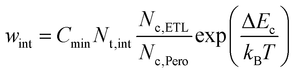 ,49 where Cmin is minority carrier capture coefficient, and Nt,int is the interfacial trap density determined from the trPL lifetime, as detailed in the ESI.†Nc,ETL and Nc,Pero are the effective densities of states of ETL and perovskite, respectively. ΔEc is the energetic offset between conduction band (CB) of perovskite and CB of ETL and kBT is thermal energy. From bare SnO2 to monoFAPA and bisFAPA modification, the decreased energetic offset ΔEc reduces wint from 7.53 × 10⁴ m−1 s−1 to 7.99 × 10³ m−1 s−1 by monoFAPA and further to 3.04 × 101 m−1 s−1 by bisFAPA (Table S2, ESI†). The trend observed in the simulation, where a significant reduction in interfacial recombination rates is achieved by lowering the energetic barrier between ETL and the perovskite, aligns with the trend observed in our experiments through the decrease in the WF of the ETL as measured by UPS. This supports our hypothesis that the introduction of a thin dipole layer in the ETL alters the electronic energy band structure at the ETL interface, thus substantially reducing non-radiative recombination at the buried interface. Consequently, this enhancement in optoelectronic performance is evident in the improved device characteristics.
Upscaling solar module fabrication
Having demonstrated the beneficial impact of FAPA interlayers on solar cell performance, in the last section, we turn to consider upscaling the production of bisFAPA-modified f-PSMs.Fig. 6a shows a photograph of the f-PSM consisting of seven solar cells connected in series, with an active area of 2.41 cm2 for each individual cell and a total aperture area of 20.25 cm2 on flexible substrate. As illustrated in Fig. 6b, the cell interconnection within the module requires three parallel scribes designated as P1, P2, and P3. To electrically separate the IMI bottom electrode into the desired number of individual cells, P1 lines are scribed on flexible PET/IMI sheets using a femtosecond laser with a fluence of 400 μJ cm−2. The spikes that are typically formed by laser ablation of IMI films are removed afterwards by R2R CO2 snow jetting.50 After coating the functional layers on the P1 patterned IMI substrates, P2 lines are laser-ablated, which serves as a prerequisite for the electrical interconnection of adjacent cells upon coating the top carbon electrode.
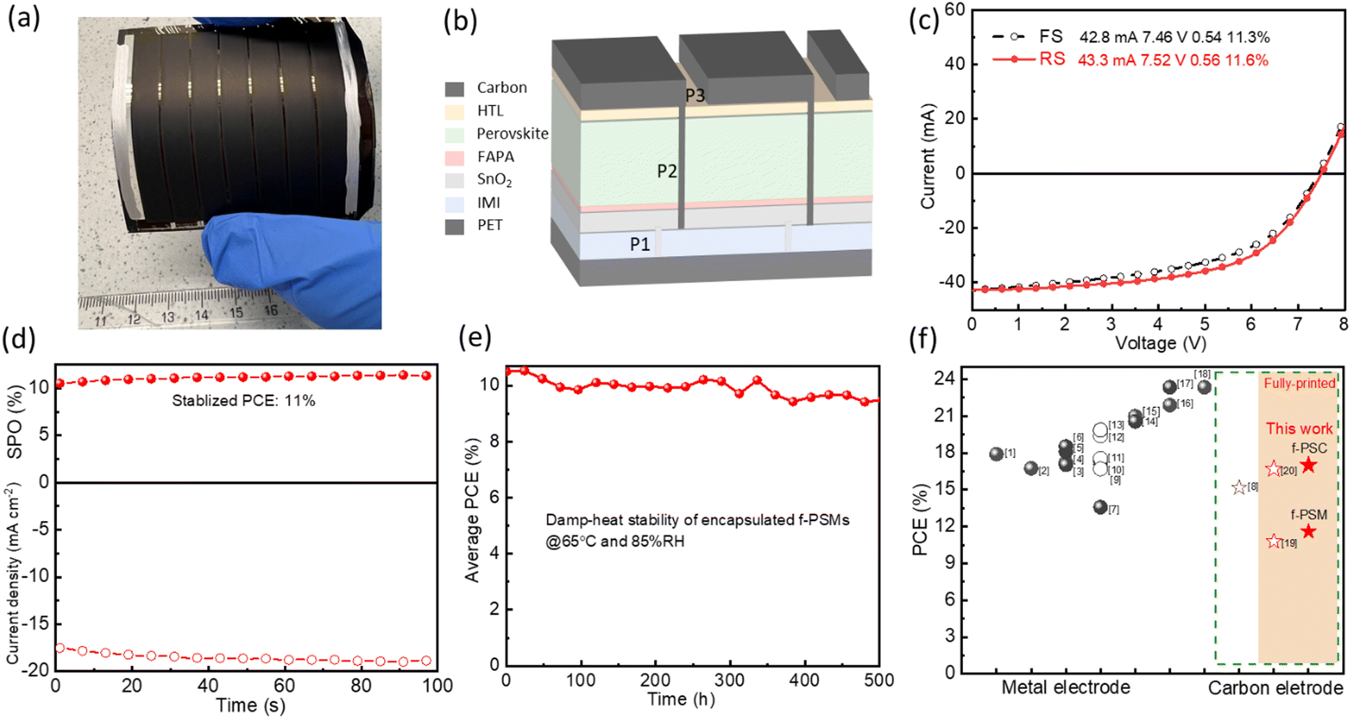 | ||
| Fig. 6 (a) Photograph of f-PSM on an total area of 25 cm2 plastic substrate. (b) Cross-sectional schematic drawing showing how individual cells are connected in series to form the thin-film solar modules. (c) I–V curves of the champion flexible module measured with FS and RS. (d) SPO of the f-PSM with bisFAPA modification. (e) Damp-heat stability test for encapsulated f-PSMs in the best condition with bisFAPA modification. (f) Overview of PCE of f-PSCs deposited by spin coating (solid black circle) and scalable techniques (open black circle) with evaporated metal electrodes and fully printed f-PSCs with carbon electrode (light red area). The numbers behind the dots refer to the corresponding references which can be found in the ESI.† | ||
The resulting champion module manufactured with the bisFAPA modified SnO2 layer shows a PCE of 11.6% (VOC = 7.52 V, ISC = 43.3 mA and FF = 56%), with minimized hysteresis, Fig. 6c. The SPO, by holding the module at the voltage of maximum power point and measuring the photocurrent, is 11.0% as shown in Fig. 6d. Finally, we conducted a damp-heat test on the encapsulated f-PSMs. The modules are encapsulated inside a barrier foil, carried out under inert conditions using rim type encapsulation as depicted in Fig. S16 (ESI†). Subsequently, the encapsulated f-PSMs are subjected to accelerated lifetime testing under damp heat conditions using ISOS-D3 (65 °C and 85% RH) as the test standard (Fig. S17, ESI†).51 As depicted in Fig. 6e, these modules maintain approximately 90% of their initial PCE after a 500 h test period.
To underline the significance of this work, we summarize in Fig. 6f the recent advancements in the efficiency of f-PSCs. Details of device parameters are shown in Table S3 (ESI†). The majority of the state-of-art f-PSCs reported over the past eight years were fabricated using the spin-coating technique and evaporated metal as top electrode. Among the fully printed f-PSCs with carbon electrode reported so far, this work presents the highest PCE. Most importantly, this work represents the highest PCE reported on a fully printed f-PSM with metal-free electrode. A fully printed perovskite module on flexible substrate with a PCE of 11.6% represents a significant advancement in the field of printed perovskite PV.
Conclusions
This study presents the scalable fabrication of efficient, fully printed f-PSMs comprising printed carbon top electrodes, through careful optimization of interfacial modifier, layer coating conditions and laser scribing parameters. Special attention has been paid to the perovskite/ETL interface, at which non-radiative recombination loss has been substantially reduced by the construction of a continuous and dense FAPA thin layer on top of the SnO2 layer, leading to remarkable improvement in VOC and FF. We find that an interfacial dipole layer is formed, through strong chemical bonding between phosphonic acid and the hydroxyl groups of SnO2, which reduces the WF of SnO2 and thus the energetic offset with respect to the perovskite layer. Through the refinement of all interfaces via scalable coating methods, PCE values of 17.0% and 11.6% for f-PSCs and f-PSMs have been achieved, respectively, with long-term mechanical durability and consistent operational stability. These findings, particularly the production of large-scale flexible modules, achieve substantial progress toward the eventual commercialization of printable perovskite PV.Author contributions
L. D. performed the experiments and wrote the manuscript. S. Q. was involved in the discussion of the manuscript. J. G. C. made the module layout. M. W. and C. A. technically support roll-to-roll line. O. K. organized and measured XPS measurements. H. P. arranged the UPS measurements. S. F. encapsulated the flexible modules. D. J. and C. L. measured and analysed the PL data. K. Z. measured infrared absorption. V. L. C. did the simulation part. F. U. K. with C. D. and F. Y. modified the manuscript. C. J. B. and T. D. reviewed the manuscript. H.-J. E. supervised the work and the writing of the manuscript. All the co-authors discussed the results and commented on the manuscript.Data availability
The data that support the findings of this study are available in the ESI† files.Conflicts of interest
The authors declare no conflict of interest.Acknowledgements
The Solar Factory of the Future (SFF) as part of the Energy Campus Nürnberg (EnCN) is acknowledged, which is supported by the Bavarian State Government (FKZ 20.2-3410.5-4-5). Part of this work has been supported by the Helmholtz Association in the framework of the innovation platform “Solar TAP”. T. D. acknowledges the financial support from Deutsche Forschungsgemeinschaft (DFG) via the Perovskite SPP2196 program (project no. 506698391). L. D. gratefully acknowledges funding of the Erlangen Graduate School in Advanced Optical Technologies (SAOT) by the Bavarian State Ministry for Science and Art. L. D. acknowledges Sven Boelke and Ivana Mrsic for XPS measurements. S. Q. and C. L. are grateful for the support from the China Scholarship Council (CSC). J. G. C. gratefully acknowledges the Deutscher Akademischer Austauschdienst (DAAD) for the granting of a doctoral scholarship. F. U. K. thanks the Jardine Foundation and Cambridge Trust for a doctoral scholarship. C. D. acknowledges European Union’s Horizon 2020 research and innovation program (823717–ESTEEM3). F. Y. acknowledges the financial support from the National Natural Science Foundation of China (Grant No. 52102287), Natural Science Foundation of Jiangsu Province (Grant No. BK20210731) and the Natural Science Foundation of the Jiangsu Higher Education Institutions of China (21KJD150003).References
- Z. Li, C. Jia, Z. Wan, J. Xue, J. Cao, M. Zhang, C. Li, J. Shen, C. Zhang and Z. Li, Nat. Commun., 2023, 14, 6451 CrossRef CAS PubMed.
- L. Xie, S. Du, J. Li, C. Liu, Z. Pu, X. Tong, J. Liu, Y. Wang, Y. Meng and M. Yang, Energy Environ. Sci., 2023, 16, 5423–5433 RSC.
- Y. Wu, G. Xu, J. Xi, Y. Shen, X. Wu, X. Tang, J. Ding, H. Yang, Q. Cheng and Z. Chen, Joule, 2023, 7, 398–415 CrossRef CAS.
- B. Dou, J. B. Whitaker, K. Bruening, D. T. Moore, L. M. Wheeler, J. Ryter, N. J. Breslin, J. J. Berry, S. M. Garner and F. S. Barnes, ACS Energy Lett., 2018, 3, 2558–2565 CrossRef CAS.
- D. Beynon, E. Parvazian, K. Hooper, J. McGettrick, R. Patidar, T. Dunlop, Z. Wei, P. Davies, R. Garcia-Rodriguez and M. Carnie, Adv. Mater., 2023, 35, 2208561 CrossRef CAS PubMed.
- T. Bu, J. Li, F. Zheng, W. Chen, X. Wen, Z. Ku, Y. Peng, J. Zhong, Y.-B. Cheng and F. Huang, Nat. Commun., 2018, 9, 4609 CrossRef PubMed.
- Y. Y. Kim, T.-Y. Yang, R. Suhonen, A. Kemppainen, K. Hwang, N. J. Jeon and J. Seo, Nat. Commun., 2020, 11, 5146 CrossRef CAS PubMed.
- H. C. Weerasinghe, N. Macadam and J.-E. Kim, Nat. Commun., 2024, 15, 1656 CrossRef CAS PubMed.
- F. Jafarzadeh, L. A. Castriotta, F. De Rossi, J. Ali, F. Di Giacomo, A. Di Carlo, F. Matteocci and F. Brunetti, Sustainable Energy Fuels, 2023, 7, 2219–2228 RSC.
- L. J. Sutherland, D. Vak, M. Gao, T. A. N. Peiris, J. Jasieniak, G. P. Simon and H. Weerasinghe, Adv. Energy Mater., 2022, 12, 2202142 CrossRef CAS.
- E. H. Jung, N. J. Jeon, E. Y. Park, C. S. Moon, T. J. Shin, T. Y. Yang, J. H. Noh and J. Seo, Nature, 2019, 567, 511–515 CrossRef CAS PubMed.
- F. Yang and L. Dong, Adv. Energy Mater., 2021, 11, 2101219 CrossRef CAS.
- F. Yang, L. Dong and H. J. Egelhaaf, Adv. Energy Mater., 2020, 10, 2001869 CrossRef CAS.
- T. Du, S. Qiu, X. Zhou and H.-J. Egelhaaf, Joule, 2023, 7, 1920–1937 CrossRef CAS.
- F. Giordano, A. Abate, J. P. Correa Baena, M. Saliba, T. Matsui, S. H. Im, S. M. Zakeeruddin, M. K. Nazeeruddin, A. Hagfeldt and M. Graetzel, Nat. Commun., 2016, 7, 10379 CrossRef CAS PubMed.
- Z.-L. Tseng, C.-H. Chiang and C.-G. Wu, Sci. Rep., 2015, 5, 13211 CrossRef CAS PubMed.
- S. Y. Park and K. Zhu, Adv. Mater., 2022, 34, 2110438 CrossRef CAS PubMed.
- Z. Li, T. R. Klein, D. H. Kim, M. Yang, J. J. Berry, M. F. Van Hest and K. Zhu, Nat. Rev. Mater., 2018, 3, 1–20 CrossRef CAS.
- M. Valles-Pelarda, B. C. Hames, I. Garcia-Benito, O. Almora, A. Molina-Ontoria, R. S. Sanchez, G. Garcia-Belmonte, N. Martin and I. Mora-Sero, J. Phys. Chem. Lett., 2016, 7, 4622–4628 CrossRef CAS PubMed.
- D. Garcia Romero, L. Di Mario, F. Yan, C. M. Ibarra-Barreno, S. Mutalik, L. Protesescu, P. Rudolf and M. A. Loi, Adv. Energy Mater., 2023, 2307958 Search PubMed.
- G. Tumen-Ulzii, T. Matsushima, D. Klotz, M. R. Leyden, P. Wang, C. Qin, J.-W. Lee, S.-J. Lee, Y. Yang and C. Adachi, Commun. Mater., 2020, 1, 31 CrossRef.
- Y. Hou, S. Scheiner and C. J. Brabec, Adv. Mater. Interfaces, 2017, 4, 1700007 CrossRef.
- Y. Hou, X. Du, S. Scheiner, D. P. McMeekin, Z. Wang, N. Li, M. S. Killian, H. Chen, M. Richter and I. Levchuk, Science, 2017, 358, 1192–1197 CrossRef CAS PubMed.
- B. Chen, M. Yang and S. Priya, J. Phys. Chem. Lett., 2016, 7, 905–917 CrossRef CAS PubMed.
- D. Liu, Z. Shao and J. Gui, Chem. Commun., 2019, 55, 11059–11062 RSC.
- C. Bi, Q. Wang, Y. Shao, Y. Yuan, Z. Xiao and J. Huang, Nat. Commun., 2015, 6, 7747 CrossRef CAS PubMed.
- W. A. Dunlap-Shohl, Y. Zhou, N. P. Padture and D. B. Mitzi, Chem. Rev., 2019, 119, 3193–3295 CrossRef CAS PubMed.
- D. Y. Zemlyanov, M. Jespersen and D. N. Zakharov, Nanotechnology, 2018, 29, 115705 CrossRef PubMed.
- P. J. J. S. Cumpson, Interfaces Thin Films, 2000, 29, 403–406 CAS.
- F. A. Stevie and C. L. Donley, J. Vac. Sci. Technol., A, 2020, 38, 063204 CrossRef CAS.
- P. H. Mutin, G. Guerrero and A. Vioux, J. Mater. Chem. A, 2005, 15, 3761–3768 RSC.
- S. A. Paniagua, P. J. Hotchkiss and S. C. Jones, J. Phys. Chem. C, 2008, 112, 7809–7817 CrossRef CAS.
- S. Pawsey, K. Yach and L. Reven, Langmuir, 2002, 18, 5205–5212 CrossRef CAS.
- F. Ahimou, C. J. Boonaert, Y. Adriaensen, P. Jacques, P. Thonart, M. Paquot and P. G. Rouxhet, J. Colloid Interface Sci., 2007, 309, 49–55 CrossRef CAS PubMed.
- E. Yalcin, M. Can, C. Rodriguez-Seco, E. Aktas, R. Pudi, W. Cambarau, S. Demic, E. J. E. Palomares and E. Science, Energy Environ. Sci., 2019, 12, 230–237 RSC.
- R. Wick-Joliat, T. Musso, R. R. Prabhakar, J. Löckinger, S. Siol, W. Cui, L. Sévery, T. Moehl, J. Suh and J. J. E. Hutter, Energy Environ. Sci., 2019, 12, 1901–1909 RSC.
- F. Ebadi, N. Taghavinia, R. Mohammadpour, A. Hagfeldt and W. Tress, Nat. Commun., 2019, 10, 1574 CrossRef PubMed.
- A. Guerrero, J. Bisquert and G. Garcia-Belmonte, Chem. Rev., 2021, 121, 14430–14484 CrossRef CAS PubMed.
- E. Von Hauff and D. Klotz, J. Mater. Chem. C, 2022, 10, 742–761 RSC.
- V. M. Le Corre, E. A. Duijnstee, O. El Tambouli, J. M. Ball, H. J. Snaith, J. Lim and L. J. A. Koster, ACS Energy Lett., 2021, 6, 1087–1094 CrossRef CAS PubMed.
- L. Kruckemeier, Z. Liu and T. Kirchartz, Adv. Mater., 2023, 35, e2300872 CrossRef PubMed.
- L. Krückemeier, B. Krogmeier, Z. Liu and T. Kirchartz, Adv. Energy Mater., 2021, 11, 2003489 CrossRef.
- M. Stolterfoht, P. Caprioglio, C. M. Wolff, J. A. Márquez, J. Nordmann, S. Zhang, D. Rothhardt, U. Hörmann, Y. Amir, A. Redinger, L. Kegelmann, F. Zu, S. Albrecht, N. Koch, T. Kirchartz, M. Saliba, T. Unold and D. Neher, Energy Environ. Sci., 2019, 12, 2778–2788 RSC.
- https://github.com/kostergroup/SIMsalabim .
- https://github.com/i-MEET/boar .
- M. Wagner, A. Distler, V. M. L. Corre, S. Zapf, B. Baydar, H.-D. Schmidt, M. Heyder, K. Forberich, L. Lüer and C. Brabec, Energy Environ. Sci., 2023, 5454–5463 RSC.
- C. Liu, L. Lüer, V. M. L. Corre, K. Forberich, P. Weitz, T. Heumüller, X. Du, J. Wortmann, J. Zhang and J. Wagner, Adv. Mater., 2023, 2300259 Search PubMed.
- M. Koopmans, V. M. Le Corre and L. J. A. Koster, J. Open Source Softw., 2022, 7, 3727 CrossRef.
- M. Koopmans and L. J. A. Koster, Sol. RRL, 2022, 6, 2200560 CrossRef CAS.
- M. Wagner, A. Distler, H.-D. Schmidt, A. Classen, T. Stubhan, M. Koegl, J. Illg, C. Brabec and H.-J. Egelhaaf, Flex. Print. Electron., 2023, 8, 015007 CrossRef.
- M. V. Khenkin, E. A. Katz, A. Abate, G. Bardizza, J. J. Berry, C. Brabec, F. Brunetti, V. Bulović and Q. Burlingame, Nat. Energy, 2020, 5, 35–49 CrossRef.
Footnote |
| † Electronic supplementary information (ESI) available. See DOI: https://doi.org/10.1039/d4ee01647e |
| This journal is © The Royal Society of Chemistry 2024 |