
 Open Access Article
 This Open Access Article is licensed under a
 Creative Commons Attribution 3.0 Unported Licence
A new metallization method of modified tannic acid photoresist patterning†
Zicheng
Tang‡
,
Xubin
Guo‡
,
Haihua
Wang
 ,
Huan
Chen
and
Wenbing
Kang
*
,
Huan
Chen
and
Wenbing
Kang
*
National Engineering Research Center for Colloidal Materials, School of Chemistry and Chemical Engineering, Shandong University, Jinan, Shandong province 250100, China. E-mail: wbkang@sdu.edu.cn
First published on 15th August 2023
Abstract
Metal patterning from a modified tannic acid (TA-Boc-MA) photoresist and the processes are designed using protection of hydroxyl groups in tannic acid, formulation into a photoresist, an exposure and pattern treatment process, and metallization by electroless Ag deposition with silver ion solution.
Keywords: Tannic acid; Positive photoresist; Metallization method; Metal patterning; Ag pattern.
Surface patterning techniques for micro-nano structures are key to the rapid development of science and technology, which can be applied in many fields, such as integrated circuit manufacturing,1 light-emitting devices,2 solar cells,3 flexible electronics4,5 and so on.6,7 However, metallization of the pattern is an essential step in assembling various devices. In ex situ approaches of metal patterning, researchers usually use “metal ink” with the assistance of an inject printer or soft-lithography method to form patterns on different substrates.8–10 However, their industrial applications are restricted by poor performance owing to poor stability and dispersity of metal nanoparticles and lower resolution caused by the coffee ring effect and surface tension. In contrast, in situ approaches can provide better adhesion between nanoparticles and polymers, avoiding the aggregation of nanoparticles which can affect the performance of the device.11,12
With the increasing requirements for high resolution metal patterning, pioneers have developed a direct laser writing technique by combining in situ approaches with direct lithography to realize in situ dispersion of metal nanoparticles in polymers.13,14 However, the local hyper-thermal effects of the laser by direct photoradiation on the metal precursors in polymers can lead to uncontrollability of metal growth and aggregation of particles, resulting in the irreversible loss of photoelectric properties. Hence, in situ electroless deposition after lithography patterning may be a better choice for avoiding the growth and aggregation of metal particles in the polymers.15
Phenolic hydroxyl groups play a rather important role in in situ electroless deposition due to their strong interactions with various metal ions and their reduction ability.16,17 Tannic acid is rich in natural products, having an adjacent tri-hydroxyl structure (Scheme S1†), which greatly improves its ability to reduce metal ions.18 However, tannic acid often needs be modified by some hydrophobic groups to improve the resistance in an alkaline developer and solubility in organic solvent for application in the photoresist.19,20 Despite the fact that modified tannic acid has been applied in photoresist patterning, an in situ metallization method based on modified tannic acid photoresist patterning have not been seen yet and is still a challenge.
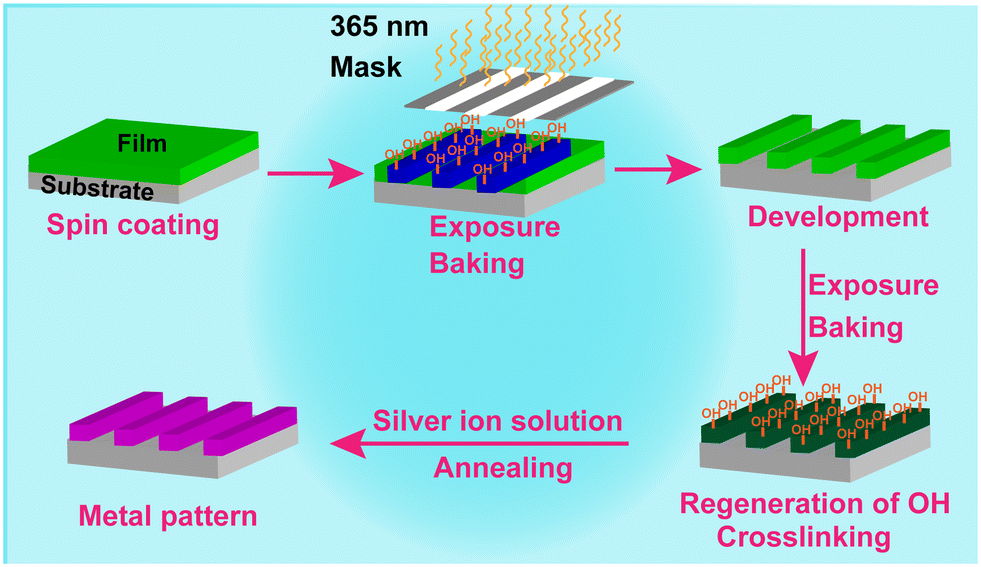
Herein, we would like to report a new process to conduct Ag patterning based on a newly modified tannic acid (TA-Boc-MA) positive photoresist. A TA-Boc-MA resin is designed by the reaction of tannic acid (TA) with di-tert butyl decarbonate (t-Boc) and methacryloyl chloride (MA), as shown in Scheme S2.† And then the TA-Boc-MA photoresist was blended with the TA-Boc-MA resin, photoacid generators and other additives (Table S1†). A schematic illustration of Au patterning is shown in Scheme 1, which includes two steps: (1) a lithographic pattern could be formed by the TA-Boc-MA photoresist through spin-coating, exposure, baking and development processes; (2) the Ag pattern is in situ assembled through the reduction of Ag+ to Ag nanoparticles utilizing the high reduction power of phenolic groups. However, Ag could not be deposited on the Si substrate owing to the lack of phenolic groups. The selective growth of Ag on the photoresist film with phenolic groups results in the formation of the Ag pattern.
 | ||
| Scheme 1 A schematic illustration of metal patterning based on the TA-Boc-MA photoresist. | ||
As seen from Scheme 1, there are two exposure and baking processes in the formation of the Ag pattern which are very unique in our process, during which several chemical reactions are undergoing (shown in Scheme S3†). A light source at 365 nm is the best option for Ag patterning, owing to the maximum UV absorption wavelength of the photoacid of 2-methyl-α-[2-[[(propylsulfonyl)oxy]imino]-3(2H)-thienylidene]benzene acetonitrile (PAG103) and radical generator of 2-(4-methoxystyryl)-4,6-bis(trichloromethyl)-1,3,5-triazine (3D) (Fig. S1†). After first exposure under a photomask with a light source at 365 nm, acids are generated by PAG103 (Scheme S3a†) in the exposed area which can catalyse the deprotection of t-Boc in the TA-Boc-MA resin via a subsequent baking procedure (Scheme S3b†).21 And then, the reappearance of the phenolic hydroxyl group (Fig. S2†) could accelerate the dissolution of the photoresist film in the exposed area in a developer of 2.38 wt% tetramethylammonium hydroxide (TMAH) solution, while the photoresist film in the unexposed area has low solubility in the developer, which can give the positive lithographic pattern. Next, the second exposure and baking could realize the regeneration of the phenol hydroxyl group at the unexposed area in the first exposure, preparing for Ag patterning. In the meantime, 3D can generate radicals (Scheme S3c†), creating cross-linking between TA-Boc-MA molecules or between TA-Boc-MA and pentaerythritol triacrylate (PETA) molecules,22 which could help in resisting the alkali plating solution. A schematic diagram of the cross-linking is shown in Scheme S4.† After exposure with a light source at 365 nm, the peak of the C![[double bond, length as m-dash]](https://www.rsc.org/images/entities/char_e001.gif) C stretches (∼1629 cm−1) weakened significantly (Fig. S3†), showing the success of the crosslinking process.23 In fact, the same chemical reaction happens during the two exposure and baking procedures and the crosslinking process also happens during the first exposure but does not affect the dissolution of the photoresist film in the developer at the exposed area. Therefore, a positive lithographic pattern could be achieved instead of a negative one. Although, the photoresist film in the exposed area could be dissolved in the TAMH developer but could not be dissolved in the alkali plating, which is because the pH (9.3) of the alkali plating solution is lower than the pH (13.5) of the TMAH developer. The same two exposure and baking procedures play different roles in the fabrication of the Ag pattern.
C stretches (∼1629 cm−1) weakened significantly (Fig. S3†), showing the success of the crosslinking process.23 In fact, the same chemical reaction happens during the two exposure and baking procedures and the crosslinking process also happens during the first exposure but does not affect the dissolution of the photoresist film in the developer at the exposed area. Therefore, a positive lithographic pattern could be achieved instead of a negative one. Although, the photoresist film in the exposed area could be dissolved in the TAMH developer but could not be dissolved in the alkali plating, which is because the pH (9.3) of the alkali plating solution is lower than the pH (13.5) of the TMAH developer. The same two exposure and baking procedures play different roles in the fabrication of the Ag pattern.
Fourier transform infrared spectroscopy (FTIR) of TA and the synthesized TA-Boc-MA samples were performed to confirm the successful synthesis of TA-Boc-MA (Fig. 1a). The peaks are assigned as O–H stretches (3429 cm−1), CO stretches (1714 cm−1), aromatic C–O symmetrical stretches (1620 cm−1) and aromatic C–O asymmetrical stretches (1314 cm−1 and 1620 cm−1) of TA molecules, respectively.24 The appearance of CC stretches (1637 cm−1), C–H stretches for methyl (2986 cm−1 and 2935 cm−1), C–H bending for tertiary butyl (1393 cm −1 and 1373 cm−1) and C–O–C stretches for ester bond of TA-Boc-MA molecules reveals the successful grafting of MA and t-Boc.21,23 At the same time, the O–H stretches (∼3429 cm−1) and aromatic C–O stretches of TA-Boc-MA molecules are sharply weakened and CO stretches shift from 1714 cm−1 to 1762 cm−1, due to the grafting of Boc and MA groups. The structure identification of synthesized TA-Boc-MA was further confirmed by 1H-NMR spectroscopy to certify successful grafting of the Boc group, as shown in Fig. 1b and S4.† The hydrogen-nuclear magnetic resonance (1H-NMR) peaks were (DMSO-d6, δ): 7–8.5 (phenyl ring), 5.6–6.2 (vinyl) and 0.9–1.5 (methyl in the tertiary butyl). According to the 1H-NMR results, the grafting molar ratios of t-Boc and MA on the phenolic group were calculated as 56% and 20%, respectively. The detailed calculated method and formula could be seen in the ESI.† The thermal degradation of Ta-Boc-Ma was evaluated with a thermogravimetric analyser (TGA) as shown in Fig. 1c. The 56% weight loss between 100 °C and 200 °C should be attributed to the decomposition of t-Boc.19
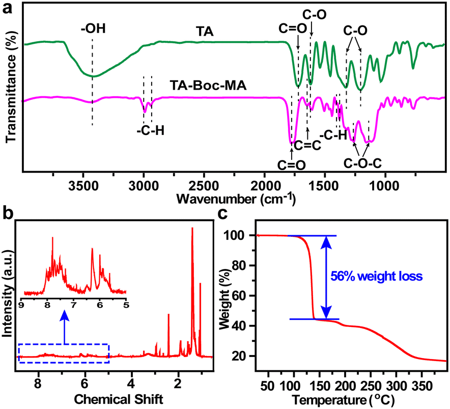 | ||
| Fig. 1 Structure characterization of TA and the synthesized TA-Boc-MA resin: (a) FTIR spectra of TA and TA-Boc-MA resin; (b) 1H-NMR spectra of TA-Boc-MA resin in DMSO-d6; (c) TGA analysis of the TA-Boc-MA resin. | ||
The TA-Boc-MA sample was employed as resin material to blend the photoresists. And then the resist films for fabricating the Ag pattern were obtained by spin-coating on the Si substrate and the thickness is about 800 nm. Fig. 2a shows the optical image of the lithographic pattern, displaying a clear pattern with a spacing of 10 μm and line width of 40 μm. The Ag pattern was constructed by immersing the film with the lithographic pattern into an electroless deposition solution. As seen in Fig. 2b, the Ag pattern is a complete replica of the lithographic pattern, indicating the triumph of the Ag patterning. To uncover the structure of the Ag pattern, cross-sectional scanning electron microscopy (SEM) and corresponding energy dispersive X-ray spectroscopy (EDX) mapping were conducted. The Ag pattern has a rough surface and its thickness is about 1.2 μm as shown in Fig. 2c. It is very clearly seen that the Ag pattern is composed of a lamellar structure and each silver layer is made up of silver nanoparticles bonded together. The emergence of silver nanoparticles should be attributed to the reduction of Ag+ adsorbed on the phenol hydroxyl group by the adjacent tri-hydroxyl structure to nucleate and then grow Ag.18 However, the surface of the Ag pattern changed from rough to smooth and the layer-by-layer structure disappeared after annealing at 200 °C for 10 minutes (Fig. 2d), possibly due to the melting of Ag nanoparticles and relocating evenly. Meanwhile, the thickness of the Ag pattern was shrunk to 670 nm, and reduced to about 44%. The cross-sectional SEM image (Fig. 2e) and its corresponding energy dispersive X-ray (EDX) mapping images (Fig. 2f–h) reveal that there are carbon and oxygen elements in addition to the silver element, which can be attributed to organic components in the photoresist film.
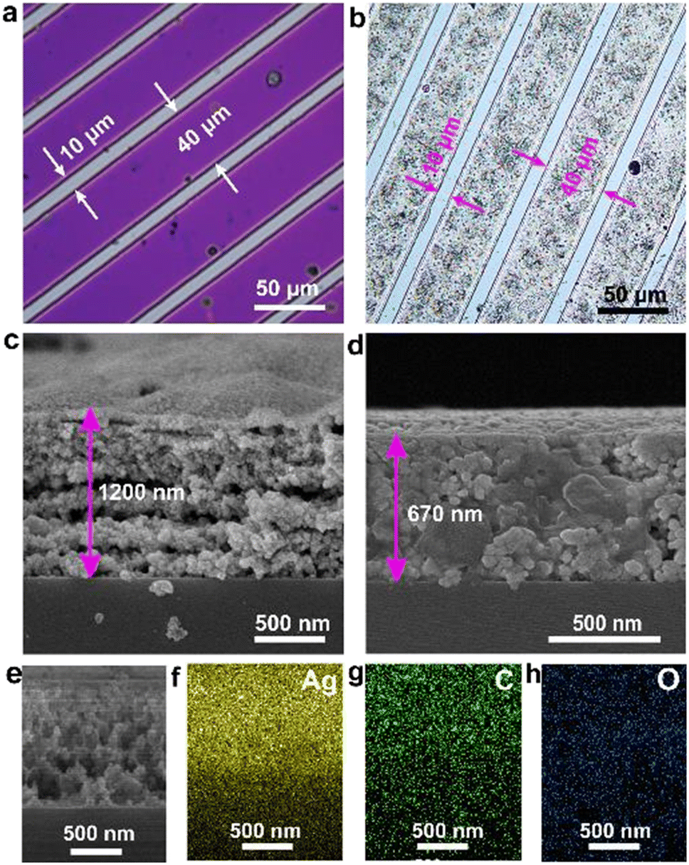 | ||
| Fig. 2 Optical images of the lithographic pattern (a) and the corresponding Ag pattern (b) based on the TA-Boc-MA photoresist exposed with a UV light source at 365 nm; cross-sectional SEM images of Ag pattern before (c) and after (d) annealing; cross-sectional SEM image of the Ag pattern (e) and the corresponding EDX mapping images (f–h) before annealing at 200 °C. Electroless deposition time for all the Ag patterns in Fig. 2 is 40 minutes. | ||
In addition, it was found that the thickness of the Ag pattern can be regulated by adjusting the soaking time in the electroless deposition solution. The cross-section SEM images at different electroless deposition times (Fig. 3) show that Ag nanoparticles on the substrate are grown layer by layer with a layer gap. With the increasing electroless deposition time, the layer gap becomes smaller while the thickness and layers of the pattern increases. When electroless plating for 10 minutes, only four layers of Ag are seen (Fig. 3a). Nevertheless, about eight layers of Ag are formed and the thickness reached ∼1.2 μm when soaking for 40 minutes (Fig. 3d). Meanwhile, the crystallinity becomes better with the extension of deposition time (Fig. S5†).
 | ||
| Fig. 3 SEM images of the Ag pattern at different electroless deposition times: (a) 10 min; (b) 20 min; (c) 30 min; (d) 40 min. | ||
To further verify the distribution of the silver element, Ag patterning on the silica substrate was analysed using X-ray photoelectron spectroscopy (XPS) spectra at different etching times (Fig. S6a†). With the increase of etching depth, the peak intensity decreases, suggesting that the silver content in the pattern is gradually decreasing. The result is also clearly displayed in Fig. S6b.† It is suggested that the structure of the Ag pattern changes from compact to loose with the increase of etching depth. Moreover, silicon substrate was also detected, further supporting the loose structure of the Ag pattern. The maximum percentage of silver atoms can be up to 80% on the surface of the Ag pattern (Fig. S6b†). In addition, the total amount of carbon and oxygen elements have remained at about 20%, indicating the residual amount of the photoresist after Ag patterning.
The measurement of square resistances of the Ag film without patterning is conducted to verify the conductivity of the film (Table S2†). With the increasing electroless deposition time, the square resistance of the Ag film decreases. When the Ag film was deposited for 40 minutes, the square resistance decreased to about 1 Ω sq−1, which could meet the needs of device assembly.
We are greatly encouraged by the success of the in situ Ag patterning onto the positive photoresist film. Due to the strong interaction of the TA anions and metal cations (Fe3+, Cu2+, Co3+, and so on),16 our new strategy could also be applied to metallization of other metals on lithographic patterns. In addition, a positive photoresist made of TA-Boc-MA can be coated not only on silicon wafers but also on other flexible substrates, such as polyethylene terephthalate film, polyimide film, flexible ITO and so on, which provides the possibility of applications for metallization of lithographic patterns in micro-nano circuits and other flexible devices.
In summary, a new unique process for metallization of lithographic patterns was discovered. Firstly, the TA-Boc-MA resin was designed by grafting both Boc and MA groups in tannic acid, which was employed to blend to the TA-Boc-MA photoresist. And then, the lithographic pattern was prepared by the first process of exposure with a mask, baking and development. After secondary exposure and baking, the phenolic hydroxyl group of the TA-Boc-MA photoresist on the pattern could be regenerated. Finally, the Ag pattern could be in situ constructed by metallization of the lithographic pattern through the reduction of Ag+ to Ag nanoparticles utilizing the high reduction power of phenolic groups. The regeneration of the phenolic hydroxyl group in the second exposure and baking procedure plays an important role in the formation of the Ag pattern. The Ag film had excellent conductivity and the square resistance was about 1 Ω sq−1 after depositing for 40 min. Other metal films and metal patterns can be also fabricated by this strategy, paving the way for metallization of lithographic patterns, which has potential application in device assembly.
Author contributions
Zicheng Tang: conceptualization, investigation, formal analysis and writing – original draft. Xubin Guo: partial conceptualization, investigation and formal analysis. Haihua Wang: investigation, formal analysis and writing – review & editing. Huan Chen: investigation, formal analysis and methodology. Wenbing Kang: supervision, general conceptualization, funding acquisition and writing – review & editing.Conflicts of interest
There are no conflicts to declare.Acknowledgements
This work was supported by the Special Fund for Key Research Project of Shandong Province of China (No. 2019JZZY020229).Notes and references
- A. Singh, A. Shi and S. A. Claridge, Nanometer-scale patterning of hard and soft interfaces: From photolithography to molecular-scale design, Chem. Commun., 2022, 58, 13059–13070 RSC.
- J. J. Liang, L. Li, X. F. Niu, Z. B. Yu and Q. B. Pei, Elastomeric polymer light-emitting devices and displays, Nat. Photonics, 2013, 7, 817–824 CrossRef CAS.
- J. P. Cao, Y. Y. Zhou and F. Yan, A patterned titania nanorod array enables high fill factor in perovskite solar cells, J. Energy Chem., 2021, 63, 391–392 CrossRef CAS.
- T. Tsuda, S. Chae, M. Al-Hussein, P. Formanek and A. Fery, Flexible pressure sensors based on the controlled bucking of doped semiconducting polymer nanopillars, ACS Appl. Mater. Interfaces, 2021, 13, 37445–37454 CrossRef CAS.
- C. Zhu, E. Chalmers, L. Chen, Y. Wang, B. B. Xu, Y. Li and X. Liu, A nature-inspired, flexible substrate strategy for future wearable electronics, Small, 2019, 15, 1902440 CrossRef.
- S. Tabrizi, Y. Cao, B. P. Cumming, B. Jia and M. Gu, Functional optical plasmonic resonators fabricated via highly photosensitive direct laser reduction, Adv. Opt. Mater., 2016, 4, 529–533 CrossRef CAS.
- B. Y. Ahn, E. B. Duoss, M. J. Motala, X. Guo, S.-I. Park, Y. Xiong, J. Yoon, R. G. Nuzzo, J. A. Rogers and J. A. Lewis, Omnidirectional printing of flexible, stretchable, and spanning silver microelectrodes, Science, 2009, 323, 1590 CrossRef CAS PubMed.
- G. Hu, T. Albrow-Owen, X. Jin, A. Ali, Y. Hu, R. C. T. Howe, K. Shehzad, Z. Yang, X. Zhu, R. I. Woodward, T.-C. Wu, H. Jussila, J.-B. Wu, P. Peng, P.-H. Tan, Z. Sun, E. J. R. Kelleher, M. Zhang, Y. Xu and T. Hasan, Black phosphorus ink formulation for inkjet printing of optpelectronics and photonics, Nat. Commun., 2017, 8, 278 CrossRef PubMed.
- M. D. Dickey, Emerging applications of liquid metals featuring surface oxides, ACS Appl. Mater. Interfaces, 2014, 6, 18369–18379 CrossRef CAS PubMed.
- Y. Wu, Y. Li, B. S. Ong, P. Liu, S. Gardner and B. Chiang, High-performance organic thin-film transistors with solution-printed gold contacts, Adv. Mater., 2005, 17, 184–187 CrossRef CAS.
- P. Li, Y. Zhang and Z. Zheng, Polymer-Assisted metal deposition (PAMD) for flexible and wearable electronics: principle, materials, printing and devices, Adv. Mater., 2019, 31, 1902987 CrossRef.
- G. V. Ramesh, S. Porel and T. P. Radhakrishnan, Polymer thin films embedded with in situ grown metal nanoparticles, Chem. Soc. Rev., 2009, 38, 2646–2656 RSC.
- E. Blasco, J. Müller, P. Müller, V. Trouillet, M. Schön, T. Scherer, C. Barner-Kowollik and M. Wegener, Fabrication of conductive 3D gold-containing microstructures via direct laser writing, Adv. Mater., 2016, 28, 3592–3595 CrossRef CAS PubMed.
- H. Cho, J.-A. Pan, H. Wu, X. Lan, I. Coropceanu, Y. Wang, W. Che, E. A. Hill, J. S. Anderson and D. V. Talapin, Direct optical patterning of quantum dot light-emitting diodes via in situ ligand exchange, Adv. Mater., 2020, 32, 2003805 CrossRef CAS.
- E. K. W. Tan, P. K. Shrestha, A. V. Pansare, S. Chakrabarti, S. Li, D. Chu, C. R. Lowe and A. A. Nagarkar, Density modulation of embedded nanoparticles via spatial, temporal, and chemical control elements, Adv. Mater., 2019, 31, 1901802 CrossRef CAS PubMed.
- M. A. Rahim, M. Björnmalm, T. Suma, M. Faria, Y. Ju, K. Kempe, M. Müllner, H. Ejima, A. D. Stickland and F. Caruso, Metal–phenolic supramolecular gelation, Angew. Chem., Int. Ed., 2016, 55, 13803–13807 CrossRef CAS.
- S. Lee, Versatile bifunctional building block for in situ synthesis of sub-20 nm silver nanoparticle and selective copper deposition, Polymer, 2021, 214, 123249 CrossRef CAS.
- S. Kaabipour and S. Hemmati, Green, sustainable, and room-temperature synthesis of silver nanowires using tannic acid – Kinetic and parametric study, Colloids Surf., A, 2022, 641, 128495 CrossRef CAS.
- Q. Wei and L. Wang, Novel one-component positive-tone chemically amplified i-line molecular glass photoresist based on tannic acid, Chem. Res. Chin. Univ., 2015, 31, 585–589 CrossRef CAS.
- H. Kudo, S. Ohori, H. Takeda, H. Ogawa, T. Watanabe, H. Yamamoto and T. Kozawa, Synthesis and property of tannic acid derivatives and their application for extreme ultraviolet lithography system, J. Photopolym. Sci. Technol., 2018, 31, 221–225 CrossRef CAS.
- J. Liu and W. Kang, New chemically amplified positive photoresist with phenolic resin modified by GMA and BOC protection, Polymers, 2023, 15, 1598 CrossRef CAS PubMed.
- J. Zhang, P. Xiao, F. Morlet-Savary, B. Graff, J. P. Fouassier and J. Lalevée, A known photoinitiator for a novel technology: 2-(4-methoxystyryl)-4,6-bis(trichloromethyl)-1,3,5-triazine for near UV or visible LED, Polym. Chem., 2014, 5, 6019–6026 RSC.
- X. Niu, L. Huo, C. Cai, J. Guo and H. Zhou, Rod-like attapulgite modified by bifunctional acrylic resin as reinforcement for epoxy composites, Ind. Eng. Chem. Res., 2014, 53, 16359–16365 CrossRef CAS.
- Z. Xia, A. Singh, W. Kiratitanavit, R. Mosurkal, J. Kumar and R. Nagarajan, Unraveling the mechanism of thermal and thermo-oxidative degradation of tannic acid, Thermochim. Acta, 2015, 605, 77–85 CrossRef CAS.
Footnotes |
| † Electronic supplementary information (ESI) available. See DOI: https://doi.org/10.1039/d3im00066d |
| ‡ These authors contributed equally to this work. |
| This journal is © Institute of Process Engineering of CAS 2024 |